Abstract
Broadband optical absorption structures in the near infrared by coupling monolayer-graphene with periodical metal structures are proposed and demonstrated numerically. Optical absorption of graphene with over-50%-absorption bandwidth up to hundreds of nanometer caused by magnetic dipole resonances and magnetic coupling effect are investigated in detail, and the demonstrated bandwidths are one order higher than those caused by dielectric guiding mode resonances. In addition, the influences of geometrical parameters of structures are fully analyzed and these demonstrated structures show angular-insensitive absorption for oblique incidence in a large angular range. The demonstrated absorption structures in this work provide new design ideas in the realization of advanced graphene-based optoelectronic devices.
Introduction
Graphene has been widely applied in different kinds of optoelectronic devices due to its excellent physical properties1–3, such as stable optical response in broad spectrum4 and ultra-high carrier mobility5. However, the absorption of monolayer graphene towards normally incident light is too low6, which limits its application in optoelectronic devices. Therefore, many methods have been put forward to enhance the absorption of graphene. In the mid-infrared to THz range, graphene absorption is normally enhanced by exciting surface plasmonic resonance of graphene7–13. In the visible to near-infrared range, graphene does not support surface plasmonic response, and many resonant structures have been utilized to couple with graphene to enhance the graphene absorption14–24 or realize perfect absorption of input light25–35.
Recently, we experimentally demonstrated peak absorption over 99% for monolayer graphene coupled with one-dimensional30 and two-dimensional31 dielectric periodical structures. However, the absorption bandwidths of these demonstrated structures are less than 20 nm, and the absorption spectra of these structures are sensitive to the incident angle of the input light. As for some graphene-based optoelectronic devices, broadband graphene absorption with incident angle independence are highly desirable.
In this paper, we propose to take advantage of metal-insulation-metal (MIM) resonators which have been reported to achieve broadband absorption36–39, to design graphene-based broadband and wide-angle perfect absorption structures in the near infrared. Research results show that the bandwidth of graphene absorption over 50% can exceed 200 nm at center wavelength near 1550 nm by using magnetic dipole resonances40–42 or magnetic coupling effects43. Meanwhile, all these proposed structures could work in a large incident angle range. The demonstrated structures would be of valuable applications in advanced graphene-based optoelectronic devices.
Results and Discussion
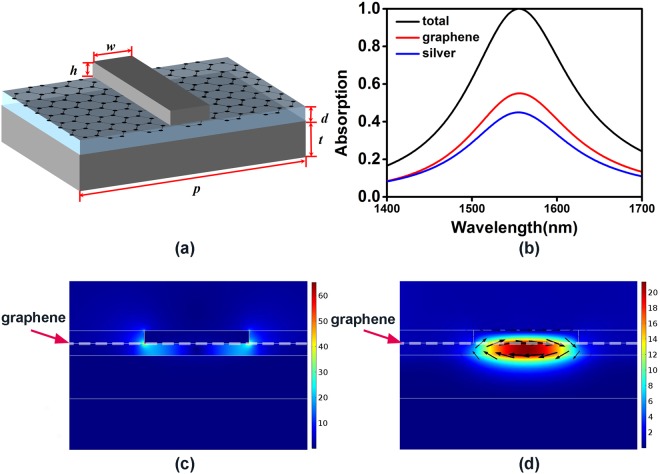
The schematic image of the unit cell of our proposed perfect absorption structure using magnetic dipole resonance is shown in Fig. 1(a). A monolayer graphene is sandwiched between a silver grating and a lossless alumina layer on top of a silver reflection mirror. The thickness of grating (h), dielectric layer (d) and reflection layer (t) are set as 30 nm, 28 nm and 100 nm, respectively. The width (w) and the period (p) of grating is 243 nm and 1000 nm.
Figure 1.
(a) Schematic of the unit cell of the graphene-based perfect absorption structure using magnetic dipole resonance. (b) Simulated total absorption spectrum and absorption spectra of the monolayer graphene and the metal. The electric and magnetic field distribution of the 1D metal grating structure at the resonant wavelength: (c) Normalized electric field at 1556 nm. (d) Normalized magnetic field at 1556 nm, where the black arrows represent electric displacement. The white dashed line marks the position of graphene in (c) and (d).
Figure 1(b) shows the absorption spectra of the designed structure for traverse-magnetic (TM) polarization. As shown in Fig. 1(b), the absorption peak of the structure is located at 1556 nm with total absorption over 99.9%, where the absorption of graphene and silver (including silver grating and silver mirror) are 55.1% and 44.9%, respectively. The full width at half maximum (FWHM) of total absorption is beyond 150 nm, one order higher than that of graphene-dielectric coupling structures15–18, and the over-50% absorption bandwidth of graphene is about 46 nm.
To analyze the physical mechanisms of the resonant mode related to the absorption peak in Fig. 1(b), we investigate the electromagnetic field and electric displacement distributions of the resonant mode in Fig. 1(c,d). The electromagnetic fields have been normalized with incident wave, and the direction and size of black arrows represent the direction and magnitude of electric displacement. It can be found that around 1556 nm, the electric field is mostly concentrated around bottom corners of the grating and the magnetic field is highly confined in the dielectric layer between the silver grating and silver reflection mirror. The electric displacement are focused around grating bottom and metal mirror top with opposite direction. These features are corresponded to characteristics of magnetic dipole resonance. Moreover, the electric and magnetic fields around graphene are enhanced over 60 and 20 times, respectively. Such strong localized electrical and magnetic fields efficiently enhance the absorption of graphene.
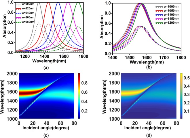
Figure 2(a,b) show the influence of geometric parameters of the structure on the absorption spectra of total structure (solid lines) and graphene (dashed lines). As shown in Fig. 2(a,b), absorption peak wavelength of the structure increases along with the increase of the grating width, but it is insensitive to the grating period since the magnetic dipole resonance is a kind of local surface plasmon polarizations. Simulation results show that the peak absorption of the total structure is nearly unchanged and the peak absorption of the graphene decreases slightly along with the increase of the grating width. And the effect of the grating period on the peak absorption of the structure can be nearly ignored in the grating period range from 1000 nm to 1200 nm. The angle-dependent feature of the structure toward TM polarization is presented in Fig. 2(c,d). The absorption spectra from 1400 nm to 1800 nm are stable with the incident angle less than 20 degree. A propagating surface plasmon mode interacts with the magnetic dipole resonance when the light illuminates at the angle from 20 degree to 40 degree, leading to an asymmetric line-shape in the absorption spectrum.
Figure 2.
The absorption spectra of total structure and graphene as functions of (a) grating width (b) structure period. Absorption of (c) total structure and (d) graphene as functions of the wavelength and incident angle for TM polarization. Other geometric parameters are fixed as in Fig. 1.
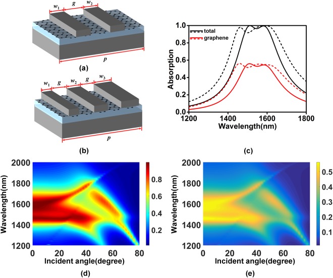
According to the conclusion that the wavelength of magnetic dipole resonance mainly depends on the grating width, we introduce two and three different width gratings in one period to broaden absorption bandwidth. The grating widths and air gap are set as w1 = 230 nm, w2 = 250 nm, g = 100 nm in Fig. 3(a), and w1 = 220 nm, w2 = 240 nm, w3 = 260 nm, g = 100 nm in Fig. 3(b). Other geometric parameters are the same as those in Fig. 1(a). Figure 3(c) shows the absorption spectra for the designed two-grating structure (solid lines) and three-grating structure (dashed lines). From Fig. 3(c), we could find that the over-50% absorption bandwidths of total structure and graphene are broadened to 240 nm and 128 nm for two-grating structure, 360 nm and 220 nm for three-grating structure.
Figure 3.
Schematic of the graphene-based absorption structures with (a) two and (b) three different gratings in one period. (c) The absorption spectra of total structure, graphene for the presented structures, where solid lines for (a) and dashed lines for (b), respectively. Absorption of (d) total structure and (f) graphene as functions of the wavelength and incident angle for the three-grating structure.
The angle-dependent absorption feature of multi-grating resonant structure is similar to that of single-grating resonant structure, as shown in Fig. 3(d–f). The peak absorption and absorption bandwidth are nearly unchanged in the incident angle range from 0 to 20 degree. When the incident angle is over 20 degree, a propagating mode occurs and destroys the stability of the absorption spectra versus incident angle.
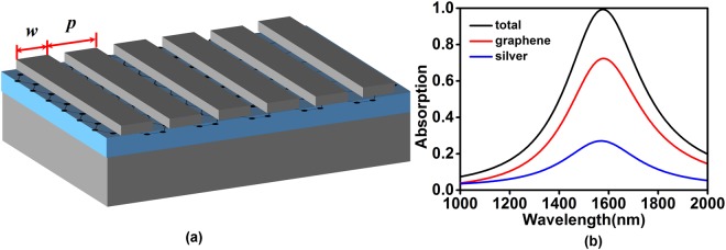
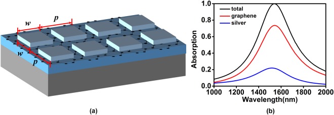
Next, we propose a deep sub-wavelength grating structure shown in Fig. 4(a) to enhance the absorption rate and bandwidth of graphene. The geometric parameters of the deep sub-wavelength structure are chosen as follows: p = 185 nm, w = 165 nm, h = 10 nm, d = 30 nm, t = 100 nm. Figure 4(b) shows the absorption spectra of the designed structure for TM polarization. As shown in Fig. 4(b), when the structure achieves the perfect absorption toward normally incident light with the wavelength of 1540 nm, the peak absorption of graphene approaches 75% with over-50% absorption bandwidth beyond 255 nm, and peak absorption of silver decreases from 45% to 25%, compared to the result in Fig. 1(b).
Figure 4.
(a) Schematic of the graphene-based deep sub-wavelength grating structure. (b) The absorption spectra of the total structure, graphene and metal in the (a).
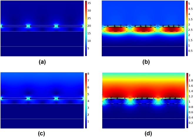
In order to reveal the physical origin of the absorption enhancement of graphene, the electromagnetic field distributions at on-resonant and off-resonant wavelengths are plotted in Fig. 5. Figure 5(a,b) show the electric field and magnetic field distributions of the structure at on-resonant wavelength of 1540 nm. As shown in Fig. 5(a), electric field mostly exists in the gaps between silver gratings, which lows the absorption of silver and improves that of graphene. In Fig. 5(b), the direction of electric displacement above and below lossless dielectric layer keeps opposite and almost unchanged along the boundaries of dielectric layer. From Fig. 5(a,b) we can see that the field distributions in the deep sub-wavelength structure at on-resonant wavelength are much different from that in the magnetic dipole resonance structure. This difference originates from the strong coupling of the fields in the adjacent grating units (i.e. magnetic coupling effect), since the gap between gratings in the deep sub-wavelength structure is as small as 20 nm. However, in Fig. 5(c,d), the electromagnetic field is not well confined around the graphene at off-resonant wavelength (1000 nm), resulting in the obvious reduction of graphene absorption.
Figure 5.
The electric and magnetic field distribution in the deep sub-wavelength structure at on-resonant wavelength (1540 nm) and off-resonant wavelength (1000 nm), where the black arrows represent electric displacement. (a) Normalized electric field at 1540 nm. (b) Normalized magnetic field at 1540 nm. (c) Normalized electric field at 1000 nm. (d) Normalized magnetic field at 1000 nm.
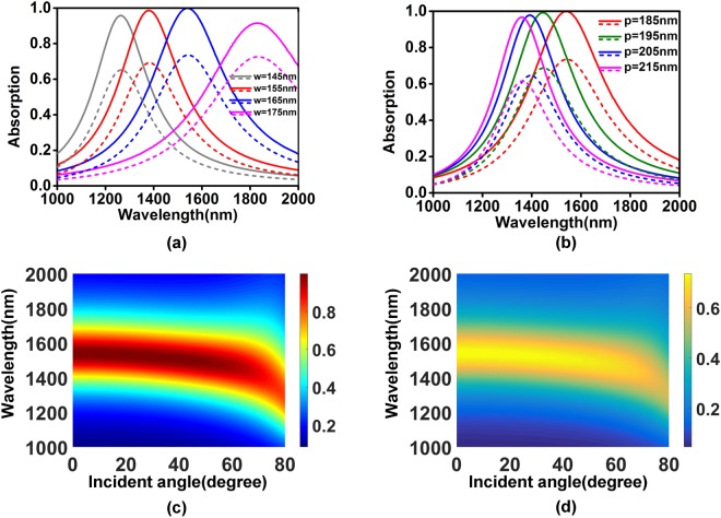
The influences of geometric parameters on the absorption of total structure and graphene are also calculated and shown in Fig. 6. Although the resonant wavelength of the structure is still dominated by the grating width, the period of the structure also becomes an important factor which affects the resonant wavelength. It can explained from Fig. 5(a,b) where the majority of electromagnetic field concentrates in the gap between gratings, thus the period plays a part in a similar way as the grating width does. In general, the rise of ratio of the grating width to the period causes a red shift on the absorption peak.
Figure 6.
The absorption spectra as functions of (a) grating width (b) structure period. Other parameters are fixed as in (a). Absorption spectra of (c) total structure and (d) graphene as functions as the wavelength and incident angle for TM polarization.
The absorption of the total structure and graphene as functions of wavelength and incident angle are shown in Fig. 6(c,d). When the angle varies from 0 to 40 degree, the absorption rate and absorption bandwidth of the structure are very stable, and the absorption peak wavelength only blue-shifts about 25 nm. The peak absorption wavelength and peak absorption rate reduce rapidly with the incident angle over 60 degree.
In order to overcome the polarization-dependent disadvantage in above structures, we propose a two-dimension (2D) monolayer-graphene-based structure with periodical square silver plates. The peripheral length of square plate is w = 165 nm, 20 nm less than the period of the structure, and other geometric parameters are same as those in Fig. 6(a). The graphene in the proposed structure shown in Fig. 7(a) could absorb 72% energy of the normally incident light with over-50%-absorption bandwidth about 240 nm.
Figure 7.
(a) Schematic of the graphene-based deep sub-wavelength 2D square plate structure. (b) The absorption spectra of the total structure, graphene and metal in the (a).
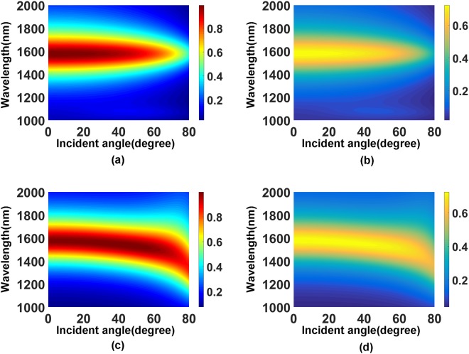
The influence of geometric parameters on the absorption for the 2D structure is similar to that plotted in the Fig. 6(a,b) for the 1D structure. The most important feature of the 2D structure is the polarization-independent absorption with the incident angle up to nearly 40 degree, as shown in Fig. 8.
Figure 8.
Absorption spectra as functions of the wavelength and incident angle for different polarization. (a) Total absorption for TE polarization. (b) Total absorption for TM polarization. (c) Graphene absorption for TE polarization. (d) Graphene absorption for TM polarization.
Conclusions
In summary, we proposed and analyzed two kinds of graphene-based perfect absorption structures in the near infrared. The absorption structure with multi-grating in a period by using magnetic dipole resonances could raise the peak absorption rate and over −50% absorption bandwidth of graphene up to 55% and 220 nm. And the absorption structure by utilizing magnetic coupling effects could improve the peak rate and absorption bandwidth to 74% and 255 nm. In addition, the demonstrated structures own ultrathin thickness and high graphene absorption, and can keep stable absorption rate and absorption bandwidth in a large incident angle range, which would be of valuable applications for graphene-based optoelectronic devices.
Methods
The proposed structures are analyzed using finite-element method-based software (Comsol Multiphysic). In the simulation, the monolayer graphene is regarded as a conductive surface with optical conductance of G0 ≈ 6.08 × 10⁻⁵ Ω−1, which corresponds to the absorption of 2.3% for a free standing graphene1,44,45. The refractive of alumina is taken as 1.646, and the dielectric constant of silver is given by Drude model as ε(ω) = ε∞ − ωp2/(ω2 + iγω) with ε∞ = 1.0, ωp = 1.37 × 10¹⁶ s−1, and γ = 6.66 × 10¹³ s−1. The damping constant (γ) of silver is doubled compared with the bulk value considering the surface scattering and grain boundary effects of the thin film.
Acknowledgements
The work is supported by National Natural Science Foundation of China (NSFC) (61404174 and 11674396), National University of Defense Technology Foundation (ZK17-03-17).
Author Contributions
C.G., Z.Z., W.X., F.W., X.Y. and S.Q. conceived the idea and supervised the study. Y.F. conducted the numerical simulations. Y.F. and C.G. wrote the manuscript. All authors contributed to the data analysis and reviewed the manuscript.
Competing Interests
The authors declare no competing interests.
Footnotes
Publisher's note: Springer Nature remains neutral with regard to jurisdictional claims in published maps and institutional affiliations.
References
- 1.Bonaccorso F, Sun Z, Hasan T, Ferrari AC. Graphene photonics and optoelectronics. Nat. Photonics. 2010;4:611–622. doi: 10.1038/nphoton.2010.186. [DOI] [Google Scholar]
- 2.Koppens FH, Chang DE, Garcia de Abajo FJ. Graphene plasmonics: a platform for strong light-matter interactions. Nano Lett. 2011;11:3370–3377. doi: 10.1021/nl201771h. [DOI] [PubMed] [Google Scholar]
- 3.Geim AK, Novoselov KS. The rise of graphene. Nat. materials. 2007;6:183–191. doi: 10.1038/nmat1849. [DOI] [PubMed] [Google Scholar]
- 4.Bao Q, Loh KP. Graphene photonics, plasmonics, and broadband optoelectronic devices. ACS nano. 2012;6:3677. doi: 10.1021/nn300989g. [DOI] [PubMed] [Google Scholar]
- 5.Bolotin KI, et al. Ultrahigh electron mobility in suspended graphene. Solid State Commun. 2008;146:351–355. doi: 10.1016/j.ssc.2008.02.024. [DOI] [Google Scholar]
- 6.Nair RR, et al. Fine structure constant defines visual transparency of graphene. Science. 2008;320:1308–1308. doi: 10.1126/science.1156965. [DOI] [PubMed] [Google Scholar]
- 7.Ju L, et al. Graphene plasmonics for tunable terahertz metamaterials. Nat. Nano. 2011;6:630–634. doi: 10.1038/nnano.2011.146. [DOI] [PubMed] [Google Scholar]
- 8.Zhan TR, Zhao FY, Hu XH, Liu XH, Zi J. Band structure of plasmons and optical absorption enhancement in graphene on subwavelength dielectric gratings at infrared frequencies. Phys. Rev. B Condensed Matter. 2012;86:125–132. [Google Scholar]
- 9.Thongrattanasiri S, Koppens FH, Garcia de Abajo FJ. Complete optical absorption in periodically patterned graphene. Phys. Rev. Lett. 2012;108:047401. doi: 10.1103/PhysRevLett.108.047401. [DOI] [PubMed] [Google Scholar]
- 10.Grigorenko AN, Polini M, Novoselov KS. Graphene plasmonics. Nat. Photonics. 2012;6:749–758. doi: 10.1038/nphoton.2012.262. [DOI] [Google Scholar]
- 11.Zhu ZH, et al. Electrically tunable polarizer based on anisotropic absorption of graphene ribbons. Appl. Phys. A. 2014;114:1017–1021. doi: 10.1007/s00339-014-8269-7. [DOI] [Google Scholar]
- 12.Gao F, et al. Broadband wave absorption in single-layered and nonstructured graphene based on far-field interaction effect. Opt. Express. 2017;25:9579. doi: 10.1364/OE.25.009579. [DOI] [PubMed] [Google Scholar]
- 13.Kim S, et al. Electronically Tunable Perfect Absorption in Graphene. Nano Lett. 2018;18:971–979. doi: 10.1021/acs.nanolett.7b04393. [DOI] [PubMed] [Google Scholar]
- 14.Furchi M, et al. Microcavity-integrated graphene photodetector. Nano Lett. 2011;12:2773. doi: 10.1021/nl204512x. [DOI] [PMC free article] [PubMed] [Google Scholar]
- 15.Gan X, et al. Strong enhancement of light-matter interaction in graphene coupled to a photonic crystal nanocavity. Nano Lett. 2012;12:5626. doi: 10.1021/nl302746n. [DOI] [PubMed] [Google Scholar]
- 16.Ferreira, A., Peres, N. M. R., Ribeiro, R. M. & Stauber, T. Efficient graphene-based photodetector with two cavities. Phys. Rev. B85 (2012).
- 17.Hashemi M, Farzad MH, Asger Mortensen N, Xiao S. Enhanced absorption of graphene in the visible region by use of plasmonic nanostructures. J. Opt. 2013;15:5003. doi: 10.1088/2040-8978/15/5/055003. [DOI] [Google Scholar]
- 18.Zhao B, Zhao JM, Zhang ZM. Enhancement of near-infrared absorption in graphene with metal gratings. Appl. Phys. Lett. 2014;105:666. [Google Scholar]
- 19.Xiong F, Zhang J, Zhu Z, Yuan X, Qin S. Ultrabroadband, More than One Order Absorption Enhancement in Graphene with Plasmonic Light Trapping. Sci. Rep. 2015;5:16998. doi: 10.1038/srep16998. [DOI] [PMC free article] [PubMed] [Google Scholar]
- 20.Ogawa S, Shimatani M, Fukushima S, Okuda S, Matsumoto K. Graphene on metal-insulator-metal-based plasmonic metamaterials at infrared wavelengths. Opt. Express. 2018;26:5665–5674. doi: 10.1364/OE.26.005665. [DOI] [PubMed] [Google Scholar]
- 21.Liu B, et al. Dual-band light absorption enhancement of monolayer graphene from surface plasmon polaritons and magnetic dipole resonances in metamaterials. Opt. Express. 2017;25:12061. doi: 10.1364/OE.25.012061. [DOI] [PubMed] [Google Scholar]
- 22.Liu B, et al. Tri-band absorption enhancement in monolayer graphene in visible spectrum due to multiple plasmon resonances in metal–insulator–metal nanostructure. Appl. Phys. Express. 2018;11:072201. doi: 10.7567/APEX.11.072201. [DOI] [Google Scholar]
- 23.Liu B, et al. Multiband and Broadband Absorption Enhancement of Monolayer Graphene at Optical Frequencies from Multiple Magnetic Dipole Resonances in Metamaterials. Nanoscale Res. Lett. 2018;13:153. doi: 10.1186/s11671-018-2569-3. [DOI] [PMC free article] [PubMed] [Google Scholar]
- 24.Liu B, et al. Electrically Tunable Fano Resonance from the Coupling between Interband Transition in Monolayer Graphene and Magnetic Dipole in Metamaterials. Sci. Rep. 2017;7:17117. doi: 10.1038/s41598-017-17394-y. [DOI] [PMC free article] [PubMed] [Google Scholar]
- 25.Piper JR, Fan S. Total Absorption in a Graphene Monolayer in the Optical Regime by Critical Coupling with a Photonic Crystal Guided Resonance. ACS Photonics. 2014;1:347–353. doi: 10.1021/ph400090p. [DOI] [Google Scholar]
- 26.Zou X, et al. Polarization-insensitive and wide-incident-angle optical absorber with periodically patterned graphene-dielectric arrays. Opt. Lett. 2018;43:46. doi: 10.1364/OL.43.000046. [DOI] [PubMed] [Google Scholar]
- 27.Liu Y, et al. Approaching total absorption at near infrared in a large area monolayer graphene by critical coupling. Appl. Phys. Lett. 2014;105:181105. doi: 10.1063/1.4901181. [DOI] [Google Scholar]
- 28.Grande M, et al. Graphene-based perfect optical absorbers harnessing guided mode resonances. Opt. Express. 2015;23:21032–21042. doi: 10.1364/OE.23.021032. [DOI] [PubMed] [Google Scholar]
- 29.Xu W, et al. Chip-integrated nearly perfect absorber at telecom wavelengths by graphene coupled with nanobeam cavity. Opt. Lett. 2015;40:3256–3259. doi: 10.1364/OL.40.003256. [DOI] [PubMed] [Google Scholar]
- 30.Guo CC, et al. Experimental Demonstration of Total Absorption over 99% in the Near Infrared for Monolayer-Graphene-Based Subwavelength Structures. Adv. Optical Mater. 2016;4:1955–1960. doi: 10.1002/adom.201600481. [DOI] [Google Scholar]
- 31.Fan YS, et al. Monolayer-graphene-based perfect absorption structures in the near infrared. Opt. Express. 2017;25:13079. doi: 10.1364/OE.25.013079. [DOI] [PubMed] [Google Scholar]
- 32.Jiang X, Wang T, Xiao S, Yan X, Cheng L. Tunable ultra-high-efficiency light absorption of monolayer graphene using critical coupling with guided resonance. Opt. Express. 2017;25:27028. doi: 10.1364/OE.25.027028. [DOI] [PubMed] [Google Scholar]
- 33.Lee S, Tran TQ, Heo H, Kim M, Kim S. A proposal of a perfect graphene absorber with enhanced design and fabrication tolerance. Sci. Rep. 2017;7:4760. doi: 10.1038/s41598-017-04995-w. [DOI] [PMC free article] [PubMed] [Google Scholar]
- 34.Zhang, H., Zheng, G., Xian, F., Zou, X. & Wang, J. Near-unity absorption of graphene monolayer with a triple-layer waveguide coupled grating. Opt. Materials 72 (2017).
- 35.Guo J, Wu L, Dai X, Xiang Y, Fan D. Absorption enhancement and total absorption in a graphene-waveguide hybrid structure. Aip Adv. 2017;7:025101. doi: 10.1063/1.4975706. [DOI] [Google Scholar]
- 36.Koechlin C, et al. Total routing and absorption of photons in dual color plasmonic antennas. Appl. Phys. Lett. 2011;99:241104. doi: 10.1063/1.3670051. [DOI] [Google Scholar]
- 37.Cui Y, et al. A thin film broadband absorber based on multi-sized nanoantennas. Appl. Phys. Lett. 2011;99:253101. doi: 10.1063/1.3672002. [DOI] [Google Scholar]
- 38.Cheng CW, et al. Wide-angle polarization independent infrared broadband absorbers based on metallic multi-sized disk arrays. Opt. Express. 2012;20:10376–10381. doi: 10.1364/OE.20.010376. [DOI] [PubMed] [Google Scholar]
- 39.Bouchon P, Koechlin C, Pardo F, Haïdar R, Pelouard JL. Wideband omnidirectional infrared absorber with a patchwork of plasmonic nanoantennas. Opt. Lett. 2012;37:1038. doi: 10.1364/OL.37.001038. [DOI] [PubMed] [Google Scholar]
- 40.Chettiar UK, Kildishev AV, Klar TA, Shalaev VM. Negative index metamaterial combining magnetic resonators with metal films. Opt. Express. 2006;14:7872–7877. doi: 10.1364/OE.14.007872. [DOI] [PubMed] [Google Scholar]
- 41.Kildishev AV, et al. A negative permeability material at red light. Opt. Express. 2007;15:1076–1083. doi: 10.1364/OE.15.001076. [DOI] [PubMed] [Google Scholar]
- 42.Hao J, et al. High performance optical absorber based on a plasmonic metamaterial. Appl. Phys. Lett. 2010;96:4184. [Google Scholar]
- 43.Guo C, et al. Magnetic coupling metasurface for achieving broad-band and broad-angular absorption in the MoS2 monolayer. Opt. Mater. Express. 2017;7:100. doi: 10.1364/OME.7.000100. [DOI] [Google Scholar]
- 44.Kuzmenko AB, van Heumen E, Carbone F, van der Marel D. Universal optical conductance of graphite. Phys. Rev. Lett. 2008;100:117401. doi: 10.1103/PhysRevLett.100.117401. [DOI] [PubMed] [Google Scholar]
- 45.Stauber T, Peres NMR, Geim AK. Optical conductivity of graphene in the visible region of the spectrum. Phys. Rev. B. 2008;78:8. [Google Scholar]
- 46.Groner MD, Fabreguette FH, Elam JW, George SM. Low-Temperature Al2O3 Atomic Layer Deposition. Chem. Mater. 2004;16:639–645. doi: 10.1021/cm0304546. [DOI] [Google Scholar]


