Summary
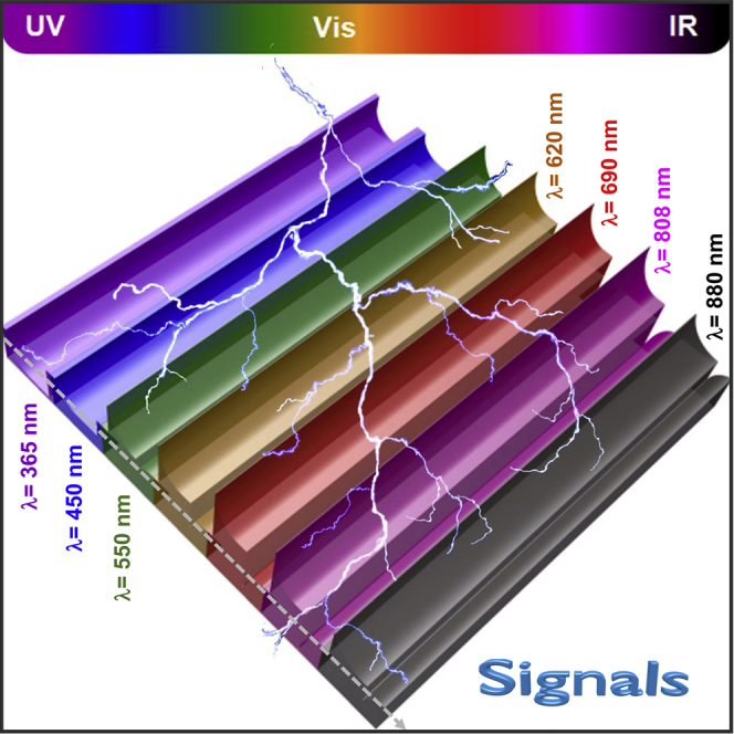
Self-powered photodetectors are expected to play a crucial role in future nano-optoelectronic devices owing to their independent and sustainable operation. Based on the heterojunction between ZnO nanowires (NWs) and shuttle-like SnS, we design a self-powered photodetector exhibiting wide-range photoresponse and tunable spectral selectivity. Differently from conventional devices, a wavelength-induced photocurrent polarity is observed in the ZnO NWs/SnS photodetector, which enables the device to distinguish between photons in the UV and visible (VIS) regions. This is due to switching of the interfacial modulation by the pyroelectric-polarization potential (pyro-potential) inside ZnO NWs and thermoelectric-polarization potential (thermo-potential) inside SnS. A photocurrent enhancement of 125% and improved responsivity of 364 μA/W are obtained under the pyro-potential upon 690 nm light illumination, whereas reversed responsivity of −155 μA/W is obtained under the thermo-potential upon 365 nm light illumination. We believe the photocurrent polarity could be useful for improving resolution of dynamic light sensing/imaging.
Subject Areas: Optoelectronics, Nanotechnology Fabrication, Energy Materials
Graphical Abstract
Highlights
-
•
A unique signal polarity is observed in self-powered ZnO/SnS photodetector
-
•
It enables recognition of photons in the ultraviolet region and visible region
-
•
The principle relies on the pyro-potential in ZnO and thermo-potential in SnS
Optoelectronics; Nanotechnology Fabrication; Energy Materials
Introduction
Self-powered photodetectors have received considerable attention owing to their improved adaptability and mobility in long-term detecting, communicating, responding, and imaging applications (Yang et al., 2010, Konstantatos and Sargent, 2010, Ma et al., 2017, Konstantatos et al., 2006, Wang and Kim, 2017, Ni et al., 2013). Normally, the design of self-powered photodetectors is based on either an integrated energy harvesting unit or an internal built-in electric field, which is necessary for separating the photo-generated charge pairs (electrons and holes) and thus forming photocurrent (Peng et al., 2014, Su et al., 2017, Wang et al., 2015, Choi et al., 2009, Ouyang et al., 2017, Chen et al., 2016). During the optoelectronic process, the direction of the photo-generated electric field is opposite to that of the built-in electric field, which can weaken the separation of charge carriers (Wang et al., 2017, Heeger, 2014). Up to now, the p-n junction and Schottky barrier have been widely utilized to enhance built-in electric fields (Zhao et al., 2017, Wu et al., 2016, Peng et al., 2017, Yu et al., 2017, Zhang et al., 2012, Xiang et al., 2015, Wu and Wang, 2016). However, the built-in potentials in these studies are always insufficient to control the transfer direction of charge pairs, limiting the resolution of dynamic light imaging and detection. Therefore, it is necessary and essential to select apposite optical/electrical materials and promote the configuration design of self-powered photodetectors to realize optimal optoelectronic process.
As is well known, ZnO in wurtzite lattice is a direct band-gap nonferroelectrics lacking a center of symmetry with high total pyroelectric coefficient (−9.4 μC⋅m−2⋅K−1) (Heiland and Ibach, 1966, Lang, 2005, Norton et al., 2004); SnS is an indirect band-gap semiconductor with predicted high Seebeck coefficient (400 μV⋅K−1) and low thermal conductivity (17 mW⋅cm−1⋅K−1) (Tan et al., 2014, Spitzer, 1970, Xu et al., 2009). Rapid change of temperature can be naturally induced by light illuminations, leading to independent built-in potentials within the above-mentioned anisotropic semiconductors. Our thought is to combine the pyroelectric characteristic of ZnO nanowire (NW) and thermoelectric characteristic of SnS together to modulate the optoelectronic process and thus realize polarity control of the charge transfer by utilizing the heat effect of light illumination.
In the design, there are two opposite built-in electric fields in self-powered ZnO NWs/SnS photodetector: the pyroelectric-polarization potential (pyro-potential) inside ZnO, which promotes the optoelectronic process, and the thermo-potential inside SnS, which suppresses the optoelectronic process. As expected, a photocurrent enhancement of 125% and improved responsivity of 364 μA/W are obtained under visible (VIS) illumination (690 nm), whereas a reverse responsivity of −155 μA/W is obtained under UV illumination (365 nm) for the special ZnO NWs/SnS photodetector at zero bias. Furthermore, a 6 × 6 photodetector array with 36 pixels is constructed to indicate the good resolution of switchable light imaging. In comparison with conventional photodetectors, the unique light wavelength-induced photocurrent polarity in the self-powered ZnO NWs/SnS photodetector shows prospect in the fields of wide-range light imaging, binary switches, as well as optoelectronic integrated circuits.
Results
Device Structure and Characterization
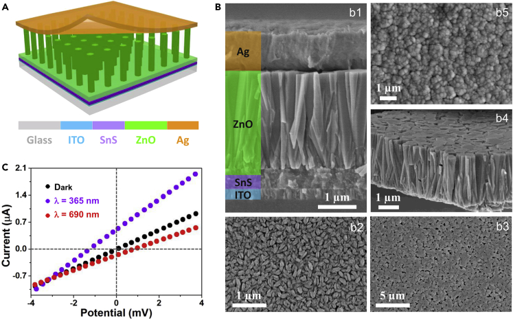
Figure 1A illustrates the schematic structure of the self-powered ZnO NWs/SnS photodetector, which consists of a transparent glass substrate, the bottom electrode of indium tin oxide (ITO) film, a layer of p-SnS film, a layer of ZnO NW array, and the top electrode of silver (Ag) film. Detailed fabrication processes of the devices are given in Supplemental Information (see Transparent Methods). The cross-sectional scanning electron microscopy (SEM) image confirms the configuration of the final device, which possesses an effective thickness of approximately 4 μm (b1 of Figure 1B). The top-view SEM image of the as-deposited SnS film by radio frequency (RF) magnetron sputtering indicates that the ITO glass substrate is compactly covered by shuttle-like SnS nanostructures (b2 of Figure 1B). The densely packed crystallites and large textured grains suggest excellent light absorption performance of the shuttle-like SnS (Banai et al., 2013). Hexagonal prism-shaped ZnO NWs with diameters of about 500 nm are highly oriented and densely grown on the SnS film (b3 of Figure 1B). The average length of the as-grown ZnO NW array is estimated to be ∼2 μm (b4 of Figure 1B). From the top-view SEM image of the device, it can be seen that a compact Ag film composed of dense nanoparticles is formed on the device surface (b5 of Figure 1B), suggesting good conductivity of the top electrode. The current-voltage (I-V) characteristics of a representative device (1.5 × 1.5 mm2) were measured under dark, 365 nm light illumination, and 690 nm light illumination, indicating good rectifying characteristic of the ZnO NWs/SnS heterojunction photodetector (Figure S1A). As shown in the enlarged I-V curves, the device demonstrates good UV response with positive photocurrent of 535 nA under 365 nm light illumination (purple curve in Figure 1C), whereas a negative photocurrent of −144 nA is obtained under 690 nm light illumination (red curve in Figure 1C), indicating switchable behavior of the self-powered ZnO NWs/SnS heterojunction photodetector.
Figure 1.
Structure and Characterization of Self-Powered ZnO NWs/SnS Photodetector
(A) Schematic diagram showing the structure of the photodetector.
(B) SEM image of the ZnO NWs/SnS photodetector: (b1) cross-sectional view of a fabricated device, (b2) top view of the as-deposited shuttle-like SnS nanostructures, (b3) top view of the as-grown ZnO NWs, (b4) tilted cross-sectional view of the ZnO NWs, and (b5) top view of the as-deposited Ag electrode.
(C) I-V characteristics of the device measured under dark, 365 nm light illumination (93.5 mW/cm2), and 690 nm light illumination (23.3 mW/cm2).
See also Figure S1.
General Performance
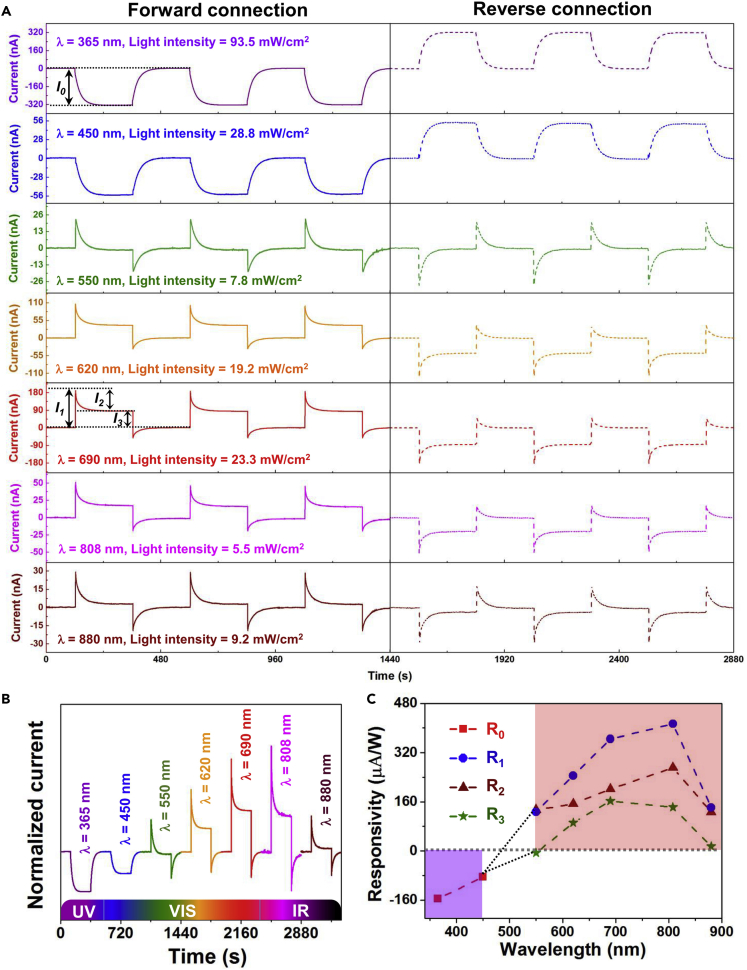
The photoresponse of self-powered ZnO NWs/SnS photodetector was investigated systematically under light illuminations with different wavelengths ranging from 365 to 880 nm. As depicted in Figures 2A and S2, reversed output signals are observed at zero bias under forward and reverse connections, suggesting that the measured signals were generated by the fabricated device. Under forward connection, negative current signals of −326 and −54 nA are observed under 365 nm light illumination (93.5 mW/cm2) and 450 nm light illumination (28.8 mW/cm2), respectively. After light illumination with larger wavelengths, the obtained signals are switched in sign, possessing obvious two-stage photoresponse characteristics. The measured short-circuit current sharply increases to a peak value of I1 and then moves toward stabilization until a platform of I3 owing to the photovoltaic performance of the ZnO NWs/SnS heterojunction. The tip current of I2 = I1 − I3 can be attributed to the pyroelectric effect inside the ZnO NW array due to the heat effect of light illumination (Zhang et al., 2016). For example, positive current signals of I1 ≈ 191 nA, I2 ≈ 106 nA, and I3 ≈ 85 nA are observed under 690 nm light illumination (23.3 mW/cm2). It is worth noting that a photocurrent enhancement of ∼125% is produced by the illumination-induced pyroelectric effect of ZnO NWs. The output currents and voltages of the self-powered ZnO NWs/SnS photodetector under two representative types of illuminations, UV light illumination (λ = 365 nm) as well as VIS light illumination (λ = 690 nm), were further investigated under various light intensities. As presented in Figures S3 and S4, the magnitude of photocurrent and photovoltage increases linearly with the light intensity for both UV and VIS light illuminations. Therefore, the obtained photocurrent curves in Figure 2A were normalized by light intensity and plotted in Figure 2B for a clearer comparison. It can be seen that negative current signals are observed upon light illuminations with wavelengths shorter than 450 nm, whereas positive current signals are observed upon light illuminations with wavelengths longer than 550 nm. Specially noted, the switchable behavior around wavelength of 500 nm suggests a different mechanism of photoresponse, implying a light wavelength-induced photocurrent polarity controlling strategy for the self-powered photodetector system, which will be discussed thoroughly later.
Figure 2.
General Performance of Self-Powered ZnO NWs/SnS Photodetector
(A) Measured short-circuit currents of the device at forward connection and reverse connection, when it was subjected to different light illuminations.
(B) Normalized photocurrent of the device under light illuminations with different wavelengths.
(C) Wavelength-dependent responsivities of the device, revealing wavelength-induced signal polarity.
See also Figures S2–S6.
To better understand the controlling strategy, the wavelength-dependent responsivity of the self-powered ZnO NWs/SnS photodetector is demonstrated in Figure 2C. The responsivity (R1, R2, and R3) under each light illumination was calculated based on R = (Ilight − Idark)/(P⋅A) (Koppens et al., 2014), where Ilight, Idark, P, and A are the photocurrent, dark current, incident light intensity, and effective area, respectively. The responsivity increases with light wavelengths ranging from 365 to 808 nm. Upon 880 nm light illumination, the output signal and the corresponding responsivity decrease, because the light (λ > 800 nm) is hardly absorbed by ZnO or SnS. The calculated responsivity of the ZnO NWs/SnS photodetector is R1 = R3 = −155 μA/W for 365 nm light illumination, whereas the responsivity is R1 = 364 μA/W and R3 = 163 μA/W for 690 nm light illumination. In addition, series-resistance-dependent I-t characteristics of the self-powered photodetector depict that the device possesses a maximum output power of P1/P2 = 105.6 pW for 365 nm light illumination at 4 KΩ and P1/P2/P3 = 54.2 pW/15.1 pW/12.1 pW for 690 nm light illumination at 8 KΩ (Figure S5). For dynamic imaging, it is also important to evaluate the frequency response of the photodetector (Mueller et al., 2010). By modulating the incident light with a mechanical chopper, the photocurrents under different chopping frequencies were measured. As shown in Figure S6, the response speed of the photodetector under VIS light illumination (λ = 690 nm) is much faster than that under UV light illumination (λ = 365 nm). The dynamic current signals along with operation frequency might have potential applications in low-speed (<10 Hz) motion detection and dynamic light imaging. These characteristics make the proposed ZnO NWs/SnS photodetector superior to other semiconductor photodetectors, especially in distinguishing photons with wavelengths in the UV region and VIS region.
Operation Mechanism
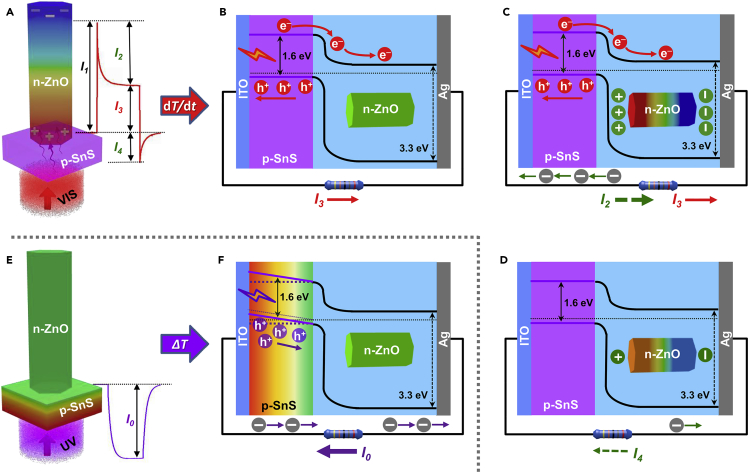
As demonstrated in Figure 3A, the signal of VIS light illumination displays a sharp rising edge and a plateau (I1 = I2 + I3), corresponding to two optical processes in the device: the photoexcitation at the local junction caused by the photoabsorption and the instantaneous pyro-potential inside ZnO NWs (Figures 3B–3D). Normally, the light illumination produces free carriers as photocurrent to transport through the external circuit from the ITO electrode to Ag electrode owing to type II band alignment (Zhu et al., 2017, Li et al., 2015) of the ZnO NWs/SnS heterojunction (Figure 3B). On the basis of the transmittance spectra depicted in Figure S1B, the deposited SnS layer is partially transparent to VIS light illumination (λ = 690 nm) but absolutely opaque to UV light illumination (λ = 365 nm). Under the heat effect of VIS light illumination, the temperature inside ZnO NWs increases (ΔT > 0, dT/dt > 0), resulting in a distribution of polarization charges along the c-axis of ZnO NWs with localized positive charges at the heterojunction interface and negative charges at the Ag electrode side. To balance the pyroelectric polarization potential, the induced charges on the electrodes would be redistributed along with the increase of temperature, resulting in electron flow in the external circuit from the Ag electrode to the ITO electrode (Figure 3C). Here, the sharp peak (I1) in the I-t curve (Figure 3A) can be seen as the combination of the pyroelectric current (I2) and the photovoltaic current (I3). When the light illumination is retained and the temperature reaches a higher and stable value, the output current reaches a plateau, which is recognized as the net photovoltaic current of I3. When the light illumination is turned off, the photovoltaic current rapidly disappears and the increased temperature gradually recovers to initial room temperature (ΔT < 0, dT/dt < 0), resulting in a negative pyroelectric current (I4) due to the reverse pyroelectric potential, as shown in Figure 3D. Herein, the heat-enhanced photocurrent by VIS light illumination reflects a coupling effect of pyroelectricity, photoexcitation, and semiconductor characteristics on interfacial charge transfer, which is called pyro-phototronics (as clarified in Figure S7A).
Figure 3.
Operation Mechanism of Self-Powered ZnO NWs/SnS Photodetector
(A) Schematic diagram of the pyro-potential inside ZnO NW and a typical cycle of I-t curve under VIS illumination (λ = 690 nm).
(B) Energy-band diagram and the photoexcitation at the local ZnO/SnS heterojunction.
(C) Energy-band diagram of the device upon VIS illumination, indicating pyro-phototronic effect on the device performance.
(D) Energy-band diagram of the device when turning off the VIS light illumination, leading to decreased temperature inside ZnO NWs and reverse pyroelectric current.
(E) Schematic diagram of the thermo-potential inside SnS film and a typical cycle of I-t curve under UV illumination (λ = 365 nm).
(F) Energy-band diagram of the device upon UV illumination, indicating thermo-phototronic effect on the device performance.
See also Figures S1 and S7–S10.
For UV light illumination, the light is fully absorbed by the SnS layer, leading to a temperature gradient inside SnS. No UV light can reach the ZnO NWs. The negative current signal (I0) thus can be explained by the complex effect of photoexcitation caused by photoabsorption and thermo-potential inside SnS (Figures 3B, 3E, and 3F). As depicted in Figure 3F, an inner thermo-potential (VTE) will be induced across SnS under the heat effect of UV illumination due to the difference between the Fermi levels of the two ends of SnS. Driven by the VTE, the photovoltaic current generated by the transport of holes in the p-SnS toward the ITO electrode is suppressed, finally resulting in electron flow in the external circuit from the ITO electrode to the Ag electrode. Additional measurements were conducted to further explore and confirm the origin of the thermoelectric current across SnS. An ITO/SnS/Ag ohmic-junction device without a ZnO layer was fabricated and studied, which can generate a negative current of approximately −50 μA under the same UV light illumination (Figure S8). The current signal of the ITO/SnS/Ag ohmic-junction device (μA-level) is larger than that of the ITO/SnS/ZnO/Ag heterojunction device (nA-level), which can be ascribed to the shielded photovoltaic effect in the ohmic-junction device. Afterward, the Ag electrode in the ITO/SnS/Ag device was further replaced by the ITO electrode to be able to alter the direction of light illumination. Reversed output current/voltage signals are observed with upward illumination and downward illumination (reversed temperature gradient inside SnS induced by light illumination), suggesting that the measured signals are truly generated by the thermoelectric characteristic of SnS (Figures S9 and S10). Herein, the ΔT-induced photocurrent of the ZnO NWs/SnS heterojunction by UV light illumination reflects the coupling effect of thermoelectricity, photoexcitation, and semiconductor characteristics, called as the thermo-phototronics (Figure S7B). These results consistently confirm the light wavelength-induced photocurrent polarity in the self-powered ZnO NWs/SnS photodetector.
Application as Switchable Light Imaging
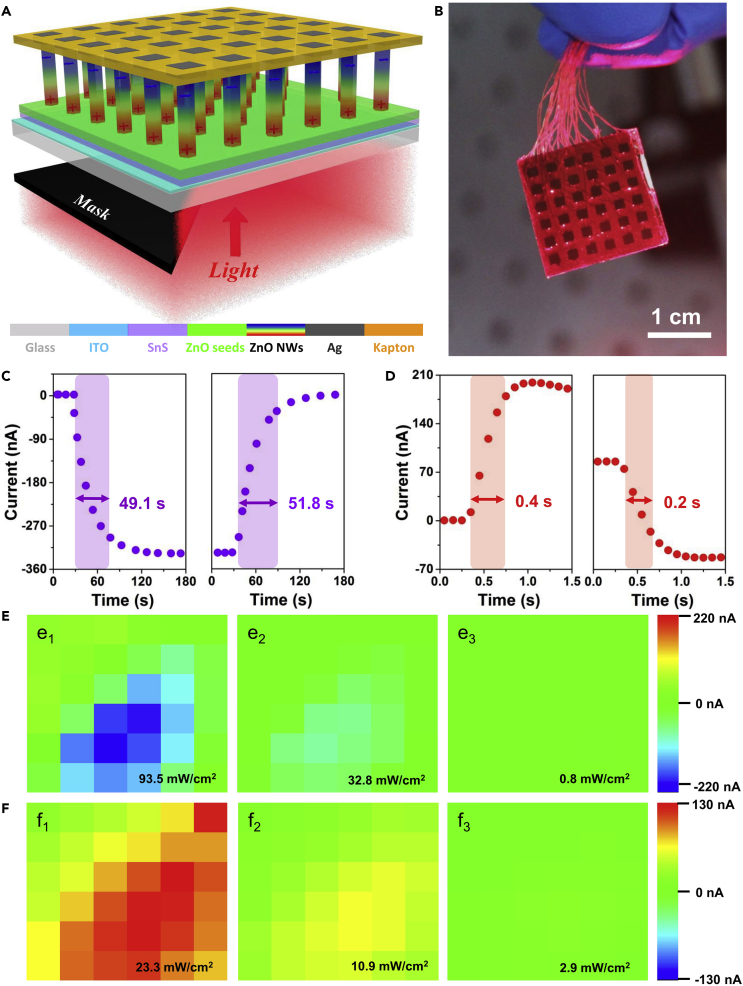
To demonstrate the potential application of the ZnO NWs/SnS heterojunction, we fabricated a multi-channel (6 × 6) photodetector array with 36 pixels in the total area of 2 cm × 2 cm, as shown in Figures 4A and 4B. The active area of each pixel is approximately 1.5 × 1.5 mm2. From the viewpoint of light imaging performance, the response/recovery time of the self-powered ZnO NWs/SnS photodetector was found to be ∼49.1 s/51.8 s for 365 nm UV light illumination (Figure 4C) and ∼0.4 s/0.2 s for 690 nm VIS light illumination (Figure 4D). A series of imaging tests were then performed with the top-left part of the photodetector masked, keeping the lower right part under light illumination (Figures S11 and S12). Upon light illumination, the complete imaging figure can clearly distinguish the illuminated pixel from the surrounding pixels by monitoring the current signal of each independent pixel. As shown in Figures 4E and 4F, imaging figures with blue pixels (negative current signals) are observed under UV light illumination, whereas imaging figures with red pixels (positive current signals) are observed under VIS light illumination, indicating good resolution and switchable light imaging behavior of the self-powered ZnO NWs/SnS photodetector array.
Figure 4.
Schematic and Performance of Self-Powered ZnO NWs/SnS Photodetector System
(A) Schematic of a 36-channel photodetector system with the lower right part under light illumination.
(B) Photograph of an as-fabricated 6 × 6 photodetector array with each pixel being 1.5 mm × 1.5 mm.
(C and D) Response and recovery time of the photodetector system under (C) 365 nm light illumination and (D) 690 nm light illumination.
(E and F) Photocurrent imaging figure under (E) 365 nm light illumination and (F) 690 nm light illumination with different light intensities.
See also Figures S11 and S12.
Discussion
The self-powered ZnO NWs/SnS heterojunction photodetector possesses a unique light wavelength-induced photocurrent polarity in comparison with conventional photosensing devices. On the one hand, the pyro-potential inside ZnO toward visible light illuminations was employed to enhance the photosensing performance. A photocurrent enhancement of ∼125% is produced by the illumination-induced pyroelectric effect of ZnO NWs. On the other hand, the ZnO NWs/SnS photodetector demonstrates suppressed charge transfer by thermo-potential inside SnS toward UV light illuminations. Switched photocurrent polarity implies switchable light imaging strategy for self-powered photodetector. The pyroelectric effect and thermoelectric effect alternatively act on the photovoltaic effect of the ZnO NWs/SnS heterojunction in one device, leading to a wide-range photoresponse and tunable spectral selectivity. For both UV and VIS light illuminations, the magnitude of the photocurrent and photovoltage increases linearly with the light intensity. Maximized responsivity of −155 μA/W is obtained under 365 nm UV light illumination, and maximized responsivity of 364 μA/W is obtained under 690 nm VIS light illumination. Finally, we fabricated a multi-channel (6 × 6) photodetector array with 36 pixels, indicating good resolution and switchable light imaging behavior of the self-powered ZnO NWs/SnS photodetector array. We believe that the light wavelength-induced photocurrent polarity could be useful for improving the resolution of dynamic light sensing/imaging.
Methods
All methods can be found in the accompanying Transparent Methods supplemental file.
Acknowledgments
This work was supported by the National Key R&D Program of China (Grant No. 2016YFA0202701), the National Natural Science Foundation of China (Grant Nos. 61604012, 51472055, 61404034), External Cooperation Program of BIC, Chinese Academy of Sciences (Grant No. 121411KYS820150028), the 2015 Annual Beijing Talents Fund (Grant No. 2015000021223ZK32), and the "thousands talents" program for the pioneer researcher and his innovation team, China.
Author Contributions
Conceptualization, Y.Y.; Experiments, B.O. and K.Z.; Discussions, B.O., K.Z., and Y.Y.; Writing, B.O., K.Z., and Y.Y; Funding Acquisition, K.Z. and Y.Y.; Supervision, Y.Y.
Declaration of Interests
The authors declare no competing interests.
Published: March 23, 2018; corrected online: April 4, 2018
Footnotes
Supplemental Information includes Transparent Methods and 12 figures and can be found with this article online at https://doi.org/10.1016/j.isci.2018.01.002.
Supplemental Information
References
- Banai R.E., Lee H., Motyka M.A., Chandrasekharan R., Podraza N.J., Brownson J.R., Horn M.W. Optical properties of sputtered SnS thin films for photovoltaic absorbers. IEEE J. Photovolt. 2013;3:1084–1089. [Google Scholar]
- Chen H., Liu H., Zhang Z., Hu K., Fang X. Nanostructured photodetectors: from ultraviolet to terahertz. Adv. Mater. 2016;28:403–433. doi: 10.1002/adma.201503534. [DOI] [PubMed] [Google Scholar]
- Choi T., Lee S., Choi Y.J., Kiryukhin V., Cheong S.W. Switchable ferroelectric diode and photovoltaic effect in BiFeO3. Science. 2009;324:63–66. doi: 10.1126/science.1168636. [DOI] [PubMed] [Google Scholar]
- Heeger A.J. 25th anniversary article: bulk heterojunction solar cells: understanding the mechanism of operation. Adv. Mater. 2014;26:10–27. doi: 10.1002/adma.201304373. [DOI] [PubMed] [Google Scholar]
- Heiland G., Ibach H. Pyroelectricity of zinc oxide. Solid State Commun. 1966;4:353–354. [Google Scholar]
- Konstantatos G., Sargent E.H. Nanostructured materials for photon detection. Nat. Nanotech. 2010;5:391–400. doi: 10.1038/nnano.2010.78. [DOI] [PubMed] [Google Scholar]
- Konstantatos G., Howard I., Fischer A., Hoogland S., Clifford J., Klem E., Levina L., Sargent E.H. Ultrasensitive solution-cast quantum dot photodetectors. Nature. 2006;442:180–183. doi: 10.1038/nature04855. [DOI] [PubMed] [Google Scholar]
- Koppens F.H.L., Mueller T., Avouris P., Ferrari A.C., Vitiello M.S., Polini M. Photodetectors based on graphene, other two-dimensional materials and hybrid systems. Nat. Nanotech. 2014;9:780–793. doi: 10.1038/nnano.2014.215. [DOI] [PubMed] [Google Scholar]
- Lang S.B. Pyroelectricity: from ancient curiosity to modern imaging tool. Phys. Today. 2005;58:31–36. [Google Scholar]
- Li H., Zhou Y., Tu W., Ye J., Zou Z. State-of-the-art progress in diverse heterostructured photocatalysts toward promoting photocatalytic performance. Adv. Funct. Mater. 2015;25:998–1013. [Google Scholar]
- Ma N., Zhang K., Yang Y. Photovoltaic-pyroelectric coupled effect induced electricity for self-powered photodetector system. Adv. Mater. 2017;29:1703694. doi: 10.1002/adma.201703694. [DOI] [PubMed] [Google Scholar]
- Mueller T., Xia F., Avouris P. Graphene photodetectors for high-speed optical communications. Nat. Photon. 2010;4:297–301. [Google Scholar]
- Ni P.N., Shan C.X., Wang S.P., Liu X.Y., Shen D.Z. Self-powered spectrum-selective photodetectors fabricated from n-ZnO/p-NiO core-shell nanowire arrays. J. Mater. Chem. C. 2013;1:4445–4449. [Google Scholar]
- Norton D.P., Heo Y.W., Ivill M.P., Ip K., Pearton S.J., Chisholm M.F., Steiner T. ZnO: growth, doping & processing. Mater. Today. 2004;7:34–40. [Google Scholar]
- Ouyang B., Zhang K., Yang Y. Self-powered UV photodetector array based on P3HT/ZnO nanowire array heterojunction. Adv. Mater. Technol. 2017;2:1700208. [Google Scholar]
- Peng L., Hu L., Fang X. Energy harvesting for nanostructured self-powered photodetectors. Adv. Funct. Mater. 2014;24:2591–2610. [Google Scholar]
- Peng W., Wang X., Yu R., Dai Y., Zou H., Wang A.C., He Y., Wang Z.L. Enhanced performance of a self-powered organic/inorganic photodetector by pyro-phototronic and piezo-phototronic effects. Adv. Mater. 2017;29:1606698. doi: 10.1002/adma.201606698. [DOI] [PubMed] [Google Scholar]
- Spitzer D.P. Lattice thermal conductivity of semiconductors: a chemical bond approach. J. Phys. Chem. Solids. 1970;31:19–40. [Google Scholar]
- Su L., Yang W., Cai J., Chen H., Fang X. Self-powered ultraviolet photodetectors driven by built-in electric field. Small. 2017;13:1701687. doi: 10.1002/smll.201701687. [DOI] [PubMed] [Google Scholar]
- Tan Q., Zhao L.D., Li J.F., Wu C.F., Wei T.R., Xing Z.B., Kanatzidis M.G. Thermoelectrics with earth abundant elements: low thermal conductivity and high thermopower in doped SnS. J. Mater. Chem. A. 2014;2:17302–17306. [Google Scholar]
- Wang H., Kim D.H. Perovskite-based photodetectors: materials and devices. Chem. Soc. Rev. 2017;46:5204–5236. doi: 10.1039/c6cs00896h. [DOI] [PubMed] [Google Scholar]
- Wang X., Wang P., Wang J., Hu W., Zhou X., Guo N., Huang H., Sun S., Shen H., Lin T. Ultrasensitive and broadband MoS2 photodetector driven by ferroelectrics. Adv. Mater. 2015;27:6575–6581. doi: 10.1002/adma.201503340. [DOI] [PubMed] [Google Scholar]
- Wang X., Dai Y., Liu R., He X., Li S., Wang Z.L. Light-triggered pyroelectric nanogenerator based on a pn-junction for self-powered near-infrared photosensing. ACS Nano. 2017;11:8339–8345. doi: 10.1021/acsnano.7b03560. [DOI] [PubMed] [Google Scholar]
- Wu W., Wang Z.L. Piezotronics and piezo-phototronics for adaptive electronics and optoelectronics. Nat. Rev. Mater. 2016;1:16031. [Google Scholar]
- Wu C.Y., Pan Z.Q., Wang Y.Y., Ge C.W., Yu Y.Q., Xu J.Y., Wang L., Luo L.B. Core-shell silicon nanowire array-Cu nanofilm Schottky junction for a sensitive self-powered near-infrared photodetector. J. Mater. Chem. C. 2016;4:10804–10811. [Google Scholar]
- Xiang D., Han C., Hu Z., Lei B., Liu Y., Wang L., Hu W.P., Chen W. Surface transfer doping-induced, high-performance graphene/silicon Schottky junction-based, self-powered photodetector. Small. 2015;11:4829–4836. doi: 10.1002/smll.201501298. [DOI] [PubMed] [Google Scholar]
- Xu Y., Al-Salim N., Bumby C.W., Tilley R.D. Synthesis of SnS quantum dots. J. Am. Chem. Soc. 2009;131:15990–15991. doi: 10.1021/ja906804f. [DOI] [PubMed] [Google Scholar]
- Yang Y., Guo W., Qi J., Zhao J., Zhang Y. Self-powered ultraviolet photodetector based on a single Sb-doped ZnO nanobelt. Appl. Phys. Lett. 2010;97:223113. [Google Scholar]
- Yu X.X., Yin H., Li H.X., Zhang W., Zhao H., Li C., Zhu M.Q. Piezo-phototronic effect modulated self-powered UV/visible/near-infrared photodetectors based on CdS: P3HT microwires. Nano Energy. 2017;34:155–163. [Google Scholar]
- Zhang Y., Yang Y., Wang Z.L. Piezo-phototronics effect on nano/microwire solar cells. Energy Environ. Sci. 2012;5:6850–6856. [Google Scholar]
- Zhang K., Wang Z.L., Yang Y. Enhanced P3HT/ZnO nanowire array solar cells by pyro-phototronic effect. ACS Nano. 2016;10:10331–10338. doi: 10.1021/acsnano.6b06049. [DOI] [PubMed] [Google Scholar]
- Zhao B., Wang F., Chen H., Zheng L., Su L., Zhao D., Fang X. An ultrahigh responsivity (9.7 mA W−1) self-powered solar-blind photodetector based on individual ZnO-Ga2O3 heterostructures. Adv. Funct. Mater. 2017;27:1700264. [Google Scholar]
- Zhu L., Wang L., Xue F., Chen L., Fu J., Feng X., Li T., Wang Z.L. Piezo-phototronic effect enhanced flexible solar cells based on n-ZnO/p-SnS core-shell nanowire array. Adv. Sci. 2017;4:1600185. doi: 10.1002/advs.201600185. [DOI] [PMC free article] [PubMed] [Google Scholar]
Associated Data
This section collects any data citations, data availability statements, or supplementary materials included in this article.


