

Abstract
The inherent crystal anisotropy of hexagonal boron nitride (hBN) provides the ability to support hyperbolic phonon polaritons, i.e. polaritons that can propagate with very large wavevectors within the material volume, thereby enabling optical confinement to exceedingly small dimensions. Indeed, previous research has shown that nanometer-scale truncated nanocone hBN cavities, with deep subdiffractional dimensions, support three-dimensionally confined optical modes in the mid-infrared. Due to optical selection rules only a few of the many theoretically predicted modes have been observed experimentally via far-field reflection and scattering-type scanning near-field optical microscopy (s-SNOM). The photothermal induced resonance (PTIR) technique probes optical and vibrational resonances overcoming weak far-field emission by leveraging an atomic force microscope (AFM) probe to transduce local sample expansion caused by light absorption. Here we show that PTIR enables the direct observation of previously unobserved, dark hyperbolic modes of hBN nanostructures. Leveraging these optical modes and their wide range of angular and radial momenta could provide a new degree of control over the electromagnetic near-field concentration, polarization in nanophotonic applications.
Keywords: hyperbolic, phonon polariton, hexagonal boron nitride, SNOM, PTIR, non-radiative
Surface phonon polaritons1–3 are a low-loss alternative to surface plasmons that enable exciting applications at infrared and terahertz frequencies,1 including narrow-band thermal emission2,4,5 and yield high quality factors (>300) nanoscale antennas5–10 and unprecedented modal confinements. These characteristics result in very large Purcell factors6,8 that are necessary to achieve strongly enhanced optical processes at the nanoscale, e.g. second harmonic generation in SiC nanopillar arrays.11 Hexagonal boron nitride (hBN) has recently attracted much interest because of its intrinsic hyperbolicity7,12 and the potential for integration with graphene and other van der Waals materials13–15 to realize novel hybrid architectures.16,17 Hyperbolicity is an extreme form of optical anisotropy, in which the values of the real part of the dielectric function along orthogonal crystalline axes are not only different, but in fact opposite in sign. This property enables polaritonic modes with very large wavevectors (i.e. shrinking polariton wavelength and confinement to very small dimensions)18 and restricts the polariton propagation along directions dictated by the material dielectric function.19–22 Hexagonal boron nitride is considered the archetype of an ever-broadening library of naturally hyperbolic materials23–25 and provides an ideal platform for studying hyperbolic phonon-polaritons (HPhPs)7,12,14,19,20,22,26–28 - deeply sub-diffractional, volume-confined, collective optical modes - that enable unique applications in mid-infrared nanophotonics.7,12,29
In contrast to conventional metals and polar insulators, where polaritons are confined to the material surface, HPhPs can freely propagate in a nanostructure volume and must be characterized by three distinct quantum numbers (instead of two for surface polaritons). The choice and physical meaning of these numbers (or modal indices) is geometry-specific. For example, thin hBN slabs are characterized by the in-plane momentum vector = (qx, qy), which is a continuous variable, and one branch of index l = 0,1,..., a discrete number12,26,29 (see Fig SI of the supplemental information for a slab of with thickness t =256 nm). For nanostructures that confine HPhPs in three dimensions,7,20,29 all their modal indices must be discrete. For example, the modes of ideal spheroidal nanoparticles are characterized by the azimuthal angular momentum m, the orbital angular momentum Z, and a radial index n. Far-field spectroscopic experiments on three-dimensionally confined truncated nanocones, the so-called ‘frustum’ shaped nanostructures,7,20 have detected a few low-order HPhP resonances (l ≤ 7, m = 1, n = 0; l ≤ 3, m = 0, n = 0) in two distinct spectral bands. These resonances are qualitatively described by the calculations for ideal spheroidal particles when parameterized with respect to the frustum aspect ratio
| (1) |
where d is the average diameter at half-height and t is the film thickness (see inset Fig. 1d).
Fig. 1:
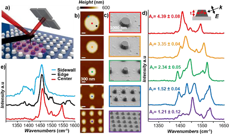
a) Schematic of the PTIR experiment. A pulsed tunable IR laser illuminates the portion of the sample (region highlighted in pink centered around gold-coated AFM probe operating in contact mode). b) AFM topography (scale bars 300 nm) and c) corresponding tilted SEM images (scale bars 1.0 μm) of five representative frustums with different aspect ratio. All the frustums have a thickness of 256 nm ± 4 nm. d) PTIR absorption spectra (p-polarization) obtained by positioning the AFM tip at the center of representative frustums, as indicated in panel b. The schematic of the incident polarization used for the measurements, along with the depiction of the quantities t and d, are provided as an inset. e) Color coded position dependent PTIR absorption spectra for the Ar = 4.39 frustum. The spectra in panel d) and e) are displayed with an offset for clarity.
The higher-l modes have many desirable properties. They are characterized by a shorter polariton wavelength λρ = 2π/q and hence, by a stronger field confinement that can be exploited for sub-diffraction imaging and focusing.19,22,30 Although many other higher-order HPhP modes (with m > 1 and n > 0) have been theoretically predicted,29 they remained elusive because coupling to far-field radiation is either very weak or forbidden by selection rules. These high-order HPhP modes offer more precise tailoring of the evanescent near-field spatial distributions and better matching of the polariton orbital angular momenta to those of nanoscale absorbers or emitters, potentially modifying the selection rules to make weak or forbidden transitions dominant.31,32
Scattering-type scanning-near-field optical microscopy (s-SNOM) utilizes a sharp, metallized tip as a scanning optical antenna that can aid the excitation of such modes in the near-field and has enabled imaging high-l modes in hBN slabs in real space.19,26 Here, we show that another near-field technique, photothermal induced resonance (PTIR), enables direct observation of multiple ‘limbs’ (m = 0,1; n = 0,1,2; l = 1,2,3,...) of the hBN hyperbolic dispersion relation in hBN frustum nanostructures. These measurements give the first unequivocal evidence for the existence of the ‘dark’ higher order modes.29 In previous far-field7 and s-SNOM20 measurements only the (l = 1,2,3,...) ‘branches’ of the m = 1, n = 0 limb were detected. PTIR makes the observation of the higher order modes possible because it detects light absorption by mechanically transducing the sample photothermal expansion, thus bypassing the challenge imposed by weak far-field emission that limits established methods. Consequently, these results highlight the PTIR capability to characterize nanophotonic dark-modes of both artificial meta18,33–37 and natural hyperbolic media.7,12,23–25,27,29
The PTIR method combines the spatial resolution of atomic force microscopy (AFM) with the specificity of absorption spectroscopy. Because PTIR often utilizes infrared (IR) excitation, it is also known as AFM-IR. Similar to s-SNOM, in PTIR a metallized AFM tip is used to overcome the momentum mismatch and/or enhance coupling between the far-field radiation and the deeply sub-diffraction polaritonic modes. In contrast to s-SNOM where the tip is operated in tapping mode and the scattered light is detected, in the PTIR experiments presented here, the AFM probe is in contact with the sample (contact mode) and acts as a near-field mechanical detector. A detailed comparison between the working principles of PTIR and s-SNOM and corresponding applications is available elsewhere.38
In PTIR, light incident on the tip excites confined polaritons, which eventually decay into incoherent lattice vibrations (heat). This causes a local thermal expansion of the sample, and in turn, the mechanical motion of the cantilever that is detected by the AFM position-sensitive detector.39 Although novel nanoscale probes with integrated cavity opto-mechanics,39 can track the fast sample thermal expansion dynamics, the conventional cantilevers used here are too slow to capture that process and are kicked into oscillation by the sample expansion similar to a struck tuning fork. Because the amplitude of the PTIR signal (cantilever oscillation) is proportional to the energy absorbed by the sample,40, 41 PTIR spectra enable mapping of electronic bandgap42 and chemical composition43 at the nanoscale, with applications in biology,44, 45 photovoltaics,46 polymer science,47, 48 pharmaceutics49 and plasmonics,50–52 as reviewed elsewhere.38, 53 For example, PTIR recently enabled the observation of ‘dark’ modes in plasmonic antennas50, 54 and the imaging of HPhPs modes in micrometer-sized hBN flakes.55
The PTIR set up used in this work consists of a wavelength-tunable, pulsed laser that illuminates a portion of the sample (≈ 50 μm diameter centered around the AFM probe) with an angle of ≈ 20° with respect to the sample surface (Fig. 1a). The gold-coated Si AFM probe provides the momentum-matching necessary for efficiently coupling the incident light into the highly confined, large-wavevector polaritonic modes. Five periodic arrays of hBN frustum-shaped nanostructures with d ranging from 312 nm ± 26 nm to 1120 nm ± 22 nm (as measured by AFM; Fig. 1b), similar to those previously measured by far-field reflectance/transmittance7 and s-SNOM,20 are studied here. The uncertainties in the nanostructure dimensions represent one standard deviation in the measurements of seven nominally identical structures. The nanostructures have a thickness of t = 256 nm ± 4 nm and are characterized by Ar ranging from 1.21 ± 0.12 to 4.39 ± 0.08, where the Ar uncertainty is determined by the uncertainty in the measurement of the frustum diameters. The corresponding scanning electron microscope (SEM) images are provided in Fig. 1c, with details on the sample fabrication available elsewhere.7,20 The hBN HPhP modes were observed within the hBN upper Reststrahlen band,7,12 which extends between the frequency of the in-plane longitudinal ωLO ≈ 1610 cm−1 and transverse optic phonons ωTO ≈ 1360 cm−1. Local PTIR absorption spectra (Fig. 1 d,e) were obtained for each cone by placing the AFM tip in specific locations on the frustums and plotting the amplitude of the cantilever-induced oscillations as a function of laser frequency. In addition, PTIR absorption maps were obtained by scanning the AFM tip while illuminating the sample at a given incident frequency and measuring the amplitude of the cantilever-induced oscillation as a function of tip location. PTIR experiments can be obtained with either s- (in plane) or p- polarized light. Because of the incident light angle, illumination with p-polarization provides both an in- and an out-of-plane electric field component, the latter being amplified by the larger vertical polarizability of the gold-coated AFM probe. All PTIR data provided in the main text were obtained using p-polarized light (inset of Fig. 1d) since this illumination condition provides the most interesting results. For completeness, PTIR data obtained with s-polarized light are available in the Supplemental Information (Figs. S2 and S3).
The PTIR spectra from the center of representative frustums (Fig. 1d) highlight a broad range of optical modes and a systematic mode dispersion as a function of Ar. Although some of these resonances appear to directly correlate to those previously observed in both far-field7 and s-SNOM20 measurements, several additional, strong modes are observed. Particularly, many of the strongest resonances are found at frequencies above ≈ 1550 cm−1 (i.e. above the m = 1, n = 0, l = 1 resonance for the smallest Ar frustums) and were not reported for any of the arrays in prior works. Because each of the modes observed in the PTIR spectra show a systematic dispersion with Ar, we deduce that these resonances are indeed HPhP resonance modes. Furthermore, in contrast with previous s-SNOM observations,20 PTIR spectra obtained at different locations on a given frustum (see Fig. 1e) display clear spectral variations. This is most likely related to the the AFM tip efficiency in launching HPhPs while it is in contact with the frustum and the increased PTIR sensitivity for bulk modes, rather than relying on the launching of the HPhPs by the sharp frustum corners as was previously reported.6,20
The Fourier-Transform Infrared (FTIR) reflection spectrum for the Ar = 2.34 frustrum (Fig. 2a bottom panel) is dominated by a strong resonance at 1494 cm 1 along with two weaker resonances located at 1413 cm−1 and 1384 cm−1. These modes have been previously identified and assigned as where the subscripts are the modal indices m = 1 and l = 1, 2, 3, respectively, with the ‘U’ superscript referring to the upper Reststhralen band. The corresponding resonances were identified at ≈ 1491 cm−1, ≈ 1414 cm−1 and ≈ 1389 cm−1 within the PTIR spectrum (Fig. 2b bottom panel). We note that because the HPhPs in the upper Reststrahlen band with m = 0 and/or radial index n > 0 cannot be directly stimulated or measured in the far-field, the radial quantum number n (formerly denoted r) was ignored in previous work.7 Hereafter, all three quantum numbers, l, m, and n are used to describe the broad range of additional modes observed in the PTIR experiments,. Consequently, the previously observed resonances in hBN nanostructures correspond to the (lmn) = (l10) modes in the notation used here. The assignment and spectral positions for the first three branches of the (l10) limb match well between the experimental PTIR and far-field reflection data (Fig. 3b), as well as with resonances calculated for spheroidal nanoparticles (Fig. 3a). Although the structures discussed here are not spheroidal, an analytical solution for such particles29 previously provided a good qualitative description of the optical modes and the trends in the spectral dispersion with respect to changing Ar within frustum-shaped hBN nanoparticles.7 To clarify the meaning of the modal indexes (l, m, n), we calculated electric field intensity distributions along the x-direction (spheroid long axis ), shown in Fig. 4. As presented in a) l is the analog of the total orbital momentum within spherical harmonics, while b) m is the angular momentum in the azimuthal direction of the spheroid. Thus, the quantity l−m identifies the number of nodes of the potential observed along the colatitude angle π (see green inset). The index n counts the number of nodes of the electric potential in the radial direction. Therefore, n = 0 corresponds to surface modes, while n > 0 to those confined more within the bulk (Fig 4c). As only HPhP modes with n = 0 were detected by s-SNOM,20 this may imply that the sensitivity of the PTIR method to the bulk of the nanostructure may be needed to image such modes.
Fig. 2:
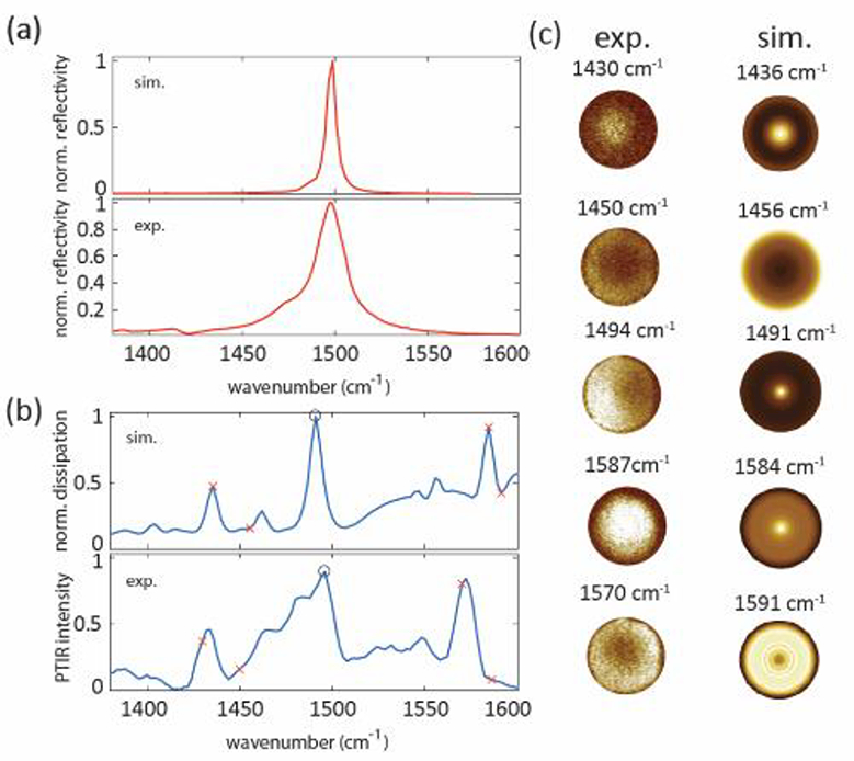
Simulated (top) and experimental (bottom) a) far-field reflectance and b) PTIR absorption spectra from the Ar = 2.34 frustum. c) PTIR absorption maps for the spectral position labeled (1 to 5) in panel b). d) Corresponding calculated PTIR maps obtained by integrating the power loss over the frustum volume for each position of the point dipole (50 nm above the frustum surface) that simulate the tip position in the PTIR experiments.
Fig. 3:
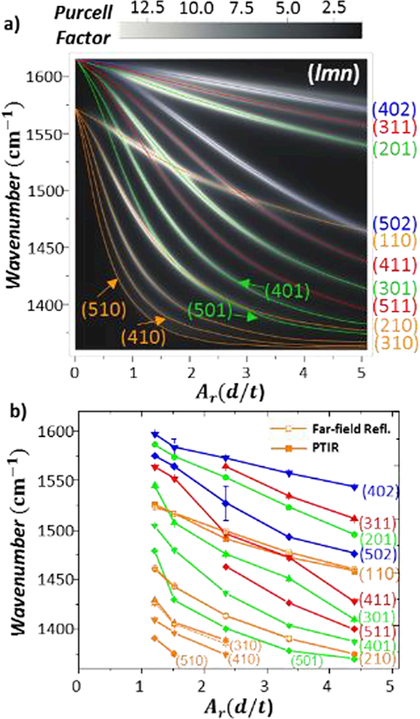
a) Analytical calculations of the HPhP dispersion for hBN ellipsoidal particles as a function of the Ar. Four specific ‘limbs’ are observed with multiple dispersing polaritonic modes. The grayscale represents the corresponding Purcell factor, while the colored lines are provided as a guide to the eye and identify the (l10) (orange traces), (l11) (red traces), (l01) (green traces) and (l02) (blue traces) limbs of the Αr.-dependent HPhP dispersion for hBN ellipsoidal particles. b) PTIR (full symbols) and FTIR (open symbols) experimental Αr-dependent dispersion from each of the five frustums measured in Fig. 1b. The modal assignments are in good qualitative agreement with the analytical calculations. The color lines and symbols, along with the (lmn) designations are provided for easier comparison with the calculations. The dispersion of the three observed resonances within the far-field reflection are also provided as the open circles and correspond to the (110), (210) and (310) branches. The error bars represent a single standard deviation of the resonance peak position uncertainties determined by the least-squares fitting algorithm. Some uncertainties are smaller than the dot size.
Fig. 4:
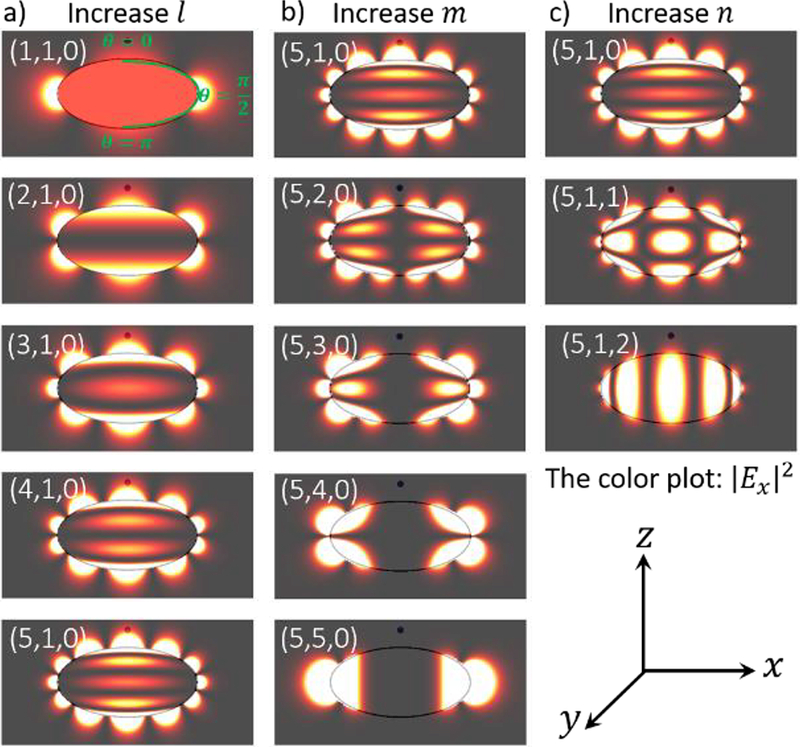
Schematic depiction of the evolution of the HPhP modes within spheroidal nanoparticles. The corresponding indices (l, m, n) are modified with the other two in each successive column, a) With increasing l, we see that the number of nodes in the electric field amplitude along the 𝜃 direction (see green inset) increases, with this being equal to the quantity l−m. b) For increasing m, the number of nodes in the azimuthal direction is increased, c) Finally, with increasing n, we see that that the number of nodes in the radial direction (from the spheroidal centroid to the surface) increases. Specifically, n = 0 is defined as a purely surface mode, while n > 0 implies volume-confinement.
The extension of the analytical calculations beyond the (l10) case to include those with m = 0 and n > 0 in the upper Reststrahlen band, offers a rich and complex dispersion relationship (see Fig. 3a). Here, the hyperbolic dispersion is represented as a function of Ar with the gray-scale corresponding to the calculated Purcell factor for the mode. To limit the complexity of the plots, only HPhPs with m = 0,1 and n = [(l — m)/2] ≤ 2 are given. In Fig 3a, we observe a series of limbs each corresponding to different m and/or n. Each limb is composed of several branches of varying l, with each limb designated by solid lines of the same color in Fig 3a. The previously reported (l10) limb is highlighted in orange. The previously unreported limbs [(l02); blue], [(l11); red], and [(l01); green] are also included. We now compare these theoretical curves with the experimental PTIR observations. Close examination of the PTIR spectra for each Ar demonstrates several series of dispersing resonant modes. Using the dispersion plot in Fig. 3a as a guide we can assign and group the resonance modes experimentally observed within the PTIR spectra into corresponding limbs and branches (Fig. 3b) that qualitatively match the analytical calculations (Fig 3a). We employ least-squares fitting of the resonances in the PTIR spectra (representative fit results are provided in Fig. S5 of Supplemental Information) to extract the reported resonance positions. While the sheer number of resonant modes observed in the PTIR spectra makes the unambiguous identification of each resonance challenging, the good qualitative agreement between the experimentally observed and calculated modes in terms of the Ar-dependence supports our assignments. The dependences are monotonic and allow for a straightforward ordering of the modes. Only for Ar values near the level crossings [e.g. (110) and (411) near 1500 cm−1 and Ar~3] are such assignments questionable. These assignments are supported further by the strong agreement between the resonance positions of the (l10) branch that were extracted from the PTIR (closed orange symbols in Fig. 3b) and the corresponding far-field reflection spectra (open orange symbols in Fig. 3b). Thus, all the modes within each of the spectra can be accounted for using these lowest order subsets of the HPhP limbs/branches that we took into consideration. Regardless of the specific assignments, our analysis clearly demonstrates that the additional resonances observed here are consistent with those previously anticipated by theory,29 including the modes occurring at frequencies higher than the frequency of the (l10) mode. As noted above, with the exception of the (l10) limb, the hBN resonances have not been experimentally observed previously owing to the limitations imposed by the far-field selection rules, thereby highlighting the power of the PTIR technique for nanophotonic modal observation and analysis.
In PTIR, the tip should launch polariton modes with roughly the same efficiency as in s-SNOM. However, our results indicate that in practice the PTIR can be advantageous to the s-SNOM for measuring dark modes due to the higher signal-to-noise ratio. This may be because the PTIR, unlike the s-SNOM, does not require subtraction of a large far-field background for extracting the near-field information. Contact-mode measurement in the PTIR vs. tapping-mode operation of the s-SNOM might be another reason why the former yields a stronger coupling to highly confined dark modes.
Electromagnetic simulations based on the finite-element method (FEM) offer further insight into the origin of the polaritonic resonances observed in the PTIR measurement. First, a simulation of plane-wave scattering from a frustum with Ar = 2.34 is performed (see Methods for details) and yields the reflection spectrum (Fig. 2a, top panel) where the prominent peak at 1491 cm−1 corresponds to the bright (110) resonance, in good agreement with the FTIR spectrum. Importantly, the additional polariton resonances detected in the PTIR measurement are not observed in the simulated reflection spectrum, reinforcing our postulate that they are due to polaritonic modes inaccessible by far-field excitation. We next performed a series of FEM simulations in which the same frustum was illuminated by a radiating electric dipole located 50 nm above the top surface. As we show next, this procedure emulated the presence of the AFM tip in the PTIR experiment, leading to the excitation of polariton waves through high-spatial-frequency electromagnetic-field components localized at the launching point. From steady-state field solutions to the dipole simulations, we obtained the electromagnetic power loss in the frustum, which we assumed to lead to an isotropic expansion of the geometry, proportional to the PTIR signal (details in the Methods and discussion below). Following this procedure for a dipole located at the center of the frustum, we obtained the dissipation spectrum shown in the top panel of Fig. 2b that is qualitatively well-matched to the PTIR spectrum obtained with the tip at the center of the Ar = 2.34 frustum (Fig. 2b, bottom panel). Specifically, prominent peaks and valleys labeled 1 to 5 are observed at roughly the same frequencies in both the PTIR and calculated spectra, indicating that the radiating dipole excites approximately the same polariton resonances as the PTIR tip.
A series of PTIR absorption maps (Fig. 2c) reveal the evolution of the HPhP near-field distributions for the frustum nanostructures with Ar = 2.34 as a function of frequency. The corresponding PTIR maps for the frustums with different Ar are provided in the Supplemental Information, Fig S6. As reported previously, the polariton near-field patterns exhibit a continuous evolution with respect to frequency, due to the frequency-dependent polariton propagation angle. Consequently, the field profiles that give rise to the PTIR absorption maps are decoupled from the resonances themselves, thereby providing an opportunity to tailor the near-field amplitude and the spatial distribution of the HPhP mode with nanostructure design. However, because the near-field patterns are not unique to a specific resonance they should not be directly labeled as such. The observed patterns are the result of strong localized absorption occurring at spatial locations where the ray-like trajectory29 of the HPhPs launched by the PTIR tip intersects with the exposed surface of the frustum. Although a spatial resolution as high as 20 nm56 has been reported for contact-mode PTIR experiments, it is also known that the PTIR spatial resolution is somewhat dependent on the sample thermomechanical properties.38,57 The PTIR images in this work were recorded with a horizontal pixel resolution between 6 nm and 3.2 nm depending on the scan size (see Methods). However, we estimate the spatial resolution to be of the order of 35 nm, determined from the sharpest features observed in the PTIR maps, i.e. comparable to the tip size. Such high-spatial resolution is somewhat surprising considering the high in-plane thermal conductivity of hBN and the relatively short lifetime of hBN HPhPs (< 10 ps), that is much shorter than the laser-pulse length used in the PTIR experiments (≈ 500 ns). Given these conditions, one would expect that the sample would thermalize within the duration of the laser pulse, leading to a homogeneous signal with an intensity proportional to the sample thickness, as is the case for experiments with s-polarization (Supplemental Information), or for modes coupling to the far-field. The heterogeneities in the PTIR maps with p-polarization (Fig. 2c and Fig. S6) are interpreted to reflect the location-specific coupling efficiency between the free-space wavelength and the HPhPs mediated by the AFM-probe. In other words, given an incident frequency, the gold-coated tip couples light efficiently to the nanostructure only at locations where the corresponding HPhP near-fields are strong. The hBN nanostructure still thermalizes within the 500 ns long laser pulse; however, the amount of absorbed energy (PTIR intensity) is proportional to the local light-matter coupling strength.
Note that the Purcell factor was originally introduced in photonics to characterize the power dissipation of a dipole emitter in a cavity. Recently, this quantity has been used as a good figure of merit for light-matter interactions in polaritonic systems.6,7,29,58,59 As the AFM tip can, at some very crude level, be approximated by a point emitter and since the power dissipation is the key ingredient of the PTIR response, we speculate that the Purcell factor could be correlated with the PTIR signal. Unfortunately, the quantitative relationship between the PTIR amplitude and the Purcell factor is difficult to determine. Such a task would require a realistic modeling for the tip-sample coupling, the nanostructure thermal expansion, and the cantilever dynamics60, which is beyond the scope of this work.
Electromagnetic simulations using dipole-excitation were also employed in an attempt to replicate and understand these features in the PTIR absorption maps. For this purpose, the dipole excitation source, at selected wavenumbers, was scanned across the frustum top surface. At each location, the total electromagnetic power loss in the nanostructure was calculated (details in the Methods). The calculations are restricted to the frustum top surface because they could not easily provide information for the nanostructure sidewalls. The calculated electromagnetic power loss maps in Fig. 2d are qualitatively similar to the corresponding PTIR images in Fig. 2c (see Fig. S6 for the PTIR images that include the frustum sidewall) and exhibit a gradually changing absorption profile. A distinguishing feature of both the experimental and calculated data sequence is the frequency-dependent evolution of the absorption distribution. It alternates between featuring a maximum near the center of the frustum (‘1’, ‘3’, ‘4’ in Fig. 2c) and a donut-shape with a minimum at the center (‘2’ and ‘4’ in Fig. 2c). These maps, along with the dependence of the PTIR spectra with probe position (Fig. 1e) imply that the AFM probe plays a significant role in the launching of the polaritons within the PTIR experiment. This is in direct contrast to s-SNOM measurements where the presence of the tip induces a minor perturbation to the dielectric environment. Calculations of the cross-sectional electric field, together with the corresponding power flux profiles obtained with the dipole source fixed 50 nm above the center of the frustum top-surface highlight trajectories of the polaritonic rays as a function of the frequency (Fig. 5). As demonstrated by Caldwell et al. and Giles et al., 20 the frequency dependent propagation angle (π) with respect to the z-axis within these frustums is dictated by the hyperbolic polariton propagation condition:
| (2) |
where the subscripts t and z designate the in-plane and the out-of-plane axes of the crystal, respectively, and 𝜀j is the frequency-dependent dielectric function (permittivity) of the material along the y-axis. At the principal (110) resonance frequency (1494 cm−1, Fig. 5b), it is apparent that the power flux from the dipole emitter propagates at the anomalous angle 𝜃 to the lower corner of the frustum, then returns back to the center of the top surface. Below 1494 cm’1 (i.e. at 1430 cm−1, Fig. 5a), a similar power flow pattern is observed, except that the larger propagation angle leads to the HPhP reflection at the frustum sidewall. These types of HPhP trajectories were described previously by Caldwell et al. 7 and observed experimentally via s-SNOM in higher aspect-ratio frustums.20 However, above the 1494 cm−1 principal mode, (e.g., at 1591cm−1, Fig. 5c) the power flows at a smaller angle 𝜃, leading to polariton reflections against the frustum’s top and bottom surfaces. This effect has not been observed previously and is characterized by a Poynting vector predominantly oriented in the transverse direction, in contrast with the longitudinal (z-axis) direction of the previous cases. This wide variation in the power-flow direction could be exploited in hBN applications; for example, it could impact the coupling between the HPhPs and local emitters placed next to the hBN nanostructures. For instance, this could provide an amplification of IR-active vibrational resonances for local molecules intercalated between the hBN layers through the surface-enhanced IR absorption (SEIRA) effect, analogous to recent demonstrations using evanescent fields of HPhPs.61 We note that the resonances shown in Fig. 5 are supported in frustums of different Ar, albeit with spectrally shifted frequencies (Fig. S7 of the SI shows the cross-sectional electric-field magnitude and Poynting vector plots for resonances of frustums with four different aspect ratios).
Fig. 5:
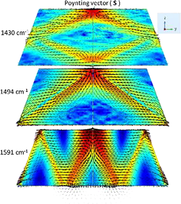
Three dimensional electromagnetic calculations of the cross sectional electromagnetic field amplitude for a frustum with Ar =2.3 illuminated by an electric point dipole located the center of the frustum, 50 nm above the top surface, at 1436 cm−1 (top), 1491 cm−1 (middle) and 1591 cm−1 (bottom). The overlaid arrows designate the Poynting vector (S) for the polaritonic modes. Note that the direction of the field cycling and thus the predominant direction of the Poynting vector are reversed between frequencies lower (1430 cm−1) and above (1591 cm−1) the principle (110) resonance of the hBN frustum.
In summary, the PTIR technique was used here to provide the first observation of non-radiative HPhPs modes in hBN, enabling the detection of up to five branches of four different limbs of the Ar-dependent hyperbolic dispersion relationship. Such non-radiative modes were predicted theoretically,29 however, their far-field selection rules have precluded their direct observation in previous experiments. The PTIR near-field technique, mediated by the sample thermal expansion, enables the detection of these dark HPhP modes. The comparison of the rich PTIR spectra with the calculations of the Ar-dependent dispersion for spheroidal nanoparticles, for which an analytical solution is available, provided the basis for the assignment of the quantum numbers defining each limb and branch to the experimentally observed modes and their Ar-dependent dispersion. The PTIR absorption maps also enabled the visualization of the frequency-dependent evolution of the local resonant absorption that closely mirrors the trends observed in electromagnetic near-field simulations. Such simulations indicate that the power-flow trajectories of confined HPhP rays are a strong function of frequency. This suggests that the local near-field emission profile and/or the propagation properties of a hyperbolic waveguide can be directly modified through local nanostructure design in a manner that is decoupled from control of the individual polariton frequencies. More broadly, these results also highlight the capabilities of the PTIR method in characterizing nanophotonic materials and nanostructures that are complementary to the more traditional techniques such as far-field reflection/transmission spectroscopy and s-SNOM.
Methods
Sample Fabrication
The hBN crystals were grown using a high-pressure/high-temperature method62,63 and were exfoliated and transferred onto a quartz substrate. The flake thickness was initially measured via atomic force microscopy and measured again after the fabrication of the frustums. The sample was coated with a bilayer of PMMA and patterned with electron beam lithography using an Al hard mask created via electron-beam evaporation and liftoff. The hBN nanostructures were fabricated via reactive ion etching in an oxygen environment. The remaining metal was then removed with wet chemical etchants. Further details of the fabrication process can be found in the literature.7,20
PTIR measurements
PTIR spectra and images were obtained with a commercial PTIR instrument interfaced with a quantum cascade laser tunable from 1934 cm−1 (5.17 μm) to 1126 cm−1 (8.88 μm) that illuminates the sample at ≈ 20° from the sample plane. The laser repetition rate was set to 1 kHz and the pulse length to 500 ns (0.05 % duty cycle); the laser spot size at the sample was ≈ 50 μm in diameter. PTIR spectra were obtained by averaging the cantilever deflection amplitude from 512 individual laser pulses at each wavelength and tuning the laser at intervals of 2 cm−1. Up to four spectra were acquired and averaged for each tip location, and smoothed by considering 7 adjacent points (see Fig. S7 for the comparison between smoothed and unsmoothed data). AFM topography and PTIR maps were acquired simultaneously illuminating the sample at constant wavelength, by synchronizing the signal acquisition so that the PTIR signal in each pixel was an average over 32 laser pulses.40 All PTIR and topography images were obtained with a 0.06 Hz scan rate over a areas ranging from 0.8 μm × 0.8 μm to 1.5 μm × 1.5 μm depending on the nanostructure size (i.e. probe velocity between 50 nm/s and 100 nm/s). The images are composed of 250 pixels in the horizontal direction and 100 pixels in the vertical direction, that yield a horizontal pixel resolution of 6 nm, 5 nm, 4 nm, and 3.2 nm for the frustum with Ar =4.39, 3.35, 2.34, and 1.52, respectively. All PTIR experiments were obtained using p-polarization unless otherwise noted. Commercially available 450 μm long gold-coated silicon contact-mode AFM probes with a nominal spring constant between 0.07 N/m and 0.4 N/m were used for all the PTIR experiments.
Electromagnetic Simulations
Theoretical FTIR Reflection Spectrum.
The theoretical FTIR reflection spectrum shown in the top panel of Fig. 2(a) was obtained with a finite-element based simulation of a plane-wave scattering against a hBN truncated cone (frustum) with height 265 nm and bottom and top diameter of 510 nm and 710 nm respectively (Ar = 2.3), sitting on top of a substrate with refractive index 1.2069 (i.e. quartz). The complex permittivity of the hBN frustum was the same as in ref. 7. A scattered-wave formulation was adopted, in which the solution of a p-polarized plane wave scattering against the planar air-quartz interface at a 20° angle from the sample surface was used to excite the frustum. The intensity of the frustum-scattered field, normalized to the incoming plane wave intensity, was determined to yield the simulated FTIR reflection spectrum.
Theoretical PTIR Spectrum.
The theoretical PTIR spectrum (Fig. 2b) was calculated via a finite-element method simulation of an electric point dipole radiating 50 nm above the center of the frustum, and oriented normally to its top surface. Perfectly-matched layers (PMLs) surrounded by the frustum in order to emulate open domains in all directions. The steady-state electric field (E) inside the frustum, and the electromagnetic power loss per unit volume (Qh = 2πf ε0ε”|Ε|2) were obtained in the spectral range between 1380 cm−1 and 1600 cm−1 (here f is the frequency, ε0 is the vacuum permittivity and έ’ is the imaginary part of the complex hBN permittivity). The normalized calculated PTIR spectrum in Fig. 2(b) was obtained integrating Qh over the volume of the entire frustum based on the assumption that the expansion of the frustum is isotropic and proportional to Qh. The choice of 50 nm dipole distance from the frustum surface is justified by the fact that it maximized the visibility of the prominent features in simulation in most cases.
Theoretical PTIR Images.
The theoretical PTIR maps (Fig. 2c) were obtained by calculating the total electromagnetic power loss Qh in the hBN cone (as discussed above), at selected wavenumbers for dipole positions varying across the entire frustum top surface.
Analytical Calculations
The hBN nanoparticle was modeled by a spheroid. Its polaritonic eigenmodes were found solving numerically the transcendental equation given in previous work. (Note the small difference in notations: the mode indices l, m, n here correspond to l, m, r in Refs. 7 and 29). We represent the AFM tip by a point dipole emitter placed above the north pole of the spheroid. The dipole axis is specified by a unit vector d, which we chose to be 45 degrees with respect to the equatorial plane of the spheroid plane of the spheroid. We assume that the PTIR signal is proportional to the Purcell factor of the emitter, f = 1 + (3/2)(𝜆0/2π)3Im(d ∙ E), where 𝜆0 is the vacuum wavelength of light and E is the reflected electric field at the dipole’s location. The calculation of the Purcell factor is performed by expanding E in spheroidal harmonics according to the formulas given in the Supplementary Material of Ref. 29.
Supplementary Material
Acknowledgements
L.V.B. acknowledges support under the Cooperative Research Agreement between the University of Maryland and the National Institute of Standards and Technology Center for Nanoscale Science and Technology, Award 70NANB14FI209, through the University of Maryland. J.D.C., I.V. and A.J.G. were funded by the Office of Naval Research (ONR) with the funds distributed by the Nanoscience Institute at the Naval Research Laboratory. N.S. acknowledges the support of the National Research Council (NRC)/NRL Postdoctoral Fellowship Program. A.V.K. and K.S.N. acknowledge support from the EPSRC (U.K.), the Royal Society (U.K.), European Research Council, and the EC-FET European Graphene Flagship. M.M.F. and Z.S. were supported by the Office of Naval Research under Grant N00014–15-1–2671, by the National Science Foundation under Grant No. ECCS-1640173, and by the Semiconductor Research Corporation (SRC) through the SRC-NRI Center for Excitonic Devices, research 2701.002. K.W. and T.T. acknowledge support from the Elemental Strategy Initiative conducted by the MEXT, Japan and JSPS KAKENHI Grant Numbers JP15K21722. S.A.M. acknowledges ONR Global, the EPSRC Reactive Plasmonics Programme EP/M013812/1, and the Lee-Lucas Chair in Physics
REFERENCES
- 1.Caldwell JD; Lindsey L; Giannini V; Vurgaftman I; Reinecke T; Maier SA; Glembocki OJ Nanophotonics 2014, 4, 44–68. [Google Scholar]
- 2.Greffet J-J; Carminati R; Joulain K; Mulet JP; Mainguy SP; Chen Y Nature 2002, 416, (6876), 61–64. [DOI] [PubMed] [Google Scholar]
- 3.Hillenbrand R; Taubner T; Keilmann F Nature 2002, 418, (6894), 159–162. [DOI] [PubMed] [Google Scholar]
- 4.Schuller JA; Taubner T; Brongersma ML Nature Photonics 2009, 3, 658–661. [Google Scholar]
- 5.Wang T; Li P; Chigrin DN; Giles AJ; Bezares FJ; Glembocki OJ; Caldwell JD; Taubner T ACS Photonics 2017, 4, (7), 1753–1760. [Google Scholar]
- 6.Caldwell JD; Glembocki OJ; Sharac N; Long JP; Owrutsky JO; Vurgaftman I; Tischler JG; Bezares FJ; Wheeler V; Bassim ND; Shirey L; Francescato Y; Giannini V; Maier SA Nano Lett 2013, 13, (8), 3690–3697. [DOI] [PubMed] [Google Scholar]
- 7.Caldwell JD; Kretinin AV; Chen Y; Giannini V; Fogler ΜM; Francescato Y; Ellis CT; Tischler JG; Woods CR; Giles AJ; Hong M; Watanabe K; Taniguchi T; Maier SA; Novoselov KS Nature Communications 2014, 5, 5221. [DOI] [PubMed] [Google Scholar]
- 8.Chen Y; Francescato Y; Caldwell JD; Giannini V; Maß TWW; Glembocki OJ; Bezares FJ; Taubner T; Kasica R; Hong M; Maier SA ACS Photonics 2014, 1, (8), 718–724. [Google Scholar]
- 9.Feng K; Streyer W; Islam SM; Verma J; Jena D; Wasserman D; Hoffman AJ Appl. Phys. Lett 2015, 107, 081108. [Google Scholar]
- 10.Wang T; Li P; Hauer B; Chigrin DN; Taubner T Nano Lett 2013, 13, (11), 5051–5055. [DOI] [PubMed] [Google Scholar]
- 11.Razdolski I; Chen Y; Giles AJ; Gewinner S; Schollkopf W; Hong M; Wolf M; Giannini V; Caldwell JD; Maier SA; Paarmann A Nano Lett. 2016, 16, 6954–6959. [DOI] [PubMed] [Google Scholar]
- 12.Dai S; Fei Z; Ma Q; Rodin AS; Wagner M; McLeod AS; Liu ΜK; Gannett W; Regan W; Thiemens M; Dominguez G; Castro Neto AH; Zettl A; Keilmann F; Jarillo-Herrero P; Fogler ΜM; Basov DN Science (Wash.) 2014, 343, (6175), 1125–1129. [DOI] [PubMed] [Google Scholar]
- 13.Dai S; Ma Q; Liu ΜK; Andersen T; Fei Z; Goldflam M; Wagner M; Watanabe K; Taniguchi T; Thiemens M; Keilmann F; Janssen GCAM; Zhu S-E; Jarillo-Herrero P; Fogler MM; Basov DN Nat. Nanotechnol 2015, 10, 682–686 [DOI] [PubMed] [Google Scholar]
- 14.Kumar A; Low T; Fung KH; Avouris P; Fang NX Nano Lett. 2015, 15, (5), 3172–3180. [DOI] [PubMed] [Google Scholar]
- 15.Woessner A; Lundeberg MB; Gao Y; Principi A; Alonso-Gonzalez P; Carrega M; Watanabe K; Taniguchi T; Vignale G; Polini M; Hone J; Hillenbrand R; Koppens FH L. Nat. Mater 2014, 14, 421–425. [DOI] [PubMed] [Google Scholar]
- 16.Caldwell JD; Vurgaftman I; Tischler JG; Glembocki OJ; Owrutsky JC; Reinecke TL Nature Nanotechnology 2016, 11, 9–15. [DOI] [PubMed] [Google Scholar]
- 17.Caldwell JD; Novoselov KS Nat. Mater 2015, 14, 364. [DOI] [PubMed] [Google Scholar]
- 18.Poddubny A; Iorsh I; Belov P; Kivshar Y Nature Photonics 2013, 7, 948–957. [Google Scholar]
- 19.Dai S; Ma Q; Andersen T; McLeod AS; Fei Z; Liu MK; Wagner M; Watanabe K; Taniguchi T; Thiemens M; Keilmann F; Jarillo-Herrero P; Fogler MM; Basov DN Nature Communications 2015, 6, 6963. [DOI] [PMC free article] [PubMed] [Google Scholar]
- 20.Giles AJ; Dai S; Glembocki OJ; Kretinin A; Sun Z; Ellis CT; Tischler JG; Taniguchi T; Watanabe K; Fogler MM; Novoselov KS; Basov DN; Caldwell JD Nano Lett. 2016, 16, (6), 3858–3565. [DOI] [PubMed] [Google Scholar]
- 21.Ishii S; Kildishev AV; Narimanov EE; Shalaev VM; Drachev VP Laser and Photonics Reviews 2013, 7, 265–271. [Google Scholar]
- 22.Li P; Lewin M; Kretinin AV; Caldwell JD; Novoselov KS; Taniguchi T; Watanabe K; Gaussmann F; Taubner T Nature Communications 2015, 6, 7507. [DOI] [PMC free article] [PubMed] [Google Scholar]
- 23.Korzeb K; Gajc M; Pawlak DA Opt. Express 2015, 23, (20), 25406–25424. [DOI] [PubMed] [Google Scholar]
- 24.Low T; Chaves A; Caldwell JD; Kumar A; Fang NX; Avouris P; Heinz TF; Guinea F; Martin-Moreno L; Koppens FH L. Nature Materials 2017, 16, 162–194. [DOI] [PubMed] [Google Scholar]
- 25.Sun J; Litchinitser NM; Zhou J ACS Photonics 2014, 1, (4), 293–303. [Google Scholar]
- 26.Giles AJ; Dai S; Vurgaftman I; Hoffman T; Liu S; Lindsay L; Ellis CT; Assefa N; Chatzakis I; Reinecke TL; Tischler JG; Fogler MM; Edgar JH; Basov DN; Caldwell JD Nature Materials 2017, doi: 10.1038/nmat5047. [DOI] [PubMed] [Google Scholar]
- 27.Xu GX; Ghamsari BG; Jiang J-H; Gilburd L; Andreev GO; Zhi C; Bando Y; Golberg D; Berini P; Walker GC Nature Communications 2014, 5, 4782. [DOI] [PubMed] [Google Scholar]
- 28.Yoxall E; Schnell M; Nikitin AY; Txoperena O; Woessner A; Lundeberg MB; Casanova F; Hueso LE; Koppens FHL; Hillenbrand R Nature Photonics 2015, 9, 674–678. [Google Scholar]
- 29.Sun Z; Gutierrez-Rubio A; Basov DN; Fogler MM Nano Lett. 2015, 15, (7), 4455–4460. [DOI] [PubMed] [Google Scholar]
- 30.Liu Z; Lee H; Xiong Y; Sun C; Zhang X Science (Wash.) 2007, 315, 1686-. [DOI] [PubMed] [Google Scholar]
- 31.Rivera N; Kaminer I; Zhen B; Joannopoulos JD; Soljacic M Science (Wash.) 2016, 353, (6296), 263–269. [DOI] [PubMed] [Google Scholar]
- 32.Machado F; Rivera N; Buljan H; Soljacic M; Kaminer I condmat 2017, 1610.01668v2. [Google Scholar]
- 33.Yang X; Yao J; Rho J; Xiaobo Y; Zhang X Nature Photonics 2012, 6, 450–453. [Google Scholar]
- 34.Guo Y; Newman W; Cortes CL; Jacob Z Advances in OptoElectronics 2012, 2012, 452502. [Google Scholar]
- 35.Noginov M; Lapine M; Podolskiy VA; Kivshar Y Opt. Express 2013, 21, (12), 14895–14897. [DOI] [PubMed] [Google Scholar]
- 36.Jacob Z Nat. Mater 2014, 13, 1081–1083. [DOI] [PubMed] [Google Scholar]
- 37.Hoffman AJ; Alekseyev L; Howard SS; Franz KJ; Wasserman D; Podolskiy VA; Narimanov EE; Sivco DL; Gmachl C Nature Materials 2007, 6, (12), 946–950. [DOI] [PubMed] [Google Scholar]
- 38.Centrone A Annu. Rev. Anal. Chem 2015, 8, (1), 101–126. [DOI] [PubMed] [Google Scholar]
- 39.Chae J; An S; Ramer G; Stavila V; Holland G; Yoon Y; Talin AA; Allendorf M; Aksyuk VA; Centrone A Nano Lett. 2017, 17, (9), 5587–5594. [DOI] [PMC free article] [PubMed] [Google Scholar]
- 40.Lahiri B; Holland G; Centrone A Small 2013, 9, (3), 439–445. [DOI] [PubMed] [Google Scholar]
- 41.Tang F; Bao P; Su Z Anal. Chem 2016, 88, (9), 4926–4930. [DOI] [PubMed] [Google Scholar]
- 42.Chae J; Dong Q; Huang J; Centrone A Nano Lett. 2015, 15, (12), 8114–21. [DOI] [PMC free article] [PubMed] [Google Scholar]
- 43.Katzenmeyer AM; Canivet J; Holland G; Farrusseng D; Centrone A Angew. Chem. Int. Ed 2014, 53, (11), 2852–2856. [DOI] [PubMed] [Google Scholar]
- 44.Ruggeri FS; Longo G; Faggiano S; Lipiec E; Pastore A; Dietler G Nat Commun 2015, 6, 7831. [DOI] [PMC free article] [PubMed] [Google Scholar]
- 45.Baldassarre L; Giliberti V; Rosa A; Ortolani M; Bonamore A; Baiocco P; Kjoller K; Calvani P; Nucara A Nanotechnology 2016, 27, (7), 075101. [DOI] [PubMed] [Google Scholar]
- 46.Strelcov E; Dong Q; Li T; Chae J; Shao Y; Deng Y; Gruverman A; Huang J; Centrone A Sci Adv 2017, 3, (4), e1602165. [DOI] [PMC free article] [PubMed] [Google Scholar]
- 47.Ghosh S; Kouame NA; Ramos L; Remita S; Dazzi A; Deniset-Besseau A; Beaunier P; Goubard F; Aubert P-H; Remita H Nat. Mater 2015, 14, (5), 505–511. [DOI] [PubMed] [Google Scholar]
- 48.Morsch S; Liu YW; Lyon SB; Gibbon SR Acs Applied Materials & Interfaces 2016, 8, (1), 959–966. [DOI] [PubMed] [Google Scholar]
- 49.Van Eerdenbrugh B; Lo M; Kjoller K; Marcott C; Taylor LS Mol. Pharm 2012, 9, (5), 1459–1469. [DOI] [PubMed] [Google Scholar]
- 50.Lahiri B; Holland G; Aksyuk V; Centrone A Nano Lett. 2013, 13, (7), 3218–3224. [DOI] [PubMed] [Google Scholar]
- 51.Chae J; Lahiri B; Centrone A Acs Photonics 2016, 3, (1), 87–95. [DOI] [PMC free article] [PubMed] [Google Scholar]
- 52.Khanikaev AB; Arju N; Fan Z; Purtseladze D; Lu F; Lee J; Sarriugarte P; Schnell M; Hillenbrand R; Belkin MA; Shvets G Nat. Commun 2016, 7. [DOI] [PMC free article] [PubMed] [Google Scholar]
- 53.Dazzi A; Prater CB Chem. Rev 2017, 117, (7), 5146–5173. [DOI] [PubMed] [Google Scholar]
- 54.Katzenmeyer AM; Chae J; Kasica R; Holland G; Lahiri B; Centrone A Adv. Optical Mater 2014, 2, (8), 718–722. [Google Scholar]
- 55.Ambrosio A; Jauregui LA; Dai S; Chaudhary K; Tamagnone M; Fogler MM; Basov DN; Capasso F; Kim P; Wilson WL ACS Nano 2017, 11, (9), 8741–8746 [DOI] [PubMed] [Google Scholar]
- 56.Katzenmeyer AM; Holland G; Kjoller K; Centrone A Anal. Chem. (Wash.) 2015, 87, (6), 3154–3159. [DOI] [PubMed] [Google Scholar]
- 57.Dazzi A, PhotoThermal Induced Resonance. Application to Infrared Spectromicroscopy In Thermal Nanosystems and Nanomaterials, Volz S, Ed. Springer Berlin; 2009; Vol. 118, pp 469–503. [Google Scholar]
- 58.Kuttge M; Garcia de Abajo FJ; Polman A Nano Lett. 2010, 10, 1537–1541. [DOI] [PubMed] [Google Scholar]
- 59.Maier SA Opt. Express 2006, 14, 1957–1964. [DOI] [PubMed] [Google Scholar]
- 60.Ramer G; Aksyuk V; Centrone A Anal. Chem. (Wash.) 2017, 89, (24), 13524–13531. [DOI] [PMC free article] [PubMed] [Google Scholar]
- 61.Autore M; Li P; Dolado I; Alfaro-Mozaz FJ; Esteban R; Atxabal A; Casanova F; Hueso LE; Alonso-Gonzalez P; Aizpurua J; Nikitin AY; Velez S; Hillenbrand R Light: Science & Applications 2017, doi: 10.1038/lsa.2017.172. [DOI] [PMC free article] [PubMed] [Google Scholar]
- 62.Taniguchi T; Watanabe KJ Cryst. Growth 2007, 303, (2), 525–529 [Google Scholar]
- 63.Watanabe K; Taniguchi T; Kanda H Nature Materials 2004, 3, 404–409. [DOI] [PubMed] [Google Scholar]
Associated Data
This section collects any data citations, data availability statements, or supplementary materials included in this article.