Abstract
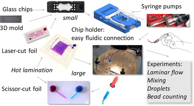
Lab-on-a-chip technology is brought into the classroom through development of a lesson series with hands-on practicals. Students can discover the principles of microfluidics with different practicals covering laminar flow, micromixing, and droplet generation, as well as trapping and counting beads. A quite affordable novel production technique using scissor-cut and laser-cut lamination sheets is presented, which provides good insight into how scientific lab-on-a-chip devices are produced. In this way high school students can now produce lab-on-a-chip devices using lamination sheets and their own lab-on-a-chip design. We begin with a review of previous reports on the use of lab-on-a-chip technology in classrooms, followed by an overview of the practicals and projects we have developed with student safety in mind. We conclude with an educational scenario and some initial promising results for student learning outcomes.
Keywords: Microscale Lab, High School/Introductory Chemistry, Undergraduate Research, Hands-On Learning/Manipulatives, Inquiry-Based/Discovery Learning, Laboratory Equipment/Apparatus, Nanotechnology, Public Understanding/Outreach, Interdisciplinary/Multidisciplinary
Introduction
The potential of using lab-on-a-chip devices in education has been explored using different devices and techniques depending on the learning goals and settings involved. Microfluidics lab-on-a-chip practicals can target understanding of microfluidics, measurement, and explanation, as well as incorporating design cycles in which students prototype and test their designs.1,2 Thus, microfluidics education can cover topics and skills in both science and engineering. In Table 1, an overview is given of prior articles and reports on the use of microfluidics practicals in secondary schools and undergraduate programs, showing the domains and concepts covered in those educational settings. The lab-on-a-chip devices described in these articles and reports were either ready-made, self-designed or even self-made using a variety of materials and techniques.
Table 1. Aspects of Lab-on-a-Chip and Microfluidics Practicals from the Literature.
| Aspect | Characteristic | Literature (see References; T = This Article) |
|---|---|---|
| School level | Secondary school | (2, 3, 13), T |
| Undergraduate courses | (1, 4−10, 13, 15), T | |
| Domain | Physics | (1, 2, 5, 11), T |
| Chemistry | (1−7, 10−14), T | |
| Biology | (2, 8, 10, 11, 13−15), T | |
| Engineering | (1−3, 10−12, 14), T | |
| Goal | Introduction to microfluidics | (1−3, 5, 10, 11, 13), T |
| Demonstration | (1, 2, 11, 12), T | |
| Design and engineering skills | (1−4, 10, 11, 13, 14), T | |
| Small-scale analysis and synthesis | (1−8, 12, 15) | |
| Concepts | Capillary flow | (1, 2, 11, 13), T |
| Laminar flow | (1−3, 5, 11), T | |
| Mixing | (1−4, 6, 10, 11, 14), T | |
| Droplet formation | (1, 2), T | |
| Measurement and detection | (1, 7), T | |
| Electrochemistry | (1) | |
| Chemical analysis | (1, 7, 12) | |
| Chemical synthesis | (3−6, 10), T | |
| Biological experiments on chip | (2, 8, 11, 13−15) |
Details about the different devices and techniques used can be found in Table 2. While many of these approaches address safety hazards,1−6,10,12 the long preparation times1−6,8,11,14 and requirement for skilled specialists1,2,8,14,15 can make their implementation cumbersome for schools. Rapid prototyping options are highly valued for the design and production of lab-on-a-chip solutions for design problems by students.
Table 2. Aspects of Devices Used for Lab-on-a-Chip Practicals from the Literature.
| Aspect | Characteristic | Literature (see References; T = This Article) |
|---|---|---|
| Device production | Ready-made | (1, 7, 11, 15), T |
| Self-designed | (1, 2, 11, 13, 14), T | |
| Self-made | (1−6, 8, 10, 11, 13), T | |
| Device material | Glass | (1, 4, 10, 12, 14, 15), T |
| PMMA (poly(methyl methacrylate)) | (1, 2, 7, 11) | |
| PDMS (polydimethylsiloxane) | (1−6, 8, 11−14) | |
| Gelatin | (12) | |
| Foil | T | |
| Paper | (11) | |
| Other | (2, 11, 13) | |
| Device technique | Lithography | (1, 2, 4, 8, 10−15), T |
| Etching | (1, 10, 12, 15), T | |
| Molding | (1−3, 7, 11, 12), T | |
| Milling | (1, 2, 11) | |
| Casting | (1−6, 8, 11, 12) | |
| Cutting | (1, 2, 11), T |
Design of the Lab-on-a-Chip Lesson Series
To increase familiarity with this frontier science area of microfluidics, a lesson series including hands-on practicals was designed for use in the classroom. This lesson series is part of a nationwide program in which upper secondary school students in The Netherlands, between 15 and 18 years old, engage with multidisciplinary science and engineering techniques as practiced in research and development in the field.16
A Teacher Development Team of high school teachers, scientists, and lab-on-a-chip specialists jointly developed the materials and hardware for the lesson series. The lesson series gives various examples of lab-on-a-chip applications from healthcare and veterinary medicine17−19 and provides an authentic context for learning. Learners are supported in working with real lab-on-a-chip equipment and performing experiments on basic principles of microfluidics: laminar flow, micromixing, and droplet generation. Additional equipment enables bead counting, bead sorting and trapping, and conductivity measurement. The written materials include practical manuals, theory, and exercises. Our design and selection of microfluidic equipment, complemented with experiments using low-cost foil and homemade chip holder, provide a variety of possibilities for school teachers to introduce microfluidic concepts and frontier lab-on-a-chip research topics.
Lab-on-a-Chip Practical Kit
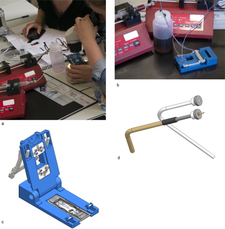
A custom chip holder was designed for use in the practicals (Figure 1). This chip holder uses standardized connections for fluidic chips and supports the use of other commercial or custom-made chips as well. For educational use, the chip holder was designed to permit quick and leak-free connection of fluidic chips. The practicals give students the opportunity to view and manipulate microfluidic chips and verify what is happening on the chip using a microscope.
Figure 1.
Educational lab-on-a-chip setup: (a) Learners using the lab-on-a-chip setup in the classroom. (b) The educational setup demonstrating laminar flow in the H-reactor (see Figure 2). (c) The design of the chip holder. (d) Detail showing the fluidic and electronic connectors.
To facilitate the implementation of the lesson series by schools, all equipment required for the lab-on-a-chip experiments was assembled in a lab-on-a-chip practical kit. These kits are borrowed by teachers for as long as the lesson series takes. In this way, costs for schools are limited, and maintenance is done with expert help. School teachers and technicians are trained in a 4 h session to conduct the microfluidic experiments, provided in a practical kit, in the classroom, which will help them implement the lesson series at school. Further outside expert help in the classroom is not necessary during the lesson series.
The practical kit includes chip holders (Figure 1), various fluidic chips (H-shaped microreactor, mixer, droplet generator, electric demo chip, bead counting and trapping chip), a number of lithium chips18 (nonfilled, for microscopy), two syringe pumps, polymer tubing, a tubing cutter, ferrules, various tubing connectors, syringes, dyed water, oil, detergent, a waste container, USB microscope, and table plates.
After testing at two schools (which did not participate in the development process), the lesson series passed the national certification criteria for use in the NLT curriculum (Nature, Life & Technology)16 at high schools in The Netherlands. The lesson series is currently used on a regular basis. The first schools started using the lesson series in 2012, and currently teachers and technicians at over 15 schools have implemented the lesson series, serving 15–60 students per school per year. Most teachers repeat the lesson series each year and help with improving its texts and practical equipment. Some school classes visit the outreach laboratory for additional practicals on lab-on-a-chip, or to present their student projects to university staff. Parts of the practical work are used in master classes, outreach activities, and workshops for students or adults. The practicals are also used in the chemistry and physics curriculum.
After the first schools started using the lesson series and the practical kit, further additions were made, enabling students also to design and produce their own chips, for example, by using low-cost office lamination foil treated with laser-cutting techniques, or using 3D-printed molds (cast with PDMS), resulting in chips that can be used in the chip holder. Fabrication of macroscale foil chips was added as an introductory practical to demonstrate the design of fluidic chips, capillary force, and laminar flow.
The characteristics and learning objectives of the various components in the lesson series are described next, followed by the presentation of an educational scenario describing a typical lesson series using the different experiments.
A detailed list of all components in the practical kit is given in the Supporting Information.
Design of the Fluidic Equipment
The chip holder is designed as a sturdy and easy-to-use piece of equipment. All fluidic and electric connections are wired into the chip holder, and leak-free connection to the fluidic chip is made by closing the lever. The fluidic and electric connections use ferrules to fix and seal the tubing (Figure 1c,d).
Springs in the connectors press the ferrules firmly onto the surface of the fluidic chip, around the hole in the chip that connects to either a fluidic channel or an electrode path. This is a practical approach that works well in a school environment. Students can use the manual to perform assembly and disassembly by themselves, without expert assistance. Cleaning of microfluidic chips requires some time and care. Some common issues are discussed in the Supporting Information.
The chip and chip holder can be connected to simple syringe pumps (Figure 1) with adjustable speed and syringe diameter. Highly exact and stable pumping is not required for most purposes in an educational setting. Adding exact small volumes onto the chip is not possible at a reasonable cost. The use of high-definition pumps is possible for special purposes, such as manipulating beads or droplets.
Laminar Flow in the H-Reactor
Students are introduced to microfluidics by observing the unusual behavior of laminar flow in narrow fluidic channels. This can be demonstrated using the H-shaped chip with glass channels of 150–200 μm width (Figure 2). This phenomenon can be viewed using a magnifier or microscope. This is an eye-opener regarding the “odd” behavior of fluids at the microscale. Since the chip has two exit channels, the lack of mixing of fluids leaving the chip can also be observed macroscopically in the exit tubings (Figure 2). The practicals with the H-shaped chip introduce the theoretical principles behind laminar and turbulent flow. The lesson series discusses the Reynolds number and capillary force in relation to flow speed, and the H-shaped chip makes it possible to demonstrate the role of diffusion. More advanced experiments can be done, such as studying concentration profiles inside the microfluidic channel using vis-spectrometry of fluid collected after leaving the chip, and demonstrating temperature-dependent diffusion of H+ ions using pH-sensitive dye. Understanding of laminar flow characteristics of fluids in microchannels is required when engineering lab-on-a-chip devices.
Figure 2.
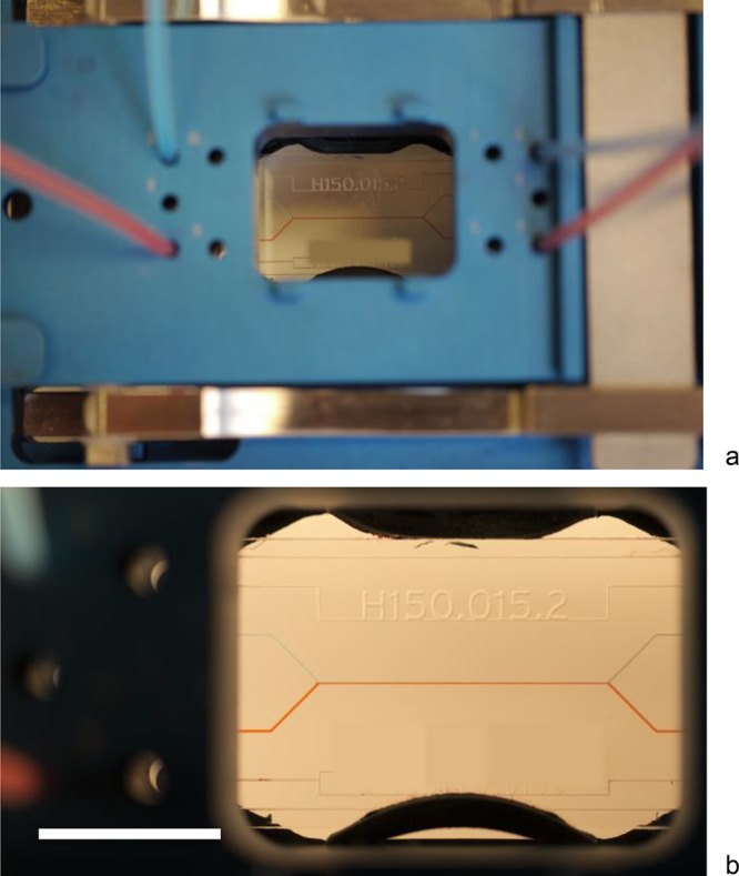
(a) Laminar flow in the H-reactor, observable macroscopically in the tubing (see also Figure 1b) and (b) with low magnification on the chip. Tubings on the left are used as inlets, with a flow rate of about 200 μL/min. The bar is 10 mm. The H-reactor is produced from borosilicate glass, using negative dry film resist and powder blasting, and has a channel width of 150–200 μm and channel depth of 150 μm.
Efficient Micromixing
Micromixing can help overcome the limitations of laminar flow. A demonstration of dye mixing can be performed with a high-efficiency split-and-recombine micromixer chip (Figure 3). Acid–base reactions using indicators like phenolphthalein or bromothymol can be applied. When the same experiment is performed in an H-reactor (see Figure 2), the difference in mixing properties and the role of diffusion can be illustrated. Using the micromixer chip, titration experiments are possible with very small quantities of fluid. For this, the ratio of pump speeds is used to determine the volume required in the titration. The pump speed of one syringe pump is kept constant, for example, at 200 μL/min. For the other pump the speed is increased in steps (e.g., 50 μL/min), starting from 10 μL/min, for example. After each speed change, several seconds to minutes later, 20–100 μL of the reaction product is collected for colorimetric inspection or addition of an indicator. The wait time required depends on the inner dimensions of the reaction channel and flow speeds. The whole procedure may be performed several times and in very small steps, such as 5 μL/min, around the equilibrium. The speed readout of the pumps at equilibrium is used to calculate the concentrations. Prior calibration of the pumps is required for reliable calculations. In this way we titrated concentration of sodium thiosulfate with a iodine solution, using starch as an indicator. Back-titration can also be done using a solution of sodium thiosulfate and iodine to titrate the concentration of ascorbic acid (vitamin C) with starch as an indicator.
Figure 3.
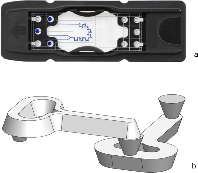
Mixer chip: (a) Layout of the mounted teardrop mixer chip (45 mm long, 15 mm wide). (b) Enlarged view of the teardrop mixing element. Channel width is 150–200 μm, and the channel depth is 150 μm. The mixer chip is produced from borosilicate glass, using negative dry film resist and powder blasting.
Other ways to mix fluids on a chip are discussed in the lesson materials, which explain the behavior of fluids using Reynolds number theory. Students are encouraged to design and fabricate their own chips and test various methods for mixing fluids on a chip. This approach is discussed in the section entitled Design Your Own Fluidic Device.
Droplet Generation
For our educational setting, we developed a focused flow droplet generator chip (Figure 4). The principle of creating microdroplets is demonstrated by creating an emulsion of oil droplets with water as the continuous phase. This chip is also suitable for producing uniform microbubbles, if pressurized gas (air, nitrogen) is introduced instead of oil.20 The required fluidic pressure is low, and it is relatively easy to find the correct settings for proper droplet formation. Students can experimentally find the relationship between fluid velocities, the formation of droplets, and the droplet size. By default, the glass channel is hydrophilic and facilitates the formation of oil-in-water droplets. Examples of applications for droplets discussed in the lesson series are vaporizers for medicine intake and the use of water-in-oil droplets for single cell analysis.21,22
Figure 4.
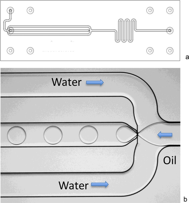
Droplet chip: (a) Layout of the focused flow droplet generator (45 mm long, 15 mm wide), with channel width 500 μm, channel depth 100 μm, nozzle width 160 μm, and nozzle depth 60 μm. (b) Formation of oil droplets in water, which is the experiment being performed by learners using the chip in Figure 1. The chip is produced from borosilicate glass, using positive resist and a wet etching (HF) technique.
Trapping and Counting of Beads
A custom-made chip was developed to demonstrate phenomena based on the use of electrodes and electronic readout with lab-on-a-chip devices. The TCB (trapping and counting of beads) chip (Figure 5) is used in combination with a lock-in amplifier developed in-house. Using the chip, students can measure conductivity, used as a measure of concentration of ions or (in specific cases) pH. They can also count and sort micrometer-sized beads using impedance spectroscopy17 and dielectrophoretic (DEP) sorting.23 Microbeads are favored over biological materials for health safety reasons. Chips are also less likely to become contaminated when using microbeads.
Figure 5.
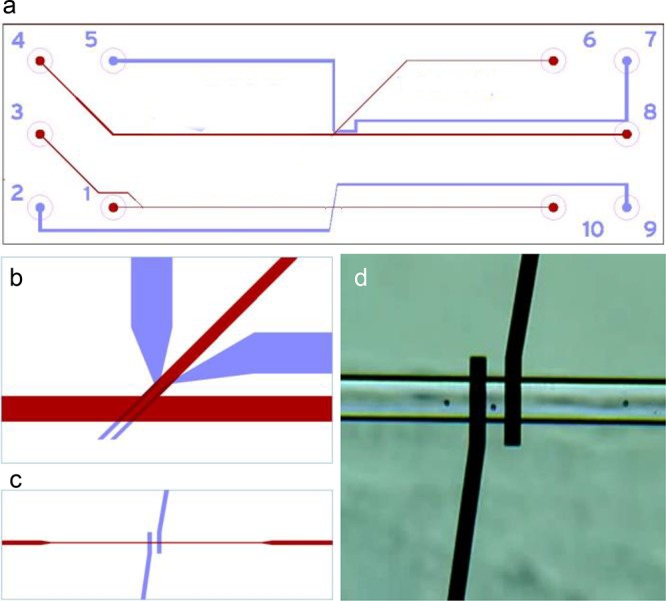
TCB chip for trapping and counting of beads: (a) Layout of the TCB chip (45 mm long, 15 mm wide). Channels (25 μm deep) are shown in red, with inlets labeled 1 (channel 70 μm wide; near the electrodes 54 μm wide), 3 (channel 70 μm wide), 4 (channel 150 μm wide), outlets labeled 6 (branch 70 μm wide), 8, 10; electrode paths (made of Pt, placed in etched and TiO coated paths) are shown in blue, with connections labeled 2, 5, 7, 9. (b) Layout of the channels and electrodes used for trapping beads or cells (electrode tips 15 μm wide). (c) Tips of the sensing electrodes (tips 25 μm wide) at the bottom of the channel (54 μm wide, as described by Segerink et al.17). (d) Microscopic view of 6 μm beads passing through the channel depicted in part c. The chip is made from borosilicate glass, using positive resist and a wet etching (HF) technique.
Experiments with the TCB chip are complicated to monitor in the classroom, and until now have been performed in the university’s outreach laboratory with expert help. Visual control over the phenomena on the chip is difficult without the help of inverted microscopy or a high-speed video camera. Therefore, the experiments are carried out with well-defined mixtures of beads or microbubbles, and easy-to-use software for the lock-in amplifier.
Design Your Own Fluidic Device
As an introductory practical that bridges the gap between the visible phenomena and microfluidics, students can make a macroscopic fluidic device themselves by using three layers of standard office lamination foil (80 μm thickness) (Figure 6). Using a standard office hole punch, holes are made in the top and middle layers, for input and output of fluids (Figure 6b). A channel pattern can be cut out in the middle layer with a fine pair of scissors, with a channel width of 0.5–2 mm. The third layer is the untreated bottom layer (Figure 6 c). The foil chip is hot-laminated by a standard lamination machine. The production of a functional fluidic device takes 15–30 min. The chip is tested with dye-solutions, but mild acidic or basic conditions and mild organic solvents and oils can also be used. For demonstration of laminar flow, diluted ink (for inkjet cartridges or fountain pens) or food coloring dyes can be used. After application of a small droplet of fluid, the dye fills the chip by capillary force and is transported by using a wicking pump made of a piece of tissue paper at the exit hole (Figure 6a). This design is excellent for demonstrating low-speed laminar flow using contrasting colors. No microscope is needed to observe this phenomenon. The freedom of design and rapid production time make this procedure with lamination foil an excellent choice for rapid prototyping purposes.24 Electrodes can be introduced by inserting thin pieces of aluminum or copper foil or wire into channels or extra punched hole(s) or between the lamination foil layers. It is also possible to build in filters fabricated from punched-out filter paper. These can help with removing debris or keeping living cells inside the chip, while transporting fluids. Students, as well as technicians and teachers, like creating fluidic devices themselves. The design and assembly process helps them to gain a basic understanding of how lab-on-a-chip devices are designed using layers and carved or etched channels. See the Supporting Information for details.
Figure 6.
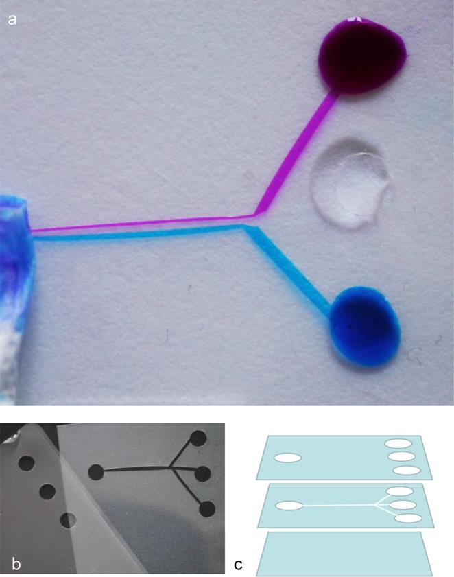
Fabrication of demonstration chips from commercial hot-lamination foil (about 80 μm thickness), using a standard office punch (6 mm punch diameter), fine scissors, and hot-lamination machine. (a) The finished chip, showing laminar flow using diluted printer inks (1:10) and water. The fluids are transported by capillary force, and propagated using tissue paper at the outlet. Channel width is about 1.5 mm. Chip outer dimensions: 50 × 60 mm. (b) Top layer (holes only, left) and middle layer (holes and channels, right). The bottom layer is untreated. (c) Schematic of the chip layers.
A second possible self-assembly method involves the production of small-scale chips out of laser-cut lamination foil fabricated using a commercial Trotec Speedy 300 laser cutter (typically at 500 dpi, 10.000 Hz, and 100 μm beam width, with a variety of power and speed settings). Designs were made using vector drawing software (Adobe Illustrator or Corel Draw). Best results were obtained using Leitz 125 μm lamination foil (Acco brands) or GBC High Speed 80 μm lamination foil (Acco brands); see Figure 7 for details. Each chip is assembled from one sheet of foil that is folded, fixed between office paper, and hot-laminated using a standard office lamination machine (Figure 7b). This type of self-produced chip can be tested as-is, or placed in the lab-on-a-chip holder, which allows the flow characteristics of the design to be checked. The adhesion of the foil layers is not perfectly strong, limiting the pressure that can be applied. Laser-cut foil chips were made in a 15 × 45 mm size, which fit the holder from the lab-on-a-chip practical kit, but also in a larger 50 × 50 mm size. This can be used as a prefabricated design, ready for assembly (see Figure 7), or in a semi-pre-fabricated way, to let students cut channels in the chip.
Figure 7.
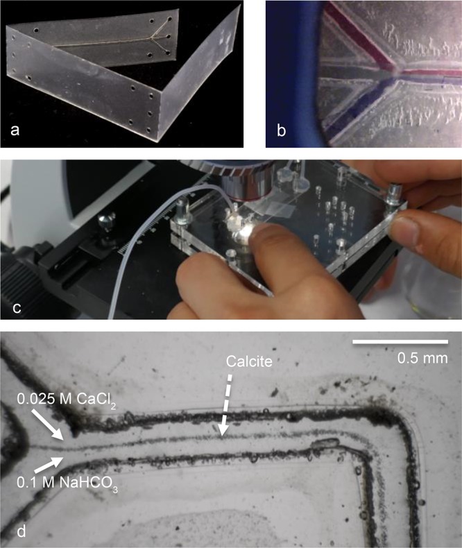
Laser-cut demonstration chips, which can be modified or redesigned by learners. (a) Laser-cut foil chip, made from 80 mm GBC High Speed laminator foil. The chips produced (outer dimensions 45 mm long, 15 mm wide, and 0.24 mm thick) are fitted on top of a 1 mm thick support plate, in the mount of the lab-on-a-chip holder. (b) The first prototype chip, showing trilaminar flow, in the chip holder. (c) A laser-cut Y reactor chip, mounted in the acrylic glass (PMMA) holder, connected with silicone ferrules. In this experiment the formation of calcite precipitate is studied, as described by Chia et al.5 (d) Calcite precipitate visible in the first part of a laser-cut serpentine mixer channel (width 100 μm, produced from 125 μm thick Leitz foil), from 0.025 M CaCl2 and 0.1 M NaHCO3 solution with syringe pumps at a flow speed of 45 μL/min. All details of the design of the foil chips and the PMMA holder are described in the Supporting Information.
A series of types of chip have been produced this way, including the H-reactor (2 in, 2 out), trilaminar flow reactor (3 in, 1 out), and various long channel serpentine reactors. The first results from the development of a simple chip holder (produced from 6 mm cast acrylic glass (PMMA)) for these student-fabricated lab-on-a-chip devices are promising. The chip holder can also be used with glass chips, but handling is less easy for this compared to the standard chip holder.
The use of standard vector drawing software allows students to (re)design a chip. If laser-cutting facilities are present, the students’ design can be produced and tested. Details related to the production of laminar foil chip devices can be found in the Supporting Information for this article.
Educational Scenario
The series of practicals was developed to be used in combination with theoretical explanations and practical instructions. Since 2012, high schools all over The Netherlands have implemented the lesson series, typically following a scenario that includes the experiments described above, which relate to various learning objectives; see Table 3. In the Supporting Information for this article, a set of exercises is presented, illustrating the concepts discussed in the lesson series.
Table 3. Example of an Educational Scenario for a Lab-on-a-Chip Lesson Series.
| Scenario Step | Activities | Goals |
|---|---|---|
| 1. Introduction | Lab-on-a-chip (LoC) applications are discussed. Students explore the layout of a typical glass LoC, the lithium chip,18 using a microscope. | Intro to microfluidics and LoC devices. |
| 2. Small LoC design | Students build and test an H-reactor with laminar foil (Figure 6). | Intro to production techniques and microfluidics concepts (e.g., capillary force, laminar flow). |
| 3. LoC experiment | Students use the H-reactor glass chip, holder, syringes, and pump to build and perform an LoC experiment (Figure 2). | Experimental skills. Microfluidics concepts (e.g., capillary force, laminar flow, diffusion). |
| 4. Advanced LoC experiments | Students use the micromixer (Figure 3) or droplet chip (Figure 4) for LoC experiments. | Experimental skills. Microfluidics concepts (e.g., Reynolds number, mixing, diffusion, hydrophilic hydrophobic interaction, droplet stability, volume-surface ratio). |
| 5. LoC project | Small group projects using the TCB chip (Figure 5), prefab laser-cut LoC device (Figure 7), or their own LoC design/prototype. | Application of microfluidics concepts. Design and engineering skills. |
Educational Outcomes and Appreciation
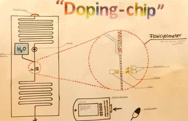
Implementation at schools shows that secondary school students can learn about microfluidics concepts with these practicals. Analyzing student test results (n = 70), we found an average score of 77% (SD = 18%) when students were asked to describe elements of a given lab-on-a-chip schematic. On the more complex question to draw a new lab-on-a-chip for a Food Safety Authority, the average score was 82% (SD = 27%). Fully correct implementation of the requirements of the chip design was achieved by 24 students. Other students made one or more mistakes, with mixing (24), logical layout and design issues (24), or omission of a detection method (5) (see Supporting Information for more details). In their small group projects, students showed that they are able to think of new lab-on-a-chip solutions for design problems (Figure 8).
Figure 8.
Student poster presenting the idea for doping detection by red blood cell counting in blood, one of the outcomes of a lab-on-a-chip project conducted at secondary schools (reproduced with permission).
When asked what they had learned most, students responded that the practicals helped them better understand the working of a lab-on-a-chip. Designing and building a chip themselves taught them more about lab-on-a-chip components and how chips are designed. Teachers and technicians report that students highly appreciate the lesson series. As the topic is new to many teachers they report that a first run can be a challenge. Careful preparation and extending the repertoire in consecutive years is a strategy applied by many. One teacher reports that the design your own chip activity (LoC project) allows for a lot of creativity, whereas some students have difficulties thinking “out-of-the-box”.
Implementation Issues
Lab-on-a-chip design solutions often relate to real-life health issues, such as the measurement of lithium ion levels in blood or the liveliness of sperm cells.17,18,25 It is clear that investigation of these issues cannot be directly transferred into classrooms. Microscopic viewing and drawing of real lab-on-a-chip devices, such as the lithium chip,18 give students an idea of their complexity. Safe fluids need to be used for application, and biological elements are replaced by polystyrene beads of different sizes.
The microscale events in lab-on-a-chip devices become more interesting if they can be viewed directly. Lab-on-a-chip devices made of glass facilitate observation using microscopes. The educational chip holder’s design allows the use of standard school microscopes or stereomicroscopes. The holder can be placed upside-down to allow the use of a webcam or USB microscope for projection on a screen. This enables these practicals to be used for demonstration purposes as well.
Costs for schools should be limited, both in terms of investment and usage. As only very small volumes of fluids are used, costs of chemicals are limited, and the environmental impact of practicals is reduced dramatically. A complete set of the practicals we present requires an investment of about €4500 (excluding VAT), with the exact price depending on the choice of fluidic chips and supplier. One set can be shared by up to 5 schools for many years, reducing the costs per school. Low-cost equipment that can be used with larger groups of students will facilitate wider implementation of microfluidics lessons in high schools.
For this reason, a simple acrylic glass (PMMA) chip holder was developed and tested at different schools. Students were able to perform a variety of experiments (on laminar flow and mixing and calcite precipitation, see Figure 7) using small and large self-assembled laser-cut foil chips. This design may be used as a low-cost introduction to the basics of microfluidics.
After initial training, teachers and technicians are supported during the lesson series if issues are experienced using the practical equipment. Teachers are supported using an online forum, via a teacher manual and via response to their feedback after finishing the lesson series. This is helpful for both professional development of the teachers and continuous improvements in the lesson series.
In the Supporting Information the components of the practical kit, details, and possible alternatives for chips and other components are listed. A troubleshooting section is also provided. In our case, schools can borrow take-away sets of practical setups that can be used for several weeks to limit costs. Schools can also decide to stick to low-cost self-assembly laminar foil chips.
Discussion and Conclusions
Lab-on-a-chip devices can be handled by secondary and undergraduate students, giving them a window into interdisciplinary frontier science projects in which they themselves might one day be involved. The lab-on-a-chip lesson series described allows the design and use of new chip devices. The practicals can be used in combination with the lesson materials or separately. Students are encouraged to build and use the lab-on-a-chip kit without technical help, and they manage to do so. The opportunity to create simple, but functional, lab-on-a-chip devices themselves stimulates students’ creativity and generates ideas for solving serious problems.
A number of publications have addressed ways to allow graduate or undergraduate students to experience lab-on-a-chip technology.26,27 These methods generally use PDMS casting, which may be time-consuming and requires higher-level teacher skills and laboratory equipment that is not always well-suited for use in high school classrooms. The practicals we present range from very cheap self-assembly systems to nearly professional measurement chips, and they can all be carried out in a standard classroom or undergraduate laboratory.
Technicians and scientists working in this field need much creativity and craftsmanship to further develop lab-on-a-chip solutions. The more advanced creation of lab-on-a-chip devices designed and fabricated by students themselves, using 3D printing of molds or new laser-cut lamination sheets, is underway. Furthermore, we hope to connect high school students with university research projects, as an additional, new way to challenge these learners.
Acknowledgments
This project was rolled out after Albert van den Berg took the initiative to make lab-on-a-chip technology available for secondary school students, thus reinvesting part of his Spinoza Award 2009. A national Dutch Physics and Chemistry grant was used to develop the TCB chip for this project. Much of the work was performed by a Teacher Development Team. We thank all of the teachers, students, scientists, and engineers who contributed to the design, production, and testing of course materials and practicals. Course materials can be found at http://www.labochip.org.
Supporting Information Available
The Supporting Information is available on the ACS Publications website at DOI: 10.1021/acs.jchemed.7b00506.
Components of the lab-on-a-chip practical kit, including information on suppliers and alternative equipment, issues, solutions, and troubleshooting section; designs and procedures for using laser-cutting for production of LoC and the acrylic chip holder; instructions for students to produce LoC from lamination foil and prefab laser-cut lamination foil; and assessment in the lesson series, samples of test questions and outcomes of student projects (PDF, DOCX)
The authors declare no competing financial interest.
Supplementary Material
References
- Fintschenko Y. Education: a modular approach to microfluidics in the teaching laboratory. Lab Chip 2011, 11, 3394–3400. 10.1039/c1lc90069b. [DOI] [PubMed] [Google Scholar]
- Bridle H.; Morton J.; Cameron P.; Desmulliez M. P. Y.; Kersaudy- Kerhoas M. Design of problem-based learning activities in the field of microfluidics for 12- to 13-year-old participants—Small Plumbing!: empowering the next generation of microfluidic engineers. Microfluid. Nanofluid. 2016, 20, 103. 10.1007/s10404-016-1770-x. [DOI] [Google Scholar]
- Hemling M.; Crooks J. A.; Oliver P. M.; Brenner K.; Gilbertson J.; Lisensky G. C.; Weibel D. B. Microfluidics for high school chemistry students. J. Chem. Educ. 2014, 91, 112–115. 10.1021/ed4003018. [DOI] [PMC free article] [PubMed] [Google Scholar]
- Piunno P. A. E.; Zetina A.; Chu N.; Tavares A. J.; Noor M. O.; Petryayeva E.; Uddayasankar U.; Veglio A. A comprehensive microfluidics device construction and characterization module for the advanced undergraduate analytical chemistry laboratory. J. Chem. Educ. 2014, 91, 902–907. 10.1021/ed400728a. [DOI] [Google Scholar]
- Chia M. C.; Sweeney C. M.; Odom T. W. Chemistry in microfluidic channels. J. Chem. Educ. 2011, 88, 461–464. 10.1021/ed1008624. [DOI] [Google Scholar]
- Feng Z. V.; Edelman K. R.; Swanson B. P. Student-fabricated microfluidic devices as flow reactors for organic and inorganic synthesis. J. Chem. Educ. 2015, 92, 723–727. 10.1021/ed5005307. [DOI] [Google Scholar]
- Greener J.; Tumarkin E.; Debono M.; Dicks A. P.; Kumacheva E. Education: a microfluidic platform for university-level analytical chemistry laboratories. Lab Chip 2012, 12, 696–701. 10.1039/c2lc20951a. [DOI] [PubMed] [Google Scholar]
- Moraes C.; Wyss K.; Brisson E.; Keith B. A.; Sun Y.; Simmons C. A. An undergraduate lab (on-a-chip): probing single cell mechanics on a microfluidic platform. Cell. Mol. Bioeng. 2010, 3, 319–330. 10.1007/s12195-010-0124-0. [DOI] [Google Scholar]
- Teerasong S.; McClain R. L. A student-made microfluidic device for electrophoretic separation of food dyes. J. Chem. Educ. 2011, 88, 465–467. 10.1021/ed100717m. [DOI] [Google Scholar]
- Yuen P. K.; Goral V. N. Low-cost rapid prototyping of whole-glass microfluidic devices. J. Chem. Educ. 2012, 89, 1288–1292. 10.1021/ed3000292. [DOI] [Google Scholar]
- Esfahani M. M. N.; Tarn M. D.; Choudhury T. A.; Hewitt L. C.; Mayo A. J.; Rubin A.; Waller M. R.; Christensen M. G.; Dawson A.; Pamme N. Lab-on-a-chip workshop activities for secondary school students Lab-on-a-chip workshop activities for secondary school students. Biomicrofluidics 2016, 10, 011301. 10.1063/1.4940884. [DOI] [PMC free article] [PubMed] [Google Scholar]
- Davis T. A.; Athey S. L.; Vandevender M. L. L. C. C.; Kolanko C. C. E.; Shao S.; Ellington M. C. G.; Dicks J. K.; Carver J. S.; Holland L. A.; Crihfield C. L. Electrolysis of water in the secondary school science laboratory with inexpensive microfluidics. J. Chem. Educ. 2015, 92, 116–119. 10.1021/ed400757m. [DOI] [Google Scholar]
- Perez-Castillejos R.; Shrirao A. B.; Raman A.; Ryll E.; Disame A.; Talasan H.. Portable, $5 microfluidics laboratory for education and outreach. In Proceedings IBER Sensors 2012, 7 ( (4), ). http://www.inaoep.mx/revista_electronica/volumen/?idnumero=d645920e395fedad7bbbed0eca3fe2e0 (accessed Nov 2017). [Google Scholar]
- Rhee M.; Burns M. A. Microfluidic assembly blocks. Lab Chip 2008, 8, 1365–1373. 10.1039/b805137b. [DOI] [PubMed] [Google Scholar]
- Giri B.; Peesara R. R.; Yanagisawa N.; Dutta D. Undergraduate laboratory module for implementing ELISA on the high performance microfluidic platform. J. Chem. Educ. 2015, 92, 728–732. 10.1021/ed4009107. [DOI] [PMC free article] [PubMed] [Google Scholar]
- Michels B. I.; Eijkelhof H. M. C.; den Braber N.. NLT: A STEM Course for Upper Secondary. RME Conference, Boulder 2013. https://prezi.com/m8jkh3s0qnhv/nlt-a-stem-course-for-upper-secondary/?utm_campaign=share&utm_medium=copy (accessed Oct 2017). [Google Scholar]
- Segerink L. I.; Sprenkels A. J.; Ter Braak P. M.; Vermes I.; Van den Berg A. On-chip determination of spermatozoa concentration using electrical impedance measurements. Lab Chip 2010, 10, 1018–1024. 10.1039/b923970g. [DOI] [PubMed] [Google Scholar]
- Floris A.; Staal S.; Lenk S.; Staijen E.; Kohlheyer D.; Eijkel J.; Van den Berg A. A prefilled, ready-to-use electrophoresis based lab-on-a-chip device for monitoring lithium in blood. Lab Chip 2010, 10, 1799–1806. 10.1039/c003899g. [DOI] [PubMed] [Google Scholar]
- Van den Brink F. T. G.; Büter L.; Odijk M.; Olthuis W.; Karst U.; Van den Berg A. Mass spectrometric detection of short-lived drug metabolites generated in an electrochemical microfluidic chip. Anal. Chem. 2015, 87, 1527–1535. 10.1021/ac503384e. [DOI] [PubMed] [Google Scholar]
- Van Hoeve W.; Dollet B.; Versluis M. W.; Lohse D. Microbubble formation and pinch-off scaling exponent in flow-focusing devices. Phys. Fluids 2011, 23, 092001. 10.1063/1.3631323. [DOI] [Google Scholar]
- Kemna E. W. M.; Schoeman R. M.; Wolbers F.; Vermes I.; Weitz D. A.; Van den Berg A. (2012) High-yield cell ordering and deterministic cell-in-droplet encapsulation using Dean flow in a curved microchannel. Lab Chip 2012, 12, 2881–2887. 10.1039/c2lc00013j. [DOI] [PubMed] [Google Scholar]
- Schoeman R. M.; Kemna E. W. M.; Wolbers F.; Van den Berg A. High-throughput deterministic single-cell encapsulation and droplet pairing, fusion, and shrinkage in a single microfluidic device. Electrophoresis 2014, 35, 385–392. 10.1002/elps.201300179. [DOI] [PubMed] [Google Scholar]
- Gossett D. R.; Weaver W. M.; Mach A. J.; Hur S. C.; Tse H. T. K.; Lee W.; Amini H.; Di Carlo D. Label-free cell separation and sorting in microfluidic systems. Anal. Bioanal. Chem. 2010, 397, 3249–3267. 10.1007/s00216-010-3721-9. [DOI] [PMC free article] [PubMed] [Google Scholar]
- Focke M.; Kosse D.; Müller C.; Reinecke H.; Zengerle R.; von Stetten F. Lab-on-a-Foil: microfluidics on thin and flexible films. Lab Chip 2010, 10, 1365–1386. 10.1039/c001195a. [DOI] [PubMed] [Google Scholar]
- Ávila M.; Floris A.; Staal S.; Ríos Á.; Eijkel J.; van den Berg A. Point of care creatinine measurement for diagnosis of renal disease using a disposable microchip. Electrophoresis 2013, 34, 2956–2961. 10.1002/elps.201300255. [DOI] [PubMed] [Google Scholar]
- Piunno P. A. E.; Boyd C.; Barzda V.; Gradinaru C. C.; Krull U. J.; Stefanovic S.; Stewart B. The advanced interdisciplinary research laboratory: A student team approach to the fourth-year research thesis project experience. J. Chem. Educ. 2014, 91, 655–661. 10.1021/ed4005968. [DOI] [Google Scholar]
- Liu Y. BioMEMS and lab-on-a-chip course education at West Virginia University. Biosensors 2011, 1, 4–12. 10.3390/bios1010004. [DOI] [PMC free article] [PubMed] [Google Scholar]
Associated Data
This section collects any data citations, data availability statements, or supplementary materials included in this article.


