Abstract
Both p-type and n-type MoTe2 transistors are needed to fabricate complementary electronic and optoelectronic devices. In this study, we fabricate air-stable p-type multi-layered MoTe2 transistors using Au as electrode and achieve the conversion of p-type transistor to n-type by annealing it in vacuum. Temperature-dependent in situ measurements assisted by the results given by first-principle simulations indicate that n-type conductance is an intrinsic property, which is attributed to tellurium vacancies in MoTe2, while the device in air experiences a charge transfer which is caused by oxygen/water redox couple and is converted to air-stable p-type transistor. Based on p-type and n-type multi-layered MoTe2 transistors, we demonstrate a complementary inverter with gain values as high as 9 at VDD = 5 V.
Electronic supplementary material
The online version of this article (10.1186/s11671-018-2721-0) contains supplementary material, which is available to authorized users.
Keywords: MoTe2, P-type, N-type, Absorbates, Vacancies
Background
Graphene and similar two-dimensional (2D) materials exist in bulk form as stacks of strongly bonded layers with weak interlayer attraction, allowing itself to be exfoliated into atomically thin layers, which have opened up new possibilities for the exploration of 2D physics as well as that of new material applications [1–9]. Of them, semiconductor transition metal dichalcogenides (TMDs) exhibit sizeable bandgaps [2, 3, 10, 11]. In addition, these 2D TMD flakes are flexible and free of dangling bonds between adjacent layers [12, 13]. These unique properties make TMDs promising candidates to construct electronic and optoelectronic devices [2–4, 14], such as next-generation field-effect transistor (FET) at sub 10 nm [15], inverter [16–22], and on-chip light-emitting diode (LED) [23–25] and Van der Waals heterostructure devices [4, 5, 26–28].
2H-type molybdenum ditelluride (2H-MoTe2) is one of the typical 2D TMDs, which has an indirect bandgap of 0.83 eV in bulk form [29] and a direct bandgap of 1.1 eV when it is thinned to a monolayer [30]. 2H-MoTe2 has been explored for applications in spintronics [31], FET [32–34], photodetector [35–38], and solar cell [39]. Like most 2D materials, multi-layered 2H-MoTe2 has very high surface-to-volume ratio, making it sensitive to various influences in the surrounding environment. Thus, it is difficult to obtain its intrinsic properties. The surface and interface of 2D materials and related devices have always been research hotspots in order to achieve higher performance. Here, we fabricate a multi-layered 2H-MoTe2 transistor, whose source and drain electrode layers are fabricated, and then, a multi-layered MoTe2 sample is transferred to bridge the source and drain electrodes as a transistor channel. The whole MoTe2 sample is exposed in air, including the channel and contact part, which is advantageous to investigating the influence of absorbates on charge transport properties of multi-layered MoTe2 transistor. Measurements of vacuum- and temperature-dependent charge transport are conducted. The experimental data show that multi-layered MoTe2 transistor is an n-type in terms of intrinsic conductance. However, the device exposed in air can be doped by absorbates and converted to air-stable p-type transistor. We infer that the intrinsic n-type conductance of multi-layered MoTe2 transistor is attributed to tellurium (Te) vacancies, which is confirmed by density functional theory (DFT) calculations. The conversion to p-type conductance in air can be explained by the fact that oxygen and water absorbed in air can induce electron transfer from MoTe2 to oxygen/water redox couple, which converts n-type multi-layered MoTe2 transistor to p-type. Finally, based on the n-type and p-type multi-layered MoTe2 transistors, we demonstrate a complementary inverter, which shows symmetric input/output behavior and gain values of 9 at VDD = 5 V.
Results and Discussion
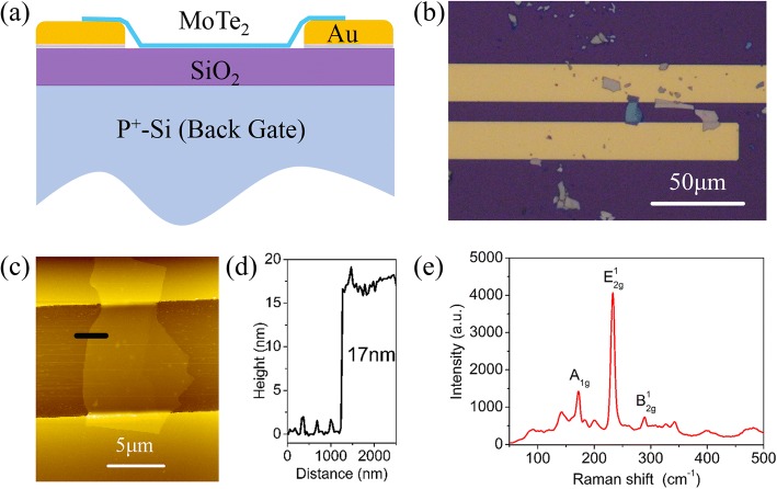
Different from the previously reported multi-layered MoTe2 transistor, our device diagram is shown in Fig. 1a. We first fabricate source-drain (SD) electrodes composed of Cr/Au film on SiO2/p+-Si substrate. Then, one of the multi-layered MoTe2 samples prepared on another SiO2/ p+-Si substrate is transferred to bridge the source-drain electrodes as transistor channel. The MoTe2 sample made by this method is clean and free of polymer contamination in device fabrication. In addition, the whole MoTe2 sample is exposed in air, including the channel and contact part, making it more convenient to remove absorbates and obtain intrinsic conductance of multi-layered MoTe2 transistor. An optical image of a fabricated multi-layered MoTe2 transistor is shown in Fig. 1b, with a channel length of 10 μm. The MoTe2 channel is characterized by atomic force microscopy (AFM) (see Fig. 1c). Height profile (see Fig. 1d) obtained from the mark in AFM image indicates that the thickness of MoTe2 sample is about 17 nm (composed of 24 monolayer MoTe2) [40]. The characteristic Raman-active modes of A1g (172 cm−1), E12g (233 cm−1), and B12g (289 cm−1) are clearly observed as shown in Fig. 1e, indicating the good quality of 2H-MoTe2 after the transfer process [41].
Fig. 1.
Multi-layered MoTe2 transistor and its properties. a Illustration of MoTe2 transistor diagram. b Optical image of one of the fabricated transistors composed of multi-layered MoTe2 channel and SD Cr/Au electrodes. c AFM image of the transistor channel in b. d Height profile of the multi-layered MoTe2. e Raman spectrum of the multi-layered MoTe2 in the transistor channel
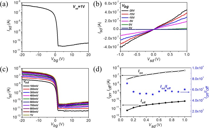
The fabricated back-gated multi-layered MoTe2 transistors are measured using Agilent B1500A semiconductor analyzer in Lakeshore probe station, which can be pumped to a base pressure of 1 × 10⁻⁵ mbar and realize 9~350 K temperature adjustment. Figure 2 shows the electric properties of a multi-layered MoTe2 transistor in air at room temperature (RT). The transfer characteristics at source-drain voltage Vsd = 1 V in Fig. 2a show that the transistor is in on-state at negative gating voltage and in off-state at positive gating voltage. The transform voltage from on-state to off-state is nearly zero, which is a typical p-type transistor characteristic. Replicate measurements show the same electric gating characteristics (see Additional file 1: Figure S1). Four other multi-layered MoTe2 transistors also demonstrate similar p-type electric gating characteristics as shown in Additional file 1: Figure S2. We also prepare other devices with thicknesses of 5 nm, 38 nm, and 85 nm as shown in Additional file 1: Figure S3. When the MoTe2 thicknesses are 5 nm and 38 nm, both the prepared devices show p-type conductance but with small on-current compared with the device in Fig. 2 and Additional file 1: Figure S2. As the thickness increases to 85 nm, the gating effect disappears as shown in Additional file 1: Figure S3 (l). These data show that p-type conductance is universal in air for multi-layered MoTe2 transistor. From transfer characteristics in Fig. 2a, we can obtain the on-off ratio, subthreshold swing (SS), and field-effect mobility (μ), which are 6 × 10³, 350 mV/dec, and 8 cm2/V·s, respectively.
Fig. 2.
Electric properties of multi-layered MoTe2 transistor in air at RT. a Transfer characteristics of MoTe2 transistor at Vsd = 1 V in air. b Output characteristics of MoTe2 transistor at Vbg = − 20 V, − 15 V, − 10 V, − 5 V, 0 V, and 5 V. c Transfer characteristics of MoTe2 transistor at different Vsd. d On-current, off-current, and on-off current ratio as function of Vsd
Figure 2b shows the output characteristics of multi-layered MoTe2 transistor at back-gate voltage Vbg = − 20 V, − 15 V, − 10 V, − 5 V, 0 V, and 5 V. As seen, the response is essentially linear, especially at low biased voltage of Vsd, which indicates there is negligible effective Schottky barrier height (ΦSB) between Au and MoTe2 in air. The transfer characteristics at different source-drain biased voltages as shown in Fig. 2c indicate that the on-current increases linearly with biased voltage Vsd, shown in Fig. 2d, which coincides with the output characteristics. Meanwhile, the off-current increases and on-off ratio decreases as Vsd increases. This can be attributed to trap state in MoTe2 channel from absorbates and interface state. The hysteresis in transfer characteristics (see Additional file 1: Figure S4) further confirms the existence of trap state in MoTe2 transistor [42–45].
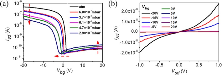
We further investigate the p-type conductance of multi-layered MoTe2 transistor at different vacuums. This is helpful to understand the influence of absorbed oxygen and water on the charge transport properties. Figure 3a shows the transfer characteristics at Vsd = 1 V as a function of vacuum (“atm” corresponds to atmosphere). The major changing tendencies are clearly indicated by red arrows, which is similar to that shown in carbon nanotube transistor [44]. First, the on-current decreases as vacuum increases, which is partially due to the shift of threshold voltage caused by absorbates but mainly due to device resistance increase as absorbates decrease, including channel and contact resistance. The nonlinear output characteristics as shown in Fig. 3b indicate the enhanced effective Schottky barrier between Au and MoTe2 in 2.9 × 10⁻⁵ mbar vacuum, which suggests that the effective Schottky barrier height is modified by absorbates in air. Second, the off-current at positive voltage gating increases with the vacuum, which means that electron conductance increases as absorbates decrease and suggests that n-type conductance is suppressed in multi-layered MoTe2 transistor by absorbates in air.
Fig. 3.
P-type electric properties of multi-layered MoTe2 transistor in vacuum. a RT transfer characteristics of a p-type MoTe2 transistor at Vsd = 1 V as a function of vacuum. b RT output characteristics of a p-type MoTe2 transistor at different Vbg in 2.9 × 10⁻⁵ mbar vacuum
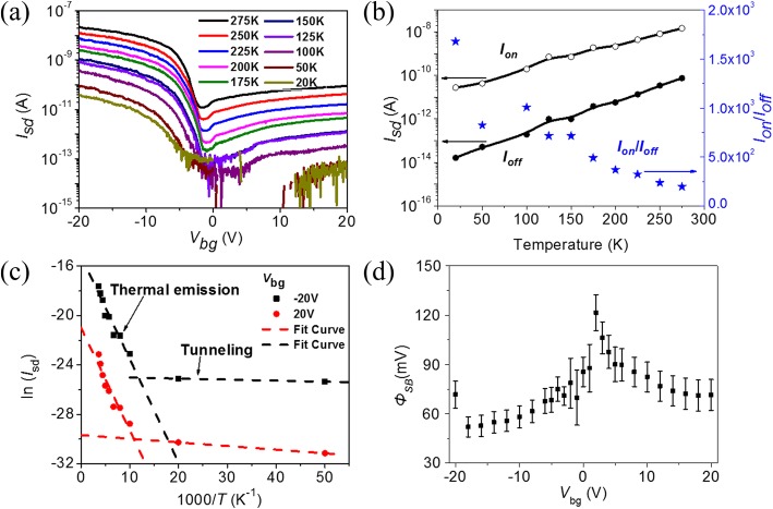
Although the on-current decreases and off-current increases after eliminating partial absorbates in vacuum, the multi-layered MoTe2 transistor still exhibits p-type conductance. Furthermore, p-type conductance maintains at low temperature as shown in Fig. 4a. This temperature-dependent electric property helps us to further elucidate the charge transport mechanism and extract the effective Schottky barrier height of p-type MoTe2 transistor. Figure 4a gives the transfer characteristics at biased voltage Vsd = 1 V as temperature varies from 20 to 275 K. Both on-current and off-current decrease as temperature decreases, and the on-off ratio increases at low temperatures as shown in Fig. 4b. Arrhenius plot of the source-drain current Isd at back-gate voltage Vsd = − 20 V and 20 V in Fig. 4c indicates the thermal emission and tunneling contribution for charge transport [46]. When temperature is higher than 100 K, a clear thermal emission region is observed in both negative and positive gating voltages, and the tunneling current dominates when temperature is below 100 K. That is why both on-current and off-current decrease as temperature decreases. Based on the thermal emission current observation and the relationship of , where k is the Boltzmann constant and T is temperature, we extract the effective Schottky barrier height ΦSB as a function of gate voltage at Vsd = 1 V, as shown in Fig. 4d. The effective Schottky barrier heights ΦSB in both on- and off-state are smaller than 120 mV.
Fig. 4.
Temperature-dependent electric properties of a p-type multi-layered MoTe2 transistor. a Transfer characteristics of MoTe2 transistor at Vsd = 1 V as a function of temperature. b On-current, off-current, and on-off current ratio as a function of temperature. c Arrhenius plot of the source-drain current as a function of temperature at Vsd = 1 V and Vbg = − 20 V and 20 V, respectively. d Maps of effective Schottky barrier heights ΦSB as a function of back-gate voltage
Vacuum and low temperature make it difficult to desorb the absorbates completely. The residual absorbates still work and alter the conductance of multi-layered MoTe2 transistor. In order to further desorb the absorbates on MoTe2 transistor, we heat the device to 350 K in vacuum and carry out in situ electric property measurements. Figure 5a shows the transfer characteristics of MoTe2 transistor as it is heated from 250 to 350 K. As seen, the electron conductance at positive gate voltage is enhanced, while hole conductance at negative gate voltage is reduced as temperature increases. At temperature T = 250 K, the device shows a typical p-type conductance. But when temperature increases to T = 350 K, the device is converted to n-type, which is in off-state at negative gate voltage and in on-state at positive gate voltage. Its on-off ratio, subthreshold swing (SS), and field-effect mobility (μ) are 3.8 × 10², 1.1 V/dec, and 2 cm2/V·s, respectively.
Fig. 5.
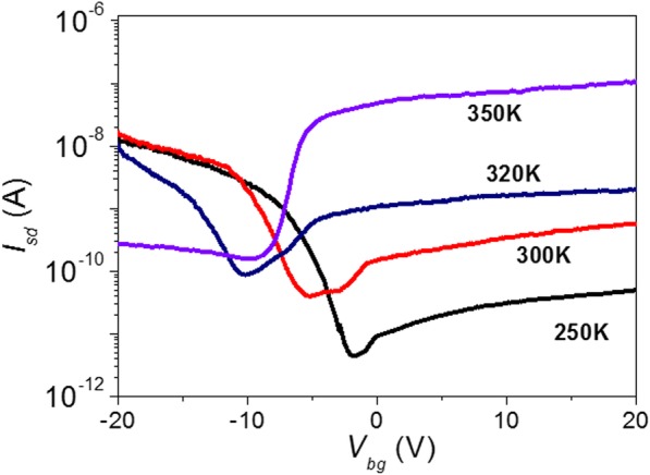
The transfer characteristics of multi-layered MoTe2 transistor as a function of temperature in vacuum
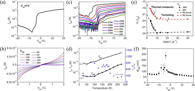
The n-type conductance of a MoTe2 transistor is stable in vacuum. The device is kept in probe station in 2 × 10⁻⁵ mbar vacuum at RT for 12 h after heating. Then, the measurements of electric properties are conducted. As shown in Fig. 6a, the transfer characteristics are still in off-state at negative gate voltage and in on-state at positive gate voltage, demonstrating typical n-type transistor properties. Similar transformations are realized in the other two samples as shown in Additional file 1: Figure S5 (a) and (b). Furthermore, we anneal two samples at 523 K using a high-temperature chemical vapor deposition system for 2 h in Ar gas at 3 mbar vacuum. They both change from p-type to n-type as shown in Additional file 1: Figure S5 (c) and (d). Figure 6b shows the output characteristics of an n-type MoTe2 transistor at different back-gate voltages, which is clearly nonlinear, especially at low biased voltage Vsd, different from that in Fig. 3b, indicating the existence of enhanced effective Schottky barrier height between MoTe2 and Au electrode after being heated to remove absorbates. Figure 6c shows the temperature-dependent transfer characteristics of n-type multi-layered MoTe2 transistor. As seen, when temperature decreases from 275 to 25 K, the on-current and off-current both decrease as shown in Fig. 6c, d. Arrhenius plot of the source-drain current Isd in Fig. 6e shows that thermal emission and tunneling current are still the main charge transport mechanism in n-type multi-layered MoTe2 transistor. The effective Schottky barrier height thus obtained is smaller than 250 meV. Considering the work function of Au (5.2 eV) and MoTe2 (4.1 eV), the effective Schottky barrier height for electron is as high as 1.1 eV in ideal condition. The difference may be from the Fermi level pinning effect in 2D materials [47].
Fig. 6.
N-type multi-layered MoTe2 transistor properties in vacuum. a RT transfer characteristics of MoTe2 transistor at Vsd = 1 V. b RT output characteristics of MoTe2 transistor at different back-gate voltage. c Transfer characteristics of MoTe2 transistor as a function of temperature. d On-current, off-current, and on-off current ratio of MoTe2 transistor as a function of temperature. e Arrhenius plot of the Isd at Vsd = 1 V and Vbg = − 20 V and 20 V, respectively. f Maps of effective Schottky barrier heights ΦSB as a function of Vbg
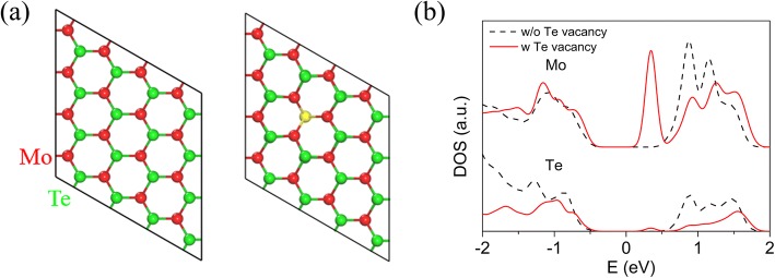
We also find that the n-type multi-layered MoTe2 transistor returns to p-type when it is exposed to air (see Additional file 1: Figure S6). Based on the above experiment data, we infer that n-type conductance is an intrinsic property for multi-layered MoTe2 transistor. N-type conductance can be attributed to Te vacancy in MoTe2 channel. It is confirmed by DFT calculation as shown in Fig. 7. Figure 7a shows the illustration of the diagram of Te vacancy in monolayer (ML) MoTe2, and Fig. 7b shows the corresponding density of states (DOS). Compared with the DOS of MoTe2 with perfect crystal structure, Te vacancy induces a defect state near the conduct band edge. Therefore, MoTe2 transistor with Te vacancy demonstrates n-type conductance.
Fig. 7.
Te vacancy in MoTe2. a 4 × 4 ML MoTe2 supercells in an ideal phase and with a Te vacancy. The vacancy site is marked in yellow. b Partial density of states (PDOS) of Mo site adjacent to Te vacancy and nearest Te site to a Te vacancy in ML MoTe2 (red solid), compared to the PDOS in an ideal ML (black dashed)
When the device is exposed to air, oxygen and water in air are absorbed on the device. It has been verified that the absorbates of oxygen and water can induce p-type doping in organic transistor and graphene-related layer material transistor [44, 48, 49]. It works by oxygen/water redox couple, in which the solved oxygen in water sets the condition for the redox reaction. This process will induce charge transfer between the oxygen/water redox couple and MoTe2. Charge transfer direction depends on the work function (or chemical potential) difference. The work function of MoTe2 is 4.1 eV, while that of oxygen/water redox couple is larger than 4.83 eV [48]. Figure 8 illustrates the energy diagram of the water/oxygen redox couple and MoTe2. Due to the energy level difference, the electrons are injected from MoTe2 to oxygen/water redox couple, resulting in hole doping of MoTe2 in air.
Fig. 8.
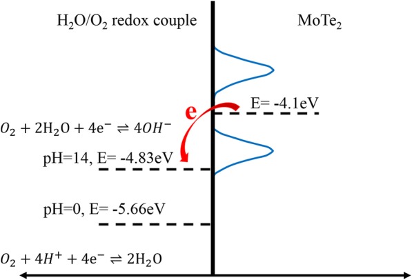
Energy diagram of the water/oxygen redox couple (left) and MoTe2 (right); the red arrow indicates the electron transfer direction
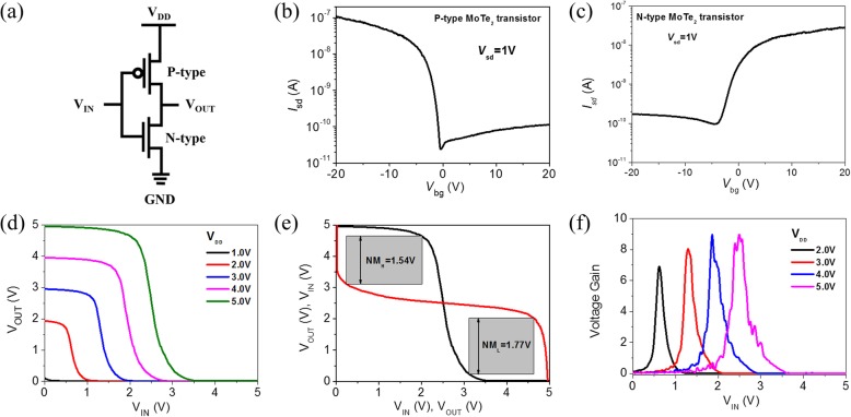
Using the p-type and n-type MoTe2 transistors, we explore the construction of a complementary inverter as illustrated in Fig. 9a. A supply voltage of VDD is applied to the source (or drain) of p-type transistors, while the source (or drain) of the n-type transistor is grounded. The inverter is measured in 8 × 10⁻⁵ mbar vacuum in probe station. Figure 9b, c shows the transfer characteristics of p-type and n-type transistors from the inverter, respectively. Figure 9d shows the voltage transfer characteristics (VTC) curves of the inverter when VDD varies in the range of 1 to 5 V. The transition voltage is located very near to VDD/2, which can be attributed to the symmetry between n- and p-type MoTe2 transistors. Figure 9e shows the VTC curves (black lines) and their mirrors (red lines) at VDD = 5 V. The shaded “eye” area represents the noise margin of the inverter. As seen, the low-level noise margin (NML) and high-level noise margin (NMH) are 1.54 V and 1.77 V, respectively, at VDD = 5 V. Figure 9f shows VIN-dependent voltage gains of the inverter at VDD = 2 V, 3 V, 4 V, and 5 V which increases with VDD and reaches 9 at VDD = 5 V.
Fig. 9.
Complementary inverter properties based on p-type and n-type multi-layered MoTe2 transistor in 8 × 10⁻⁵ mbar vacuum. a Inverter diagram composed of p-type and n-type MoTe2 transistors. Transfer characteristics of p-type (b) and n-type (c) MoTe2 transistor from the inverter. d VTC curves of the inverter for VDD values varying from 1 to 5 V. e VTC curves (black lines) and their mirrors (red lines) at VDD = 5 V. f VIN-dependent voltage gains of the inverter at VDD = 2 V, 3 V, 4 V, and 5 V
Conclusions
In summary, we have fabricated a p-type multi-layered MoTe2 transistor by transferring MoTe2 onto fabricated source-drain electrode in air. Vacuum- and temperature-dependent in situ charge transport measurements demonstrate that the usual p-type conductance of multi-layered MoTe2 transistor is not its intrinsic properties, which is caused by oxygen/water redox couple doping in air. When the MoTe2 transistor is heated in vacuum to remove absorbates, it exhibits n-type conductance, which is attributed to tellurium vacancies in MoTe2 and is its intrinsic transport property. Both p-type and n-type MoTe2 transistors show smaller effective Schottky barrier height, which is partially due to the modification by absorbates. The lowered effective Schottky barrier is beneficial to achieving a high-performance MoTe2 transistor. Based on these findings, we fabricate a complementary inverter with gain values as high as 9.
Methods/Experimental
In order to research the influence of adsorbates on charge transport properties of multi-layered MoTe2 transistor, we choose back-gated multi-layered MoTe2 transistors and the whole MoTe2 sample is exposed to the surroundings. Back-gated multi-layered MoTe2 transistors are fabricated as follows. First, source, drain, and gate electrodes are patterned on 300-nm SiO2/p+-Si substrate using standard UV photolithography techniques, followed by selective etching of 300-nm SiO2 beneath the gate electrode and E-beam evaporation of a 5-nm/100-nm Cr/Au film. Second, multi-layered MoTe2 samples are prepared on other 300-nm SiO2/p+-Si by mechanical exfoliation of millimeter-size semiconducting 2H-MoTe2 single crystals, which are grown by chemical vapor transport using TeCl4 as the transport agent in a temperature gradient of 750 to 700°C for 3 days. Finally, the prepared multi-layered MoTe2 samples are transferred onto patterned source-drain electrode using polyvinyl alcohol (PVA) as medium [50]. PVA is dissolved in H2O and rinsed with isopropyl alcohol (IPA). Device annealing is carried out in a chemical vapor deposition setup with dry pump. Multi-layered MoTe2 samples are identified by an optical microscope, and the corresponding thickness is characterized using SPA-300HV atomic force microscopy (AFM). Raman signals are collected by a LabRAM HR Raman spectrometer with 514-nm wavelength laser excitation in the backscattering configuration using a ×100 objective. The laser power measured from the objective is 2.2 mW. Electrical characterization is performed using a combination of Agilent B1500A semiconductor analyzer with Lakeshore probe station.
The DFT calculations are performed with the projector-augmented wave (PAW) pseudopotential and plane-wave basis set with a cut-off energy of 400 eV implemented in the Vienna ab initio simulation package (VASP) [51]. A vacuum space above 15 Å is chosen in order to eliminate the spurious interaction between periodic images. Enough k-point sampling of 12 × 12 × 1 and 24 × 24 × 1 are used for the structure relaxation and electronic calculations, respectively. The generalized gradient approximation (GGA) with Perew-Burke-Ernzerhof (PBE) functional is adopted [52].
Additional file
Figure S1. Transfer characteristics of replicate measurements. Figure S2. (a)-(d) show the transfer characteristics of other four multi-layered MoTe2 transistors in air, respectively. Figure S3. MoTe2 transistor with different thicknesses. (a)~(d) show the optical image, AFM image, height profile, and transfer characteristics of the device with 5-nm thickness, respectively. (e)~(h) show the optical image, AFM image, height profile, and transfer characteristics of the device with 38-nm thickness, respectively. (i)~(l) show the optical image, AFM image, height profile, and transfer characteristics of the device with 85-nm thickness, respectively. Figure S4. Hysteresis behavior of transfer characteristics of multi-layered MoTe2 transistor. Figure S5. (a)-(d) show the transfer characteristics of four multi-layered MoTe2 transistors, respectively. The black line represents the transfer characteristics of as-prepared multi-layered MoTe2 transistor in air, and the red line represents that measured from the annealed device. Figure S6. (a)-(c) show the transfer characteristics of three multi-layered MoTe2 transistors at different conditions, respectively. (DOCX 1011 kb)
Acknowledgments
Funding
This work was financially supported by the National Natural Science Foundation of China (51502337, 11574171, and 51472019) and Open Research Fund Program of the State Key Laboratory of Low-Dimensional Quantum Physics.
Availability of Data and Materials
The datasets supporting the conclusions of this article are included within the article and its supporting information.
Abbreviation
- 2D
Two-dimensional
- 2H-MoTe2
2H-type molybdenum ditelluride
- AFM
Atomic force microscopy
- DFT
Density functional theory
- DOS
Density of states
- FET
Field-effect transistor
- GGA
Generalized gradient approximation
- IPA
Isopropyl alcohol
- Isd
Source-drain current
- LED
Light-emitting diode
- NMH
High-level noise margin
- NML
Low-level noise margin
- PAW
Projector-augmented wave
- PBE
Perew-Burke-Ernzerhof
- PVA
Polyvinyl alcohol
- SD
Source-drain
- SS
Subthreshold swing
- TMDs
Transition metal dichalcogenides
- VASP
Vienna ab initio simulation package
- Vbg
Back-gate voltage
- Vsd
Source-drain voltage
- VTC
Voltage transfer characteristics
- ΦSB
Schottky barrier height
Authors’ Contributions
JL conceived the experiment. JL and LX designed the experiment, performed the measurements, and drafted the manuscript with the assistance of NG and YJ. XX fabricated the device with the assistance of QL. YW performed the DFT calculations. KZ grew 2H-MoTe2 single crystals with the assistance of YW and SZ. All authors discussed the results and approved the final manuscript.
Competing Interests
The authors declare that they have no competing interests.
Publisher’s Note
Springer Nature remains neutral with regard to jurisdictional claims in published maps and institutional affiliations.
Contributor Information
Junku Liu, Email: liujunku@qxslab.cn.
Yangyang Wang, Email: wangyangyang@qxslab.cn.
Xiaoyang Xiao, Email: xiao-xy13@mails.tsinghua.edu.cn.
Kenan Zhang, Email: zhangkenan1993@gmail.com.
Nan Guo, Email: guonan@qxslab.cn.
Yi Jia, Email: jiayi@qxslab.cn.
Shuyun Zhou, Email: syzhou@mail.tsinghua.edu.cn.
Yang Wu, Email: wuyang.thu@gmail.com.
Qunqing Li, Email: qunqli@tsinghua.edu.cn.
Lin Xiao, Email: xiaolin@qxslab.cn.
References
- 1.Novoselov KS, Jiang D, Schedin F, et al. Two-dimensional atomic crystals. Proc Natl Acad Sci U S A. 2005;102:10451–10453. doi: 10.1073/pnas.0502848102. [DOI] [PMC free article] [PubMed] [Google Scholar]
- 2.Mak KF, Shan J. Photonics and optoelectronics of 2D semiconductor transition metal dichalcogenides. Nat Photonics. 2016;10:216–226. [Google Scholar]
- 3.Wang QH, Kalantar-Zadeh K, Kis A, et al. Electronics and optoelectronics of two-dimensional transition metal dichalcogenides. Nat Nanotechnol. 2012;7:699–712. doi: 10.1038/nnano.2012.193. [DOI] [PubMed] [Google Scholar]
- 4.Liu Y, Weiss NO, Duan X, et al. Van der Waals heterostructures and devices. Nat Rev Mater. 2016;1:16042. [Google Scholar]
- 5.Geim AK, Grigorieva IV. Van der Waals heterostructures. Nature. 2013;499:419–425. doi: 10.1038/nature12385. [DOI] [PubMed] [Google Scholar]
- 6.Bhimanapati GR, Lin Z, Meunier V, et al. Recent advances in two-dimensional materials beyond graphene. ACS Nano. 2015;9:11509–11539. doi: 10.1021/acsnano.5b05556. [DOI] [PubMed] [Google Scholar]
- 7.Butler SZ, Hollen SM, Cao L, et al. Progress, challenges, and opportunities in two-dimensional materials beyond graphene. ACS Nano. 2013;7:2898–2926. doi: 10.1021/nn400280c. [DOI] [PubMed] [Google Scholar]
- 8.Novoselov KS, Mishchenko A, Carvalho A, Neto AHC. 2D materials and van der Waals heterostructures. Science. 2016;353:aac9439. doi: 10.1126/science.aac9439. [DOI] [PubMed] [Google Scholar]
- 9.Chhowalla M, Jena D, Zhang H. Two-dimensional semiconductors for transistors. Nat Rev Mater. 2016;1:16052. [Google Scholar]
- 10.Mak KF, Lee C, Hone J, et al. Atomically thin MoS2: a new direct-gap semiconductor. Phys Rev Lett. 2010;105:136805. doi: 10.1103/PhysRevLett.105.136805. [DOI] [PubMed] [Google Scholar]
- 11.Splendiani A, Sun L, Zhang Y, et al. Emerging photoluminescence in monolayer MoS2. Nano Lett. 2010;10:1271–1275. doi: 10.1021/nl903868w. [DOI] [PubMed] [Google Scholar]
- 12.Chhowalla M, Shin HS, Eda G, et al. The chemistry of two-dimensional layered transition metal dichalcogenide nanosheets. Nat Chem. 2013;5:263–275. doi: 10.1038/nchem.1589. [DOI] [PubMed] [Google Scholar]
- 13.Velusamy DB, Kim RH, Cha S, et al. Flexible transition metal dichalcogenide nanosheets for band-selective photodetection. Nat Commun. 2015;6:8063. doi: 10.1038/ncomms9063. [DOI] [PMC free article] [PubMed] [Google Scholar]
- 14.Podzorov V, Gershenson ME, Kloc C, et al. High-mobility field-effect transistors based on transition metal dichalcogenides. Appl Phys Lett. 2004;84:3301–3303. [Google Scholar]
- 15.Nourbakhsh A, Zubair A, Sajjad RN, et al. MoS2 field-effect transistor with sub-10 nm channel length. Nano Lett. 2016;16:7798–7806. doi: 10.1021/acs.nanolett.6b03999. [DOI] [PubMed] [Google Scholar]
- 16.Yu L, Zubair A, Santos EJG, et al. High-performance WSe2 complementary metal oxide semiconductor technology and integrated circuits. Nano Lett. 2015;15:4928–4934. doi: 10.1021/acs.nanolett.5b00668. [DOI] [PubMed] [Google Scholar]
- 17.Cho A-J, Park KC, Kwon J-Y. A high-performance complementary inverter based on transition metal dichalcogenide field-effect transistors. Nanoscale Res Lett. 2015;10:115. doi: 10.1186/s11671-015-0827-1. [DOI] [PMC free article] [PubMed] [Google Scholar]
- 18.Takenobu T. CMOS inverters and P-N junction diodes based on transition metal dichalcogenide monolayers. Meet Abstr MA. 2014;02:2136–2136. [Google Scholar]
- 19.Das S, Dubey M, Roelofs A. High gain, low noise, fully complementary logic inverter based on bi-layer WSe2 field effect transistors. Appl Phys Lett. 2014;105:083511. [Google Scholar]
- 20.Jeon PJ, Kim JS, Lim JY, et al. Low power consumption complementary inverters with n-MoS2 and p-WSe2 dichalcogenide nanosheets on glass for logic and light-emitting diode circuits. ACS Appl Mater Interfaces. 2015;7:22333–22340. doi: 10.1021/acsami.5b06027. [DOI] [PubMed] [Google Scholar]
- 21.Tosun M, Chuang S, Fang H, et al. High-gain inverters based on WSe2 complementary field-effect transistors. ACS Nano. 2014;8:4948–4953. doi: 10.1021/nn5009929. [DOI] [PubMed] [Google Scholar]
- 22.Lim JY, Pezeshki A, Oh S, et al. Homogeneous 2D MoTe2 p–n junctions and CMOS inverters formed by atomic-layer-deposition-induced doping. Adv Mater. 2017;29:1701798. doi: 10.1002/adma.201701798. [DOI] [PubMed] [Google Scholar]
- 23.Ross JS, Klement P, Jones AM, et al. Electrically tunable excitonic light-emitting diodes based on monolayer WSe2 p-n junctions. Nat Nanotechnol. 2014;9:268–272. doi: 10.1038/nnano.2014.26. [DOI] [PubMed] [Google Scholar]
- 24.Withers F, Del Pozo-Zamudio O, Mishchenko A, et al. Light-emitting diodes by band-structure engineering in van der Waals heterostructures. Nat Mater. 2015;14:301–306. doi: 10.1038/nmat4205. [DOI] [PubMed] [Google Scholar]
- 25.Cheng R, Li D, Zhou H, et al. Electroluminescence and photocurrent generation from atomically sharp WSe2/MoS2 heterojunction p–n diodes. Nano Lett. 2014;14:5590–5597. doi: 10.1021/nl502075n. [DOI] [PMC free article] [PubMed] [Google Scholar]
- 26.Kang J, Tongay S, Zhou J, et al. Band offsets and heterostructures of two-dimensional semiconductors. Appl Phys Lett. 2013;102:012111. [Google Scholar]
- 27.Xu H, Han X, Dai X, et al. High detectivity and transparent few-layer MoS2/glassy-graphene heterostructure photodetectors. Adv Mater. 2018;30:1706561. doi: 10.1002/adma.201706561. [DOI] [PubMed] [Google Scholar]
- 28.Yang Z, Liao L, Gong F, et al. WSe2/GeSe heterojunction photodiode with giant gate tunability. Nano Energy. 2018;49:103–108. [Google Scholar]
- 29.Chen B, Sahin H, Suslu A, et al. Environmental changes in MoTe2 excitonic dynamics by defects-activated molecular interaction. ACS Nano. 2015;9:5326–5332. doi: 10.1021/acsnano.5b00985. [DOI] [PubMed] [Google Scholar]
- 30.Ruppert C, Aslan OB, Heinz TF. Optical properties and band gap of single- and few-layer MoTe2 crystals. Nano Lett. 2014;14:6231–6236. doi: 10.1021/nl502557g. [DOI] [PubMed] [Google Scholar]
- 31.Xiao D, Liu G-B, Feng W, et al. Coupled spin and valley physics in monolayers of MoS2 and other group-VI dichalcogenides. Phys Rev Lett. 2012;108:196802. doi: 10.1103/PhysRevLett.108.196802. [DOI] [PubMed] [Google Scholar]
- 32.Pradhan NR, Rhodes D, Feng S, et al. Field-effect transistors based on few-layered α-MoTe2. ACS Nano. 2014;8:5911–5920. doi: 10.1021/nn501013c. [DOI] [PubMed] [Google Scholar]
- 33.Lin Y-F, Xu Y, Wang S-T, et al. Ambipolar MoTe2 transistors and their applications in logic circuits. Adv Mater. 2014;26:3263–3269. doi: 10.1002/adma.201305845. [DOI] [PubMed] [Google Scholar]
- 34.Fathipour S, Ma N, Hwang WS, et al. Exfoliated multilayer MoTe2 field-effect transistors. Appl Phys Lett. 2014;105:192101. [Google Scholar]
- 35.Octon TJ, Nagareddy VK, Russo S, et al. Fast high-responsivity few-layer MoTe2 photodetectors. Adv Opt Mater. 2016;4:1750–1754. [Google Scholar]
- 36.Huang H, Wang J, Hu W, et al. Highly sensitive visible to infrared MoTe 2 photodetectors enhanced by the photogating effect. Nanotechnology. 2016;27:445201. doi: 10.1088/0957-4484/27/44/445201. [DOI] [PubMed] [Google Scholar]
- 37.Zhang K, Zhang T, Cheng G, et al. Interlayer transition and infrared photodetection in atomically thin type-II MoTe2/MoS2 van der Waals heterostructures. ACS Nano. 2016;10:3852–3858. doi: 10.1021/acsnano.6b00980. [DOI] [PubMed] [Google Scholar]
- 38.Bie Y-Q, Grosso G, Heuck M, et al. A MoTe2-based light-emitting diode and photodetector for silicon photonic integrated circuits. Nat Nanotechnol. 2017;12:1124. doi: 10.1038/nnano.2017.209. [DOI] [PubMed] [Google Scholar]
- 39.Pezeshki A, Shokouh SHH, Nazari T, et al. Electric and photovoltaic behavior of a few-layer α-MoTe2/MoS2 dichalcogenide heterojunction. Adv Mater. 2016;28:3216. doi: 10.1002/adma.201504090. [DOI] [PubMed] [Google Scholar]
- 40.Chang Y-M, Lin C-Y, Lin Y-F, Tsukagoshi K. Two-dimensional MoTe 2 materials: from synthesis, identification, and charge transport to electronics applications. Jpn J Appl Phys. 2016;55:1102A1. [Google Scholar]
- 41.Guo H, Yang T, Yamamoto M et al (2015) Double resonance Raman modes in monolayer and few-layer MoTe 2. Phys Rev B 91. 10.1103/PhysRevB.91.205415.
- 42.Wang H, Wu Y, Cong C, et al. Hysteresis of electronic transport in graphene transistors. ACS Nano. 2010;4:7221–7228. doi: 10.1021/nn101950n. [DOI] [PubMed] [Google Scholar]
- 43.Late DJ, Liu B, Matte HSSR, et al. Hysteresis in single-layer MoS2 field effect transistors. ACS Nano. 2012;6:5635–5641. doi: 10.1021/nn301572c. [DOI] [PubMed] [Google Scholar]
- 44.Qian Q, Li G, Jin Y, et al. Trap-state-dominated suppression of electron conduction in carbon nanotube thin-film transistors. ACS Nano. 2014;8:9597–9605. doi: 10.1021/nn503903y. [DOI] [PubMed] [Google Scholar]
- 45.Kalb WL, Batlogg B. Calculating the trap density of states in organic field-effect transistors from experiment: a comparison of different methods. Phys Rev B. 2010;81:035327. [Google Scholar]
- 46.Martel R, Derycke V, Lavoie C, et al. Ambipolar electrical transport in semiconducting single-wall carbon nanotubes. Phys Rev Lett. 2001;87:256805. doi: 10.1103/PhysRevLett.87.256805. [DOI] [PubMed] [Google Scholar]
- 47.Kim C, Moon I, Lee D, et al. Fermi level pinning at electrical metal contacts of monolayer molybdenum dichalcogenides. ACS Nano. 2017;11:1588–1596. doi: 10.1021/acsnano.6b07159. [DOI] [PubMed] [Google Scholar]
- 48.Aguirre CM, Levesque PL, Paillet M, et al. The role of the oxygen/water redox couple in suppressing electron conduction in field-effect transistors. Adv Mater. 2009;21:3087–3091. [Google Scholar]
- 49.Levesque PL, Sabri SS, Aguirre CM, et al. Probing charge transfer at surfaces using graphene transistors. Nano Lett. 2011;11:132–137. doi: 10.1021/nl103015w. [DOI] [PubMed] [Google Scholar]
- 50.Lee C-H, Lee G-H, van der Zande AM, et al. Atomically thin p–n junctions with van der Waals heterointerfaces. Nat Nanotechnol. 2014;9:676–681. doi: 10.1038/nnano.2014.150. [DOI] [PubMed] [Google Scholar]
- 51.Segall MD, Lindan PJD, Probert MJ, et al. First-principles simulation: ideas, illustrations and the CASTEP code. J Phys Condens Matter. 2002;14:2717. [Google Scholar]
- 52.Perdew JP, Burke K, Ernzerhof M. Generalized gradient approximation made simple. Phys Rev Lett. 1996;77:3865–3868. doi: 10.1103/PhysRevLett.77.3865. [DOI] [PubMed] [Google Scholar]
Associated Data
This section collects any data citations, data availability statements, or supplementary materials included in this article.
Supplementary Materials
Figure S1. Transfer characteristics of replicate measurements. Figure S2. (a)-(d) show the transfer characteristics of other four multi-layered MoTe2 transistors in air, respectively. Figure S3. MoTe2 transistor with different thicknesses. (a)~(d) show the optical image, AFM image, height profile, and transfer characteristics of the device with 5-nm thickness, respectively. (e)~(h) show the optical image, AFM image, height profile, and transfer characteristics of the device with 38-nm thickness, respectively. (i)~(l) show the optical image, AFM image, height profile, and transfer characteristics of the device with 85-nm thickness, respectively. Figure S4. Hysteresis behavior of transfer characteristics of multi-layered MoTe2 transistor. Figure S5. (a)-(d) show the transfer characteristics of four multi-layered MoTe2 transistors, respectively. The black line represents the transfer characteristics of as-prepared multi-layered MoTe2 transistor in air, and the red line represents that measured from the annealed device. Figure S6. (a)-(c) show the transfer characteristics of three multi-layered MoTe2 transistors at different conditions, respectively. (DOCX 1011 kb)
Data Availability Statement
The datasets supporting the conclusions of this article are included within the article and its supporting information.


