Abstract
Herein we propose a new equivalent circuit including double heterojunctions in series to simulate the current–voltage characteristic of P–I–N planar structure perovskite solar cells. This new method can theoretically solve the dilemma of the parameter diode ideal factor being larger than 2 from an ideal single heterojunction equivalent circuit, which usually is in the range from 1 to 2. The diode ideal factor reflects PN junction quality, which influences the recombination at electron transport layer/perovskite and perovskite/hole transport layer interface. Based on the double PN junction equivalent circuit, we can also simulate the dark current–voltage curve for analyzing recombination current (Shockley–Read–Hall recombination) and diffusion current (including direct recombination), and thus carrier recombination and transportation characteristics. This new model offers an efficacious and simple method to investigate interfaces condition, film quality of perovskite absorbing layer and performance of transport layer, helping us further improve the device efficiency and analyze the working mechanism.
Keywords: Dark current, Device simulation, Junction property, Perovskite, Solar cell
Highlights
A universal and simple method to analyze current-voltage curves of planar heterojunction perovskite solar cells is proposed.
The new method theoretically solves the dilemma of the parameter diode ideal factor being larger than 2.
The dark current fitted with the new method helps to analyze physical processes of perovskite solar cells.
Introduction
The photoelectric effect converts solar energy into electricity, which is one of the promising ways to solve the global energy crisis and environmental pollution. Due to the excellent light absorption and carrier transportation characteristics, perovskite-type semiconductors with a general ABX3 formula have attracted intensive interest in recent years [1]. The power conversion efficiency (PCE) of perovskite solar cell (PSC) has a rapid growth from 3.8% in 2009 to 22.1% in 2016 [2, 3]. Despite this, it is important to understand the carrier transport mechanism of PSCs, while it is a good way to fit current–voltage (J–V) curves. Hence the J–V curves for silicon solar cells and thin-film solar cells have been fitted to analyze the working mechanism and performance of solar cells [4–6]. Considering the absence of specific equivalent circuit and fitting formula for P–I–N model, an ideal single PN junction circuit has been built to simulate the J–V characteristic of various PSCs [7]. By fitting J–V curves under light and in dark, three parameters including series resistance (R s), diode ideal factor (m) and reverse saturation current (J 0) can be obtained. Compared to the reverse saturation current of conventional semiconductor diodes (such as CdTe, GIGS), the parameter J 0 of PSC is relatively low, which explains its smaller bandgap voltage loss (~ 0.4 eV) [8]. Therefore, it is helpful to improve the efficiency of PSC by understanding the two parameters of R s and J 0 [9]. Furthermore, the parameter m has been utilized as an indication of the heterojunction solar cell [7].
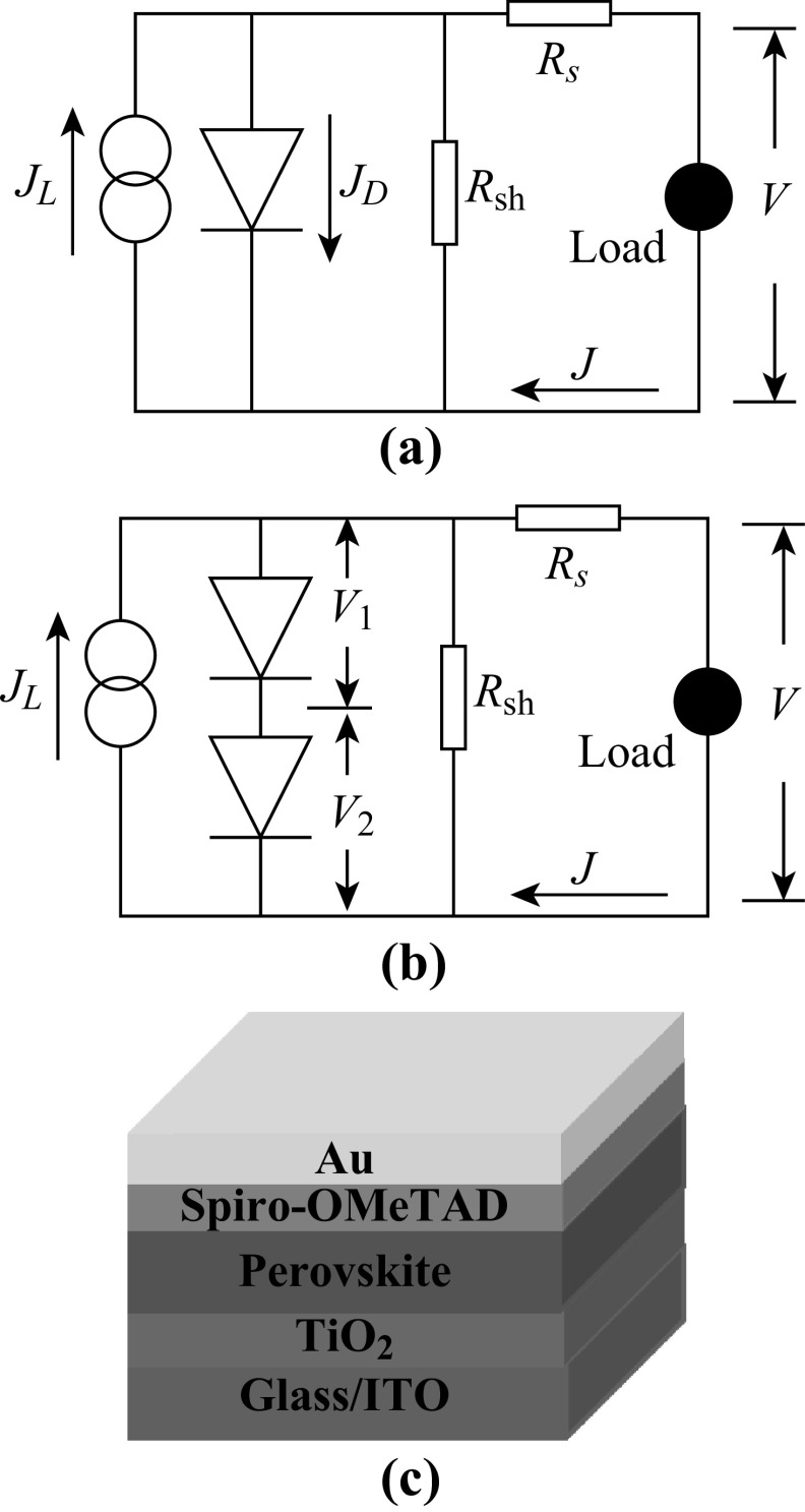
To date, planar-structured PSCs have been developing rapidly due to their various advantages of simple device structure, low-temperature processable fabrication and so on [10]. Nevertheless, in planar PSCs, the value of m obtained by single PN junction modeling does not fill in the theoretical expectation, indicating that the heterojunction property in planar PSCs further discussion [11, 12]. Generally, for a single heterojunction model, the ideal factor approaches to 1 when the carrier diffusion in the neutral region of semiconductors dominates the diode current through a PN junction. On the other hand, the ideal factor approaches to 2 when the diode current is dominated by carrier indirect recombination in depleted space-charge region [9]. Theoretically, the smaller value of m reflects the less carrier recombination induced by the interface defect state. In most cases, both diffusion and composite currents exist simultaneously, and therefore, the parameter m is in the range of 1–2. Interestingly, we note that, as shown in Table 1, most of the calculation results are larger than 2. Hence a single PN junction model (Fig. 1a) is not suitable to planar heterojunction PSCs [13, 14].
Table 1.
Calculated ideal factor (m) on planar heterojunction PSCs based on single PN junction model reported in the literatures
| Device architecture | Ideal factor (m) | References |
|---|---|---|
| ITO/PEDOT:PSS/CH3NH3PbI3-xClx/PCBM/PFN/Al | 2.3 | [16] |
| FTO/CH3NH3PbI3-xClx/Spiro-OMeTAD/Au | 3.39 | [38] |
| Mg-ZnO/CH3NH3PbI3-xClx/Spiro-OMeTAD/Au | 2.6–3.0 | [39] |
| ITO/PEDOT:PSS/Perovskite/PCBM/BCP/Ag | 2.2 | [40] |
| ITO/PEDOT:PSS/CH3NH3PbI3/C60/Al | 3.51 | [41] |
| FTO/Mg-TiO2/Perovskite/Spiro-OMeTAD/Au | 2.1 | [42] |
| FTO/TiO2/C60/(FA)x(MA)1-xPbI3/Spiro-OMeTAD/Au | 2.6–2.92 | [43] |
Fig. 1.
a Single PN junction model for PSCs and b new double PN junction model improved for planar perovskite solar cells with J L (the light induced current), J D (the dark current or the forward current of PN junction diode under the sunlight), R s (the series resistance), R sh (shunt resistance, a fictional parameter to represent the size of leakage current), J (output current of the cell) and V (voltage flowing through the external load). c Planar heterojunction perovskite solar cells with TiO2/CH3NH3PbI3-xClx/Sprio-OMeTAD/Au device architecture. (Color figure online)
In this work, we present a new equivalent circuit to investigate the heterojunction property for planar PSCs (in light and dark). Based on the new double heterojunction circuit, we found that smaller value of m reflects better PN junction quality in PSCs. Moreover, carrier recombination and transportation characteristics can be further explored by fitting J–V curve in dark with the new model for describing these important processes in efficient PSC devices.
Theoretical Background
Firstly, the rectification characteristic of heterojunction solar cell can be typically described by the Shockley diode equation (Eq. 1) [14],
| 1 |
where J D is the dark current, V is the applied voltage, J 0 is the reverse saturation current density, q is the elementary charge, m is the ideal factor of a heterojunction, K is the Boltzmann constant, T is the absolute temperature. Under the ideal condition of sunlight, photocurrent can be added into Eq. 1:
| 2 |
where J ph is the photocurrent. In fact, output current (J) in Eq. 2 is limited by internal resistance and leakage current in PSCs. Figure 1a presents ideal circuit model with a single PN junction, from which the J–V curve (in light) of heterojunction PSC can be further described with Eq. 3 [15],
| 3 |
where R s and R sh are the series and shunt resistance, respectively. Under the circumstances, R s, R sh, J 0 and m can be numerically obtained by simulation the J–V curves (both in light and dark) of PSCs with Eq. 3. The R s reflects the internal resistance, and R sh is a fiction parameter to represent the leakage current. The value of J 0 is directly related to the recombination rate, indicating the thermal emission rate of electrons from the valence band to the conduction band in light absorption layer [16], which also has an impact on the open-circuit voltage. Nevertheless, compared with R s and J 0, m, correlating with Shockley–Read–Hall recombination [6], is a rarely discussed parameter in PSCs when fitting J–V curves with using single PN junction model [17–20].
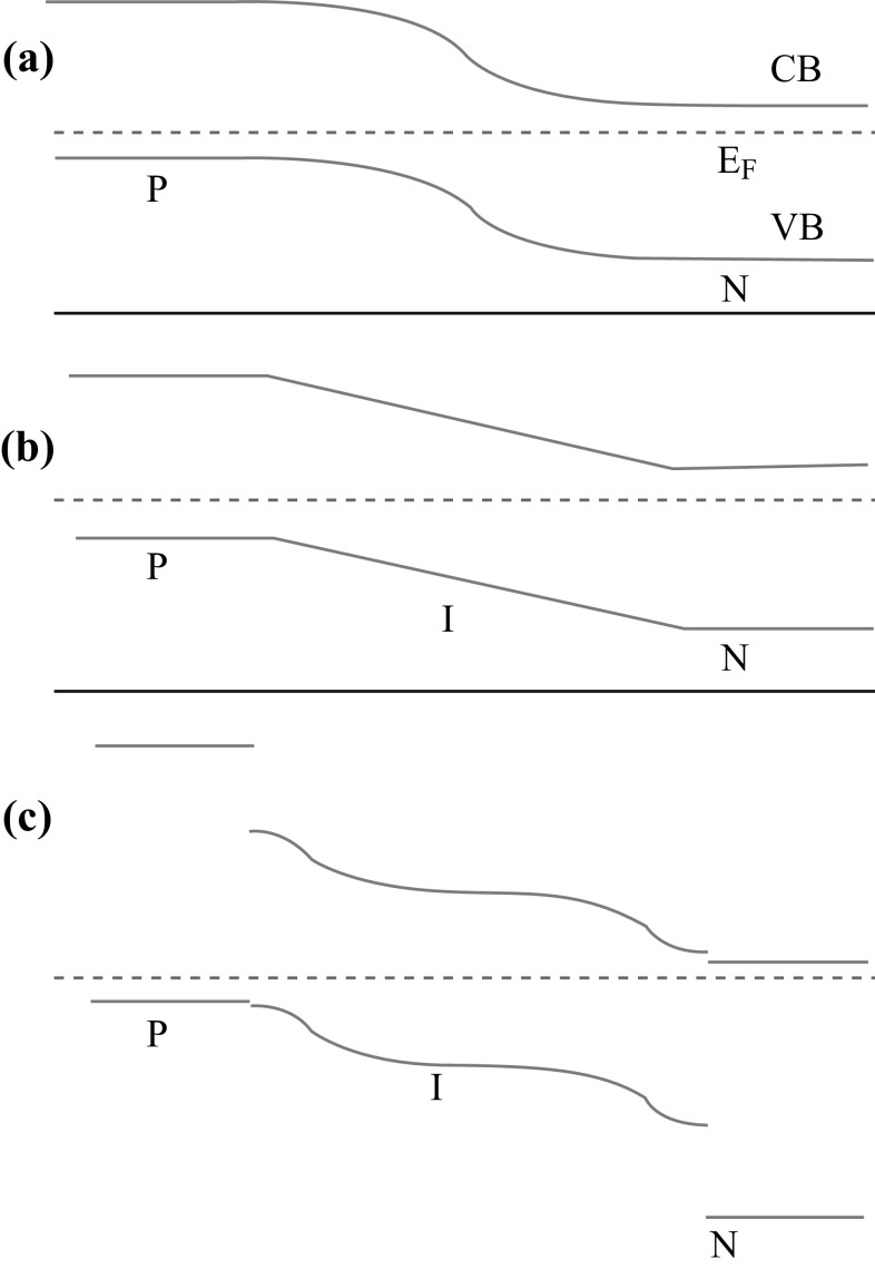
Compared to traditional P–I–N structure solar cells (‘a-Si: H’-like), inhomogeneous built-in field of PSCs results in different band structure (Fig. 2) [21, 22]. When the perovskite light absorption layer is sandwiched between n- and p-type charge selective contacts (Fig. 1c), two active junctions immediately form at the n-type electron transport layer (ETL) and the p-type hole transport layer (HTL) sides [22]. Therefore, we suggest two PN junctions in series for explaining planar heterojunction PSCs [23–27], rather than a single PN junction. Equation 4 is applied according to the equivalent circuit of double PN junction as shown in Fig. 1b:
| 4 |
Fig. 2.
Energy band diagram of different PN junction photovoltaic devices. a A PN junction solar cell. b A P–I–N solar cell with homogeneous built-in electric field. c CH3NH3PbI3-xClx perovskite-based cell with inhomogeneous built-in electric field. (Color figure online)
According to the characteristics of the series circuit, the current through the double PN junction should be identical (Eq. 5).
| 5 |
where m1, V 1, J 01, m 2, V 2, J 02 are diode ideality factor, voltage and reverse saturation current of ETL/perovskite and perovskite/HTL two PN junctions, respectively.
In this study, perovskite absorption layer acts as intrinsic semiconductor, which is fully depleted with highly doped P/N selective layers to form versatile PIN photovoltaics [28]. Considering the condition of J 01∝P n D p/Lp, J 02∝N p D n/Ln and a similar carrier density for electrons and holes [29, 30], the value of D p/L p can be approximately equal to D n/L n [31]. Therefore, the difference of the calculated J 01 and J 02 values lies in the same magnitude in this case according to the derivation process (Eq. 6).
| 6 |
Then Eq. 3 can be further revised as Eq. 7:
| 7 |
According to Eqs. 4–7, Eq. 8 and Eq. 9 can be inferred:
| 8 |
| 9 |
Equation 8 describes the J–V curve of planar PSCs under illumination. Since m in Eq. 3 includes the contribution from the double junctions, the sum of m 1 and m 2 can be in the range of 2–4. In short, the calculation results of m (~ 2–4) in Table 1 confirm the suitability of the proposed double heterojunction equivalent circuit for the planar PSC devices, with which carrier transportation (including direct recombination) and recombination (Shockley–Read–Hall recombination) processes can be preciously described.
Results and Discussion
In order to elucidate the effect of m on planar PSCs, we fabricated CH3NH3PbI3-based planar PSC devices with structure of ITO/TiO2/CH3NH3PbI3-xClx/Spiro-OMeTAD/Au using two-step deposition method [23], in which methylammonium chloride (MACl) was added to increase the perovskite films quality. Figure 3a shows the typical J–V characteristics of these devices under simulated sunlight at 100 mW cm−2 (AM 1.5G). Table 2 shows the photovoltaic parameters of devices with perovskite layers by varying MACl concentration.
Fig. 3.
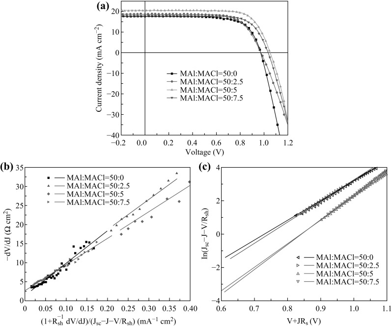
a Current–voltage curve for planar perovskite solar cells using TiO2/CH3NH3PbI3-xClx/Spiro-OMeTAD/Au architecture, the perovskite films prepared by mixing with different concentrations of Cl ions. The measurements are carried out under 100 mW cm−2. b Plots of (symbols) and the linear fitted curve (solid lines). c Plots of ln(J sc − J − V/R sh) versus V + JR s (symbols) and the linear fitted curve (solid lines). (Color figure online)
Table 2.
Photovoltaic performance of perovskite solar cells fabricated from doping varied MACl concentration
| MAI:MACl | J sc (mA cm−2) | V oc (V) | FF (%) | PCE (%) |
|---|---|---|---|---|
| 50:0 | 17.81 | 0.96 | 68.87 | 11.8 |
| 50:2.5 | 18.64 | 0.98 | 68.75 | 12.5 |
| 50:5 | 20.35 | 1.05 | 72.73 | 15.6 |
| 50:7.5 | 17.54 | 1.03 | 73.53 | 13.3 |
The addition of Cl− in the perovskite film significantly improved the efficiency of planar PSCs. The maximum performance was obtained for doping the appropriate amount of MACl (MAI:MACl = 50:5), which resulted in highly efficient devices exhibiting short-circuit current (J sc) of 20.35 mA cm−2, open-circuit voltage (V oc) of 1.05 V, fill factor (FF) of 72.73%, corresponding to PCE of 15.6%. The keys to improve the performance of CH3NH3PbI3-xClx devices were better crystallinity of perovskite film, pin hole-free coverage of the perovskite films and fewer interface defect states [32, 33].
We further fitted these J–V curves of devices in Fig. 3a to investigate the effect of doping Cl on perovskite layers by analyzing the parameters of R sh, R s, m 1 + m 2 and J 0. R sh can be calculated from the inverse of the slope of the J–V curves at 0 V [34]. The other three parameters (R s, m 1 + m 2, J 0) can be obtained through deduction of Eq. 8 as follows,
| 10 |
| 11 |
R s can be obtained by calculating the intercept of fitting curve of (Eq. 10) in Fig. 3b. Similarly, J 0 can be obtained by fitting the curve of ln(J sc − J − V/R sh) versus (V + JR s) (Eq. 11) in Fig. 3c. The value of (m 1 + m 2) can be simultaneously inferred from the slope of fitting curves (Eq. 11) in Fig. 3c. The calculation results of four parameters (R sh, R s, m 1 + m 2, J 0) are shown in Table 3.
Table 3.
R sh, R s, m 1 + m 2 and J 0 derived from Fig. 3b, c
| MAI:MACl | R sh (Ω cm2) | R s (Ω cm2) | m 1 + m 2 | J 0 (mA cm−2) |
|---|---|---|---|---|
| 50:0 | 840 | 1.41 | 3.27 | 1.69 × 10⁻⁴ |
| 50:2.5 | 5050 | 2.72 | 3.07 | 8.23 × 10⁻⁵ |
| 50:5 | 4280 | 2.61 | 2.66 | 6.89 × 10⁻⁶ |
| 50:7.5 | 3400 | 2.71 | 2.64 | 4.10 × 10⁻⁶ |
As shown in Table 3, the shunt resistance R sh dramatically increases from 840 to 5050, 4280, and 3400 Ω for addition of Cl ions (MAI:MACl from 50:0 to 50:7.5) in perovskite films. A larger R sh indicates less leakage current. This could be related to less pinholes for perovskite layers with Cl− than that without additives [32, 35]. It is significant that the ideal factor (m 1 + m 2) drastically decreases from 3.27 to 2.66 after adding Cl− and then keeps similar value of 2.66. The value of ideal factor (m 1 + m 2) is 3.27, 3.07, 2.66, and 2.64 for corresponding devices, respectively, which further conforms the feasibility of the double PN junction model. Smaller value of m 1 + m 2 indicates better PN junction quality [6]. The reverse saturation current (J 0) of corresponding devices was estimated to be 1.69 × 10⁻⁴, 8.23 × 10⁻⁵, 6.89 × 10⁻⁶ and 4.10 × 10⁻⁶ mA cm−2. The smaller J 0 is a sign of substantially suppression of the thermal emission rate of electrons from the VB to the CB [16], resulting in higher output voltage. This is verified with the V oc (being 1.05 V) of device with the suitable addition of Cl ions (MAI:MACl = 50:5) in perovskite layer, which is higher than devices without Cl. In short, the calculated R sh, m 1 + m 2 further indicates that larger short-circuit current (20.35 mA cm−2) for the device with Cl can be attributed to less carrier recombination and loss in ETL/perovskite and perovskite/HTL interfaces.
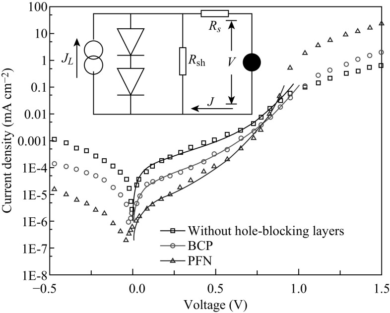
The dark current was fitted with Eq. 3 (single PN junction model); however, very limited information can be obtained except of three parameters (m, J 0, R s) [7]. Furthermore, in the exponential coordinates, the dark current curve slope varies with the increase in voltage, reflecting different physical processes. This physical process cannot be reflected by Eq. 3 (single PN junction model). In fact, as shown in Fig. 4a, regions A, B, C of dark current is related to shunt current, recombination current and diffusion current, respectively. At last, above the built-in potential at about 1.2 V in region D, the effect of the recombination current is negligible, and the curve is determined only by the diffusion current, limited by the series resistance (R s) of the cell [14]. In order to more accurate quantitative analysis of the dark J–V characteristic in regions A, B, C in the perovskite solar cells, regardless of region D, Eq. 8 can be futherly deduced in dark (not consider J L, R s):
| 12 |
Fig. 4.
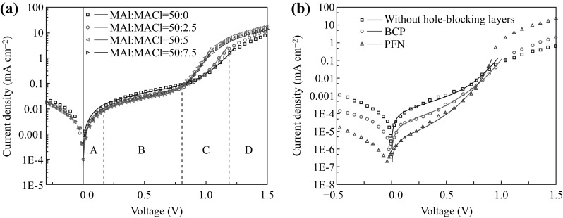
Plots of dark current of planar PSCs as well as fitting curve by using Eq. 13. a The device structure is shown in Fig. 1c, the perovskite films prepared by mixing with different concentrations of Cl ions. b The device structure is PEDOT:PSS/CH3NH3PbI3-xClx/PCBM/hole-blocking layer/Al, with the original data coming from the Ref. [8]. The inset regions A, B, C, D are mainly determined by shunt current, recombination current in diode space-charge region, diffusion current, diode diffusion current limited by series resistance, respectively. (Color figure online)
In region A of Fig. 4a, the dark current is mainly affected by the shunt current under the small applied bias voltage. With the bias voltage increase, recombination current is much larger than diffusion current in dark J–V characteristics of planar PSCs, as shown in region B of Fig. 4a. The slope of region B is less than slope of region C, and the steep increment of the current results from a diffusion-dominated current [14]. The dark current–voltage characteristic is in a single exponential relationship in region B and region C, respectively.
In order to quantitative calculate diffusion current and recombination current, respectively, Eq. 12 is further rewritten by taking into account the heterojunction diffusion model [29, 30]:
| 13 |
In Eq. 13, the first term is the shunt current corresponding to region A in Fig. 4a. The second term is the recombination current (Shockley–Read–Hall recombination), m 1r = 2. The third term is the diffusion current (including carrier directly recombination), m 1d = 1 [14, 36, 37]. According to Eqs. 9, 13 can be furtherly derived:
| 14 |
In Eq. 14, m r = m 1r + m 2r = 4, m d = m 1d + m 2d = 2. The dark current in Fig. 4a can be fitted by Eq. 14. The calculation results of three parameters (R sh, J r, J d) are shown in Table 4.
Table 4.
| MAI:MACl | R sh (MΩ cm2) | J r (mA cm−2) | J d (mA cm−2) |
|---|---|---|---|
| 50:0 | 12 | 1 × 10⁻⁵ | 5 × 10⁻¹¹ |
| 50:2.5 | 16 | 9 × 10⁻⁶ | 3 × 10⁻¹⁰ |
| 50:5 | 20 | 8 × 10⁻⁶ | 5 × 10⁻⁹ |
| 50:7.5 | 19 | 8 × 10⁻⁶ | 3 × 10⁻⁹ |
We fit the dark current of inverted planar heterojunction PSCs in other literatures in order to further verify the formula based on double PN junction equivalent circuit (Fig. 1b) [8].
As shown in Table 5, the parameter R sh of inverted planar PSCs with different hole-blocking layers is 1, 5, and 35 MΩ cm2. The recombination current (J r) of corresponding devices is 3 × 10⁻⁶, 1.5 × 10⁻⁶, and 5 × 10⁻⁷ mA cm−2. Both of them indicate that hole-blocking layer blocks hole injection into the diode, effectively reducing the shunt current and recombination current. Compared to the BCP, the device with PFN shows better hole-blocking property. The same conclusion obtained by comparing the dark current at − 100 mV as discussed in the literatures. Meanwhile, the devices without hole-blocking layer showed larger dark current under reverse bias, mainly due to the larger hole injection into the diode [8]. Moreover, the PFN enhanced electron injection and extraction, which can be verified by drastically increased diffusion current J d (from 8 × 10⁻¹⁰ to 1 × 10⁻⁹ mA cm−2). This conclusion confirms the speculation in the literature: PFN improves the electron injection and extraction in PSC devices [8]. Therefore, the new model proposed in this study can be universal and effective to analyze carrier recombination and transportation.
Table 5.
R sh, J r, J d derived from fitting dark current of inverted planar PSCs in Fig. 4b
| Hole-blocking layer | R sh (MΩ cm2) | J r (mA cm−2) | J d (mA cm−2) |
|---|---|---|---|
| Without | 1 | 3 × 10⁻⁶ | 8 × 10⁻¹⁰ |
| BCP | 5 | 1.5 × 10⁻⁶ | 4 × 10⁻¹⁰ |
| PFN | 35 | 5 × 10⁻⁷ | 1 × 10⁻⁹ |
Conclusion
In conclusion, we built up a double PN junction equivalent circuit to fit J–V curves of P–I–N planar structure heterojunction PSCs. The new method focuses on the relationship between the diode ideal factor and the carrier recombination from the interface defects. By varying Cl− content in the CH3NH3PbI3 perovskite film, we found that the value of m drastically diminished (decreased) with the perovskite film quality improvement. In order to quantitatively analyze the correlation mechanism of dark current under different bias voltages, a new equation based on the double PN junction equivalent circuit has been proposed to analyze the dark current–voltage curve. Consequently, carrier recombination and loss reduction could be reflected in R sh and J r. The carrier transmission could be reflected on the parameter J d. Based on the double PN junction equivalent circuit, the J–V curve in light and in dark could be fitted, respectively, helping us analyze the working mechanism and improve the efficiency of planar PSCs.
Acknowledgements
Financial support from the 973 Program of China (No. 2014CB643506 and 2013CB922104), the China Scholarship Council (No. 201506165038), the Natural Science Foundation of China (No. 21673091), the Natural Science Foundation of Hubei Province (No. ZRZ2015000203), Technology Creative Project of Excellent Middle and Young Team of Hubei Province (No. T201511) and the Wuhan National High Magnetic Field Center (2015KF18) is acknowledged.
References
- 1.Kagan CR, Mitzi DB, Dimitrakopoulos CD. Organic-inorganic hybrid materials as semiconducting channels in thin-film field-effect transistors. Science. 1999;286(5441):945–947. doi: 10.1126/science.286.5441.945. [DOI] [PubMed] [Google Scholar]
- 2.Kim HS, Lee CR, Im JH, Lee KB, Moehl T, et al. Lead iodide perovskite sensitized all-solid-state submicron thin film mesoscopic solar cell with efficiency exceeding 9% Sci. Rep. 2012;2(8):591. doi: 10.1038/srep00591. [DOI] [PMC free article] [PubMed] [Google Scholar]
- 3.Burschka J, Pellet N, Moon SJ, Humphry-Baker R, Gao P, Nazeeruddin MK, Gratzel M. Sequential deposition as a route to high-performance perovskite-sensitized solar cells. Nature. 2013;499(7458):316–319. doi: 10.1038/nature12340. [DOI] [PubMed] [Google Scholar]
- 4.Khan F, Singh SN, Husain M. Determination of diode parameters of a silicon solar cell from variation of slopes of the I-V curve at open circuit and short circuit conditions with the intensity of illumination. Semicond. Sci. Tech. 2010;25(1):015002. doi: 10.1088/0268-1242/25/1/015002. [DOI] [Google Scholar]
- 5.Hegedus SS, Shafarman WN. Thin-film solar cells: device measurements and analysis. Prog. Photovoltaics. 2004;12(2–3):155–176. doi: 10.1002/pip.518. [DOI] [Google Scholar]
- 6.Kim J, Yun JH, Kim H, Cho Y, Park HH, Kumar MMD, Yi J, Anderson WA, Kim DW. Transparent conductor-embedding nanocones for selective emitters: optical and electrical improvements of Si solar cells. Sci. Rep. 2015;5(1):9256. doi: 10.1038/srep09256. [DOI] [PMC free article] [PubMed] [Google Scholar]
- 7.Shi JJ, Dong J, Lv ST, Xu YZ, Zhu LF, et al. Hole-conductor-free perovskite organic lead iodide heterojunction thin-film solar cells: high efficiency and junction property. Appl. Phys. Lett. 2014;104(6):063901. doi: 10.1063/1.4864638. [DOI] [Google Scholar]
- 8.Dou LT, Yang Y, You JB, Hong ZR, Chang WH, Li G, Yang Y. Solution-processed hybrid perovskite photodetectors with high detectivity. Nat. Commun. 2014;5:5404. doi: 10.1038/ncomms6404. [DOI] [PubMed] [Google Scholar]
- 9.Li Y, Xu Z, Zhao SL, Qiao B, Huang D, et al. Highly efficient P–I–N perovskite solar cells utilizing novel low-temperature solution-processed hole transport materials with linear pi-conjugated structure. Small. 2016;12(35):4902–4908. doi: 10.1002/smll.201601603. [DOI] [PubMed] [Google Scholar]
- 10.Meng L, You JB, Guo TF, Yang Y. Recent advances in the inverted planar structure of perovskite solar cells. Accounts Chem. Res. 2016;49(1):155–165. doi: 10.1021/acs.accounts.5b00404. [DOI] [PubMed] [Google Scholar]
- 11.Zhou Z, Xu J, Xiao L, Chen J, Tan ZA, Yao JX, Dai SY. Efficient planar perovskite solar cells prepared via a low-pressure vapor-assisted solution process with fullerene/TiO2 as an electron collection bilayer. RSC Adv. 2016;6(82):78585–78594. doi: 10.1039/C6RA14372E. [DOI] [Google Scholar]
- 12.Liu D, Liu C, Wu LL, Li W, Chen F, Xiao BQ, Zhang JQ, Feng LH. Highly reproducible perovskite solar cells with excellent CH3NH3PbI3-xClx film morphology fabricated via high precursor concentration. RSC Adv. 2016;6(56):51279–51285. doi: 10.1039/C6RA07359J. [DOI] [Google Scholar]
- 13.Wang MK, Yim WL, Liao PZ, Shen Y. Temperature dependent characteristics of perovskite solar cells. ChemistrySelect. 2017;2(16):4469–4477. doi: 10.1002/slct.201700776. [DOI] [Google Scholar]
- 14.Wetzelaer GJAH, Scheepers M, Sempere AM, Momblona C, Avila J, Bolink HJ. Trap-assisted non-radiative recombination in organic-inorganic perovskite solar cells. Adv. Mater. 2015;27(11):1837–1841. doi: 10.1002/adma.201405372. [DOI] [PubMed] [Google Scholar]
- 15.Lu JF, Bai J, Xu XB, Li ZH, Cao K, Cui J, Wang MK. Alternate redox electrolytes in dye-sensitized solar cells. Chin. Sci. Bull. 2012;57(32):4131–4142. doi: 10.1007/s11434-012-5409-3. [DOI] [Google Scholar]
- 16.You JB, Yang YM, Hong ZR, Song TB, Meng L, et al. Moisture assisted perovskite film growth for high performance solar cells. Appl. Phys. Lett. 2014;105(18):183902. doi: 10.1063/1.4901510. [DOI] [Google Scholar]
- 17.Zhu WD, Bao CX, Wang Y, Li FM, Zhou XX, et al. Coarsening of one-step deposited organolead triiodide perovskite films via Ostwald ripening for high efficiency planar-heterojunction solar cells. Dalton Trans. 2016;45(18):7856–7865. doi: 10.1039/C6DT00900J. [DOI] [PubMed] [Google Scholar]
- 18.Li XD, Liu XH, Wang XY, Zhao LX, Jiu TG, Fang JF. Polyelectrolyte based hole-transporting materials for high performance solution processed planar perovskite solar cells. J. Mater. Chem. A. 2015;3(29):15024–15029. doi: 10.1039/C5TA04712A. [DOI] [Google Scholar]
- 19.Li EZ, Guo Y, Liu T, Hu W, Wang N, He HC, Lin H. Preheating-assisted deposition of solution-processed perovskite layer for an efficiency-improved inverted planar composite heterojunction solar cell. RSC Adv. 2016;6(37):30978–30985. doi: 10.1039/C5RA27434F. [DOI] [Google Scholar]
- 20.Yuan S, Qiu ZW, Zhang HL, Gong HB, Hao YF, Cao BQ. Oxygen influencing the photocarriers lifetime of CH3NH3Pbl3-xClx film grown by two-step interdiffusion method and its photovoltaic performance. Appl. Phys. Lett. 2016;108(3):033904. doi: 10.1063/1.4940368. [DOI] [Google Scholar]
- 21.Nelson J. The Physics of Solar Cells. London: Imperial College Press; 2003. [Google Scholar]
- 22.Edri E, Kirmayer S, Mukhopadhyay S, Gartsman K, Hodes G, Cahen D. Elucidating the charge carrier separation and working mechanism of CH3NH3PbI3-xClx perovskite solar cells. Nat. Commun. 2014;5:3461. doi: 10.1038/ncomms4461. [DOI] [PubMed] [Google Scholar]
- 23.Shai XX, Zuo LJ, Sun PY, Liao PZ, Huang WC, et al. Efficient planar perovskite solar cells using halide Sr-substituted Pb perovskite. Nano Energy. 2017;36:213–222. doi: 10.1016/j.nanoen.2017.04.047. [DOI] [Google Scholar]
- 24.Cui J, Li PF, Chen ZF, Cao K, Li D, et al. Phosphor coated NiO-based planar inverted organometallic halide perovskite solar cells with enhanced efficiency and stability. Appl. Phys. Lett. 2016;109(17):171103. doi: 10.1063/1.4965838. [DOI] [Google Scholar]
- 25.Li D, Cui J, Li H, Huang DK, Wang MK, Shen Y. Graphene oxide modified hole transport layer for CH3NH3PbI3 planar heterojunction solar cells. Sol. Energy. 2016;131:176–182. doi: 10.1016/j.solener.2016.02.049. [DOI] [Google Scholar]
- 26.Luo H, Lin XH, Hou X, Pan LK, Huang SM, Chen XH. Efficient and air-stable planar perovskite solar cells formed on graphene-oxide-modified PEDOT:PSS hole transport layer. Nano-Micro Lett. 2017;9(4):39. doi: 10.1007/s40820-017-0140-x. [DOI] [PMC free article] [PubMed] [Google Scholar]
- 27.Li D, Cui J, Zhang H, Li H, Wang MK, Shen Y. Effect of hole transport layer in planar inverted perovskite solar cells. Chem. Lett. 2016;45(1):89–91. doi: 10.1246/cl.150888. [DOI] [Google Scholar]
- 28.Yan KY, Wei ZH, Zhang TK, Zheng XL, Long MZ, et al. Near-infrared photoresponse of one-sided abrupt MAPbI3/TiO2 heterojunction through a tunneling process. Adv. Funct. Mater. 2016;26(46):8545–8554. doi: 10.1002/adfm.201602736. [DOI] [Google Scholar]
- 29.Streetman BG, Banerjee SK. Solid State Electronic Devices. Upper Saddle River: Prentice Hall; 2006. [Google Scholar]
- 30.Liu EK, Zhu BS, Luo JS. The Physics of Semiconductors. Beijing: Publishing House of Electronics Industry; 2012. [Google Scholar]
- 31.Stranks SD, Eperon GE, Grancini G, Menelaou C, Alcocer MJP, Leijtens T, Herz LM, Petrozza A, Snaith HJ. Electron-hole diffusion lengths exceeding 1 micrometer in an organometal trihalide perovskite absorber. Science. 2013;342(6156):341–344. doi: 10.1126/science.1243982. [DOI] [PubMed] [Google Scholar]
- 32.Tripathi N, Yanagida M, Shirai Y, Masuda T, Han LY, Miyano K. Hysteresis-free and highly stable perovskite solar cells produced via a chlorine-mediated interdiffusion method. J. Mater. Chem. A. 2015;3(22):12081–12088. doi: 10.1039/C5TA01668A. [DOI] [Google Scholar]
- 33.Hutter EM, Eperon GE, Stranks SD, Savenije TJ. Charge carriers in planar and meso-structured organic-inorganic perovskites: mobilities, lifetimes, and concentrations of trap states. J. Phys. Chem. Lett. 2015;6(15):3082–3090. doi: 10.1021/acs.jpclett.5b01361. [DOI] [PubMed] [Google Scholar]
- 34.Min J, Zhang ZG, Hou Y, Ramirez Quiroz CO, Przybilla T, et al. Interface engineering of perovskite hybrid solar cells with solution-processed perylene-diimide heterojunctions toward high performance. Chem. Mater. 2015;27(1):227–234. doi: 10.1021/cm5037919. [DOI] [Google Scholar]
- 35.Edri E, Kirmayer S, Kulbak M, Hodes G, Cahen D. Chloride inclusion and hole transport material doping to improve methyl ammonium lead bromide perovskite-based high open-circuit voltage solar cells. J. Phys. Chem. Lett. 2014;5(3):429–433. doi: 10.1021/jz402706q. [DOI] [PubMed] [Google Scholar]
- 36.Wurfel U, Neher D, Spies A, Albrecht S. Impact of charge transport on current-voltage characteristics and power-conversion efficiency of organic solar cells. Nat. Commun. 2015;6:6951. doi: 10.1038/ncomms7951. [DOI] [PMC free article] [PubMed] [Google Scholar]
- 37.Sze SM, Ng KK. Physics of Semiconductor Devices. New York: Wiley; 1981. [Google Scholar]
- 38.Ke WJ, Fang GJ, Wan JW, Tao H, Liu Q, et al. Efficient hole-blocking layer-free planar halide perovskite thin-film solar cells. Nat. Commun. 2015;6:6700. doi: 10.1038/ncomms7700. [DOI] [PubMed] [Google Scholar]
- 39.Dong J, Shi JJ, Li DM, Luo YH, Meng QB. Controlling the conduction band offset for highly efficient ZnO nanorods based perovskite solar cell. Appl. Phys. Lett. 2015;107(7):073507. doi: 10.1063/1.4929435. [DOI] [Google Scholar]
- 40.Qing J, Chandran HT, Cheng YH, Liu XK, Li HW, Tsang SW, Lo MF, Lee CS. Chlorine incorporation for enhanced performance of planar perovskite solar cell based on lead acetate precursor. ACS Appl. Mater. Interface. 2015;7(41):23110–23116. doi: 10.1021/acsami.5b06819. [DOI] [PubMed] [Google Scholar]
- 41.Wang YK, Yang DZ, Zhou XK, Alshehri SM, Ahamad T, Vadim A, Ma DG. Vapour-assisted multi-functional perovskite thin films for solar cells and photodetectors. J. Mater. Chem. C. 2016;4(31):7415–7419. doi: 10.1039/C6TC00747C. [DOI] [Google Scholar]
- 42.Zhang HY, Shi JJ, Xu X, Zhu LF, Luo YH, Li DM, Meng QB. Mg-doped TiO2 boosts the efficiency of planar perovskite solar cells to exceed 19% J. Mater. Chem. A. 2016;4(40):15383–15389. doi: 10.1039/C6TA06879K. [DOI] [Google Scholar]
- 43.Chen J, Xu J, Xiao L, Zhang B, Dai SY, Yao JX. Mixed-organic-cation (FA)x(MA)1-xPbI3 planar perovskite solar cells with 16.48% efficiency via a low-pressure vapor-assisted solution process. ACS Appl. Mater. Interface. 2017;9(3):2449–2458. doi: 10.1021/acsami.6b13410. [DOI] [PubMed] [Google Scholar]


