Abstract
The nitrogen-vacancy (NV) centre in diamond is a promising candidate for quantum computing applications and magnetic sensing applications, because it is an atomic-scale defect with stable coherence time (T2) and reliable accessibility at room temperature. We demonstrated a method for improving the NV spin properties (the full width half maximum (FWHM) value of the magnetic resonance spectrum and T2) through a near-field (NF) etching method under ambient conditions. The NF etching method, based on a He-Cd ultraviolet laser (325 nm), which is longer than the absorption edge of the oxygen molecule, enabled selective removal of defects on the nanodiamond surface. We observed a decrease in the FWHM value close to 15% and an increase in T2 close to 25%. Since our technique can be easily reproduced, a wide range of NV centre applications could be improved, especially magnetic sensing applications. Our results are especially attractive, because they have been obtained under ambient conditions and only require a light source with wavelength slightly above the O2 absorption edge.
Introduction
The nitrogen-vacancy (NV) centre has emerged as a promising candidate for nanoscale sensing applications in physics and biology1–5. Here, sensing is commonly realized by reading out the NV spin resonances (e.g., optically-detected magnetic resonance (ODMR)) and its shift under magnetic fields, with the magnetic sensitivity being dependent on the NV coherence properties6. However, sensing can also be realized by directly observing the change in the NV coherence time when close to magnetic molecules7. This spin-coherence-reliant approach has been well summarized under the term quantum sensing8. However, for either approach, the importance of T2 prevails.
Furthermore, to bring quantum computing closer to reality, it is critical to find a qubit candidate with long enough coherence times. The coherence time (T2) is the time for which the system stays in a superposition, and can thus be effectively used for the transmission of quantum information. One of the criteria—introduced by D. DiVincenzo for a system to perform quantum operations—is a coherence time that is much longer than the gate operation time9. Unfortunately our current qubits are relatively volatile, meaning that they lose their quantum information rather quickly. Hence, the current goal is to push coherence times to their maximum. Although it was possible to achieve coherence times well into the minute range, by using ionized donors combined with optical methods and dynamical decoupling10, it is still of common interest to find a more convenient qubit candidate, which can be used under ambient conditions. One of these candidates is the NV centre in diamond, which naturally exhibits excellent characteristics, such as long electron-spin coherence and relaxation times as well as unique optical and magnetic properties11–16. The NV centre can be initialized, driven, and read out17–19 by using external optical and microwave fields. Under room temperature, the T2 of the NV centre typically lies in the microsecond range20, with the benchmark currently being 1.8 ms achieved by using an ultrapure isotopically controlled single-crystal chemical vapour deposition (CVD) method21. From a material point of view, this can be done by purifying the diamond first by decreasing the amount of additional defects in the crystal. It can further be purified by isotopically engineering the carbon and making the effort to have only the nuclear-spin-free 12C isotopes in the crystal22. A previous research group has successfully improved the coherence properties of diamond bulk NV-centres via surface etching (wet oxidative chemistry combined with annealing at 465 °C23). However, so far there have been no reports on the effect of etching on the coherence properties of nanodiamond NV centres, although nanodiamonds are crucial for sensing applications24.
T2 is limited by fast fluctuations (that cannot be refocused by Hahn-echo), which can originate from flip-flops of spins at the surface of the diamond. Hence, we assume that T2 is directly proportional to the amount of noise on the surface of the diamond. It should be noted that a recent study by Knowles et al.25 suggested that the main contribution to the NV centre decoherence comes from nearby nitrogen impurities; however, in this paper, we would like to focus on improving the surface conditions, as this could also be useful for applications not based on the NV centres. Besides the known methods for reducing the impact of surface noise, such as dynamical decoupling26, previous studies indicate that ultraviolet (UV) lasers (325 nm) can induce ultra-fine surface etching (near-field (NF) etching) on various samples, including diamond, under ambient conditions27. We demonstrated that under sufficiently long-wavelength UV laser-light (325 nm) illumination, it was possible to reduce the dimensions of the nanodiamonds, alongside a decrease in the full width at half maximum (FWHM) value of the ODMR spectrum, and an increase in T2. These results indicate that the surface etching achieved with the NF etching method results in the removal of parasitic magnetic fields and optical noise from the nanodiamond surface.
Results
Structural change in nanodiamonds through a near-field etching approach
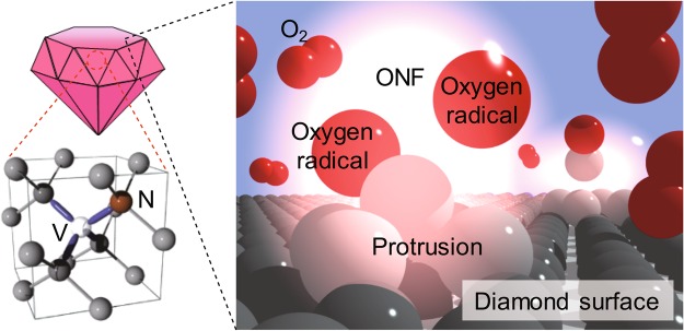
To improve the spin properties of nanodiamond NV, we performed NF etching on the NV nanodiamonds. Under far-field light irradiation, charges are generated in sub-wavelength objects (nano-scale surface protrusions), resulting in the generation of optical near-fields (ONF), which interact with matter within sub-wavelength distances (such as gas molecules). ONFs have non-uniform electric fields, which can excite dipole-forbidden states of molecules and trigger second harmonic generations28. Because the laser photon energy is lower than the O2 binding energy (5.12 eV), the presence of ONFs is required for the dissociation of O2 molecules29–33. In other words, the selectiveness of the photo-dissociation enables a controlled etching of the surface protrusions. Previous studies already showed that this technique is able to etch and improve various substrates, including diamond substrates34 as well as nanodiamonds35.
In the NF etching experiment (Fig. 1), the NV nanodiamonds with a diameter of approximately 200 nm36 were irradiated by a He-Cd laser with a wavelength of 325 nm (3.81 eV, lower than the dissociation energy of O2, 5.12 eV) with 8 mW under atmospheric conditions and ambient O2 molecules as the source for the etching effect. The nanodiamonds (see Methods) were dispersed on a Si substrate before being perpendicularly illuminated with a UV laser. While being illuminated with the UV laser, the nanodiamonds appeared to be etched on their surface and, over time, slowly reduced in size. Prior to evaluating how NF etching affects the spin properties of nanodiamond NV, we first evaluated the general effectiveness of NF etching on nanodiamonds, i.e., checking the degree of structural change.
Figure 1.
A schematic view of NF etching on the NV nanodiamonds. Optical near-fields (ONF) are generated by the He-Cd laser (3.81 eV) irradiation at the nanoscale protrusions on the nanodiamond surface. Since the photon energy is below the O2 dissociation energy (5.12 eV), O2 is only dissociated at the protrusions, thus allowing selective etching.
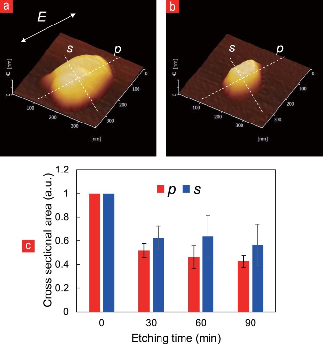
Figure 2 shows the extent of the size reduction of the nanodiamond during He-Cd laser illumination. The two dashed-lines over the nanodiamonds represent the parallel-axis (p) and perpendicular-axis (s) to the He-Cd laser polarization (E). The atomic force microscope (AFM) images of the nanodiamond show a significant size reduction over a total timespan (90 min) of He-Cd laser illumination (Fig. 2a,b). In Fig. 2c we observe the average change of eight individual nanodiamonds for the cross-sectional area along the p-axis and s-axis over time (0, 30, 60, and 90 min), since previous research37 indicated the structural change to be caused mainly along the laser polarization-parallel-axis (p). In accordance with the previous study38, the initial 30 min apparently account for the highest etching rate, while after that, the NF etching effect appears to saturate (Fig. 2c). Within the first time interval (0–30 min) the area has been roughly halved (52% (p-axis) and 62% (s-axis)). Nevertheless, for continued illumination longer than 30 min, the extent of size reduction caused by NF etching appears more subtle, with the (30–60 min) and (60–90 min) intervals showing a size reduction along the p-axis to 46% and 42% and along the s-axis to 63% and 56%, respectively.
Figure 2.
AFM images of the nanodiamonds, comparing their size before (a) and after 90 min (b) of He-Cd laser illumination. The comparison in size has been further examined through AFM in (c) by comparing the cross-sectional area of the nanodiamonds along the presumed parallel laser polarization axis (p-axis) and the presumed perpendicular laser polarization axis (s-axis), showing a general decrease in the cross-sectional area over illumination time.
Evaluation of the effect of NF etching on NV spin properties
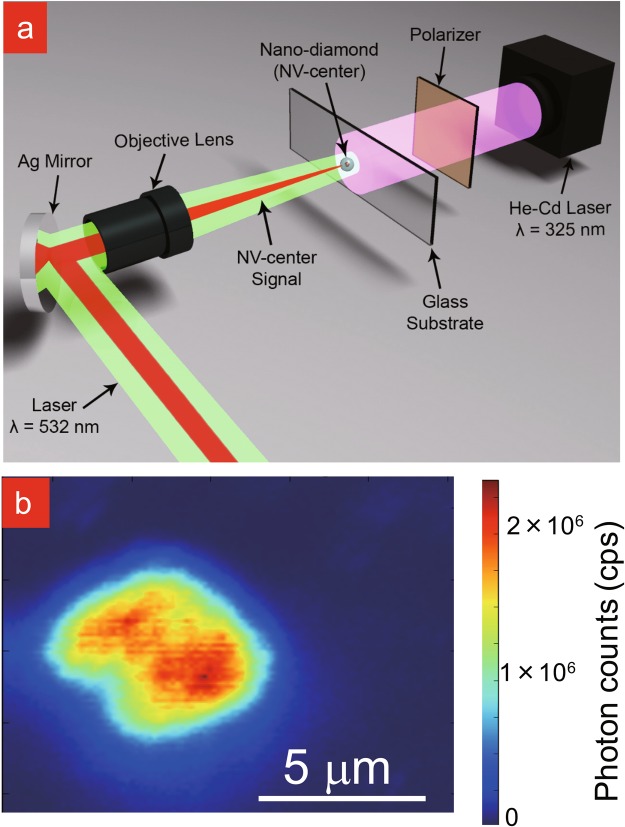
To evaluate the effect of NF etching on the NV nanodiamonds, we compared the ODMR- and Hahn-echo T2 signal, through the confocal setup, for an individual nanodiamond between the before and after NF etching cases (Fig. 3a). This sequence was repeated every 30 min, thus enabling us to observe slow changes in nanodiamond size and NV spin properties with etching time for the same nanodiamonds (Fig. 3b).
Figure 3.
(a) Schematic view of the experimental setup. (b) Typical 2D fluorescence mapping of NV nanodiamonds (500 NV).
Figure 4a shows the time-averaged ODMR spectra for 500 s. Note that all ODMR spectra were obtained from the same nanodiamond containing 500 NV. As shown in Fig. 4a, we observed a decrease in the FWHM of the ODMR spectrum with increasing etching durations. By single Lorentzian fitting of the raw ODMR spectrum in Fig. 4a, we gained a more detailed perspective of the effective change in the FWHM values, as shown in Fig. 4b. The dots represent its average FWHM value. The error bar hereby represents the variance of the raw data points from their Lorentzian fitting in Fig. 4a. Figure 4b shows that the initial FWHM of approximately 23 MHz decreases gradually until it bottomed at around 19.6 MHz after an etching time of 90 min (~15% reduction compared to the initial value). However, longer NF etching times seem to have a somewhat opposite effect on the FWHM value, increasing it up to approximately 20.5 MHz for etching times close to 150 min. Although the FWHM was reduced, the contrast was reduced as well. The reduction of the contrast should be due to the reduction of the number of NV centres along the size reduction of the nanodiamonds. However, if we prepare a larger nanodiamond and take into account the NF etching depth, we could achieve a similar contrast as that before the etching. Therefore, we believe that a higher sensitivity with the reduction of FWHM can be achieved while keeping the ODMR contrast constant.
Figure 4.
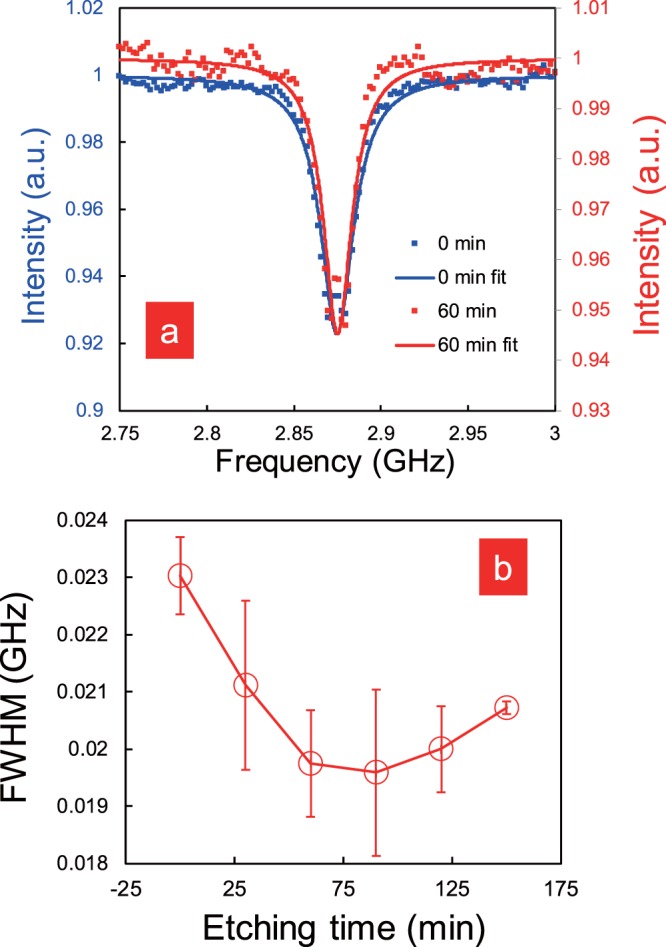
(a) ODMR spectra before (blue solid line (left-hand vertical axis); 0 min.) and after (red solid line (right-hand vertical axis); 60 min) NF etching. (b) FWHM value of the ODMR spectrum as a function of the NF etching time.
Figures 5a–c show the typical Hahn-echo signal before and after NF etching. Each signal was accumulated for 1000 s. Note that all the Hahn-echo signals were obtained from the same nanodiamond containing single NV. Figure 5b appears to have a longer coherence time (T2) than Figs. 5a and 5c. From our original coherence data (splatters in Figs. 5a–c, we extracted T2 by fitting the data to an exponential function f(t) = exp[−t/T2]. To visualize the improvement in T2, we plotted T2 as a function of the NF etching time, as shown in Fig. 5d. The nanodiamonds used for the Hahn-echo measurement contained only a single NV centre on average and the error bar represents the variance of the raw data from their exponential fit in Figs 5a–c. Results in Fig. 5d show that T2 increases after being exposed to NF etching. The initial T2 (~1600 ns) improved with increasing NF etching times and peaked (~2000 ns) after approximately 60 min, corresponding to an increase of approximately 25%. After that T2 dropped significantly with longer NF etching durations until it hit bottom at approximately 1400 ns (~87.5% of its initial value) for etching times longer than 120 min.
Figure 5.
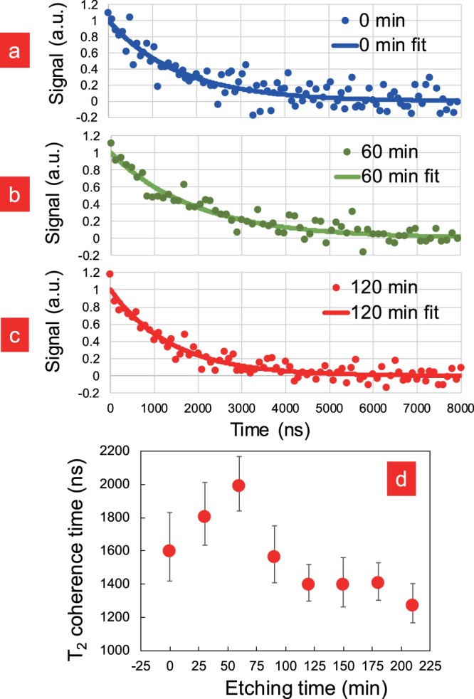
Normalized Hahn-echo signals (dots) before (a), after 60 min (b), and after 120 min (c) of NF etching, with exponential fitting curves (lines). (d) The measured Hahn-echo T2 of the single-NV nanodiamond as a function of the NF etching time.
Discussion
Our results demonstrate that the FWHM value as well as the spin coherence time T2 can both be improved within an early timeframe of NF etching. The results from Figs 4b and 5d suggest that when applying NF etching, there is a specific exposure time, which will result in optimal values for both the FWHM value and spin coherence time T2.
The change in the FWHM value (Fig. 4b) can be explained as follows. The ODMR spectrum depends strongly on the presence of paramagnetic noise on the nanodiamond surface, especially when the NV centre exists close to the diamond surface39, though generally, the FWHM value cannot be reduced beyond a certain limit, which is set by the internal distortion of the nanodiamond.
The change in T2 (Fig. 5d) can be explained in a manner similar to the FWHM change. It should be derived from the change in the magnetic environment surrounding the NV centre. NF etching has the ability to remove surface impurities, such as structural defects and termination groups, which are known to influence the NV spin. Surface defects create a defect level in the band gap of diamond, which will be occupied by an electron whose spin will influence the NV centre40. Surface termination41 groups can influence the NV centre as well, as previous research has found that atoms attached to the surface of the NV centre in diamond can affect its spin coherence time42. Dangling bonds on the nanodiamond surface are another problem, since they are not able to covalently bond with another partner and are thus occupied by unpaired electrons with spins43. Oxygen molecules adsorbed onto the diamond surface can affect the NV-centre spin due to their paramagnetic nature44. Thus, the initial increase in T2 can be explained by the removal of surface defects and termination groups. On the other hand, the decrease in T2 could have been caused by an increase in the number of dangling bonds and oxygen molecules adsorbed onto the nanodiamond surface. Eliminating the termination group, as well as removing carbon atoms, leaves energetically unstable dangling bonds on the nanodiamond surface, attracting reactive compounds in the air, which further affect the NV spin. Although NF etching visibly changes the structure of the nanodiamonds, we can generally exclude the possibility that the single NV centre was removed (due to the measured NV signal over the whole etching distance, Fig. 5). The different peak times in Figs 4b and 5d can be explained by the usage of different nanodiamond types. The NV-dense nanodiamond was more suitable for ODMR measurements than the single NV nanodiamond (which, on the other hand, is more interesting for applications of T2).
In conclusion, we demonstrated that NV nanodiamond exposure to NF etching under ambient conditions can reduce the FWHM value by up to 15% and increase T2 by up to 25%. Magnetic sensing applications could be improved, since they depend on the ODMR quality as well as T2. Most importantly, due to the simplicity of the experiment, NF etching has the potential to improve numerous applications based on spin coherence.
For future experiments, by examining the exact role of the far-field light parameters, such as wavelength, power density, and duration, we could get a clearer understanding of how frequent localized near-fields are formed, and ultimately use them for precise structure and surface conditioning.
Methods
Nanodiamond sample preparation
The nanodiamond solution was purchased from Academia Sinica (rFND-OH, 0.1% w/v) and FND Biotech, Inc. (cFND, 1 mg/mL, -COOH). The rFND (typically 50 nm, containing single NV) were used for the AFM and T2 measurements, while the cFND (typically 200 nm, containing approximately 500 NV, obtained through milling (8000 M, SPEX) of microdiamond powder45) were used for the FWHM measurements. Both nanodiamond types were initially covered by hydroxyl groups. The nanodiamond solutions were dropped on a 2 × 2 cm silicon substrate, which was previously cleaned using a 1:1 mixture of sulphuric acid and hydrogen peroxide at 190 °C for approximately 15 min. After dropping the nanodiamond solution onto the Si substrate, we placed the sample on a hot plate at 160 °C causing the water to evaporate.
Near-field etching of nanodiamond
The nanodiamonds were etched by the NF etching method, where induced ONFs at sub-wavelength protrusions are assumed to dissociate O2 molecules, resulting in oxygen radicals (Fig. 1). For this purpose, they were vacuum-fixed onto the AFM stage, to ensure minimal misalignment of the nanodiamonds within the AFM measurement windows between each etching interval. In case of misalignments, an inbuilt function allows the AFM stage control to refocus on the specific nanodiamonds. For the NF etching, a continuous-wave (CW) He-Cd laser (325 nm; 3.81 eV; excitation power density: 0.8 W/cm2) was chosen because its energy was below the bonding energy of O2 (5.12 eV), thus avoiding conventional adiabatic etching. The emission line of the He-Cd laser for other wavelengths (outside 325 nm) is with a factor of around 10−4, which is negligibly low and can therefore be ignored. The nanodiamond-hosting silicon plane was perpendicularly illuminated by the He-Cd laser for 30-min intervals between each measurement (structural change, T2, and ODMR measurements).
AFM evaluation
The sample images were obtained by using an AFM (Hitachi Hitech Science Corp.). All nanodiamond images were obtained within an area of 3 μm with a resolution of 256 × 256 pixels. A special “sample intelligent scan” mode was used during the measurement to reduce unwanted noise and also to improve image quality by using tilt compensation features.
Acknowledgements
This work was partially supported by a MEXT Grant-in-Aid for Scientific Research (B) (Nos 26286022, 18H01470), a MEXT Grant-in-Aid for Scientific Research (A) (17H01262), JST CREST Grant Number JPMJCR1333, JST PRESTO Grant Number JPMJPR14F1 and JPMJPR18G1, a MEXT Nanotechnology Platform (No. 12024046), Japan (JSPS)-Korea (NRF) Bilateral Program, Japan (JSPS)-France (MAEDI) Bilateral Program SAKURA, the JSPS Core-to-Core Program (A. Advanced Research Networks), Nippon Sheet Glass Foundation for Materials Science and Engineering, Iketani Science and Technology Foundation, and Asahi Glass Foundation.
Author Contributions
T.Y. planned the project. F.B. and R.N. performed near-field etching experiments. All authors discussed the results. F.B. and T.Y. wrote the manuscript. All authors reviewed the manuscript.
Competing Interests
The authors declare no competing interests.
Footnotes
Publisher’s note: Springer Nature remains neutral with regard to jurisdictional claims in published maps and institutional affiliations.
References
- 1.Schirhagl R, Chang K, Loretz M, Degen CL. Nitrogen-Vacancy Centers in Diamond: Nanoscale Sensors for Physics and Biology. Annual Review of Physical Chemistry. 2014;65:83–105. doi: 10.1146/annurev-physchem-040513-103659. [DOI] [PubMed] [Google Scholar]
- 2.Maletinsky P, et al. A robust scanning diamond sensor for nanoscale imaging with single nitrogen-vacancy centres. Nature Nanotech. 2012;7:320–324. doi: 10.1038/nnano.2012.50. [DOI] [PubMed] [Google Scholar]
- 3.Grinolds MS, et al. Nanoscale magnetic imaging of a single electron spin under ambient conditions. Nature Phys. 2013;9:215–219. doi: 10.1038/nphys2543. [DOI] [Google Scholar]
- 4.Neumann P, et al. High-precision nanoscale temperature sensing using single defects in diamond. Nano Lett. 2013;13:2738–2742. doi: 10.1021/nl401216y. [DOI] [PubMed] [Google Scholar]
- 5.Kucsko G, et al. Nanometre-scale thermometry in a living cell. Nature. 2013;500:54–58. doi: 10.1038/nature12373. [DOI] [PMC free article] [PubMed] [Google Scholar]
- 6.Rondin L, et al. Magnetometry with nitrogen-vacancy defects in diamond. Rep. Prog. Phys. 2014;77:056503. doi: 10.1088/0034-4885/77/5/056503. [DOI] [PubMed] [Google Scholar]
- 7.Ermakova A, et al. Detection of a Few Metallo-Protein Molecules Using Color Centers in Nanodiamonds. Nano Lett. 2013;13:3305–3309. doi: 10.1021/nl4015233. [DOI] [PubMed] [Google Scholar]
- 8.Degen C, Reinhard F, Cappellaro P. Quantum sensing. Rev. Mod. Phys. 2017;89:035002. doi: 10.1103/RevModPhys.89.035002. [DOI] [Google Scholar]
- 9.DiVincenzo DP. The Physical Implementation of Quantum Computation. Fortschritte der Physik. 2000;48:771–783. doi: 10.1002/1521-3978(200009)48:9/11<771::AID-PROP771>3.0.CO;2-E. [DOI] [Google Scholar]
- 10.Cai J-M, Naydenov B, Pfeiffer R, McGuinness L P, Jahnke K D, Jelezko F, Plenio M B, Retzker A. Robust dynamical decoupling with concatenated continuous driving. New Journal of Physics. 2012;14(11):113023. doi: 10.1088/1367-2630/14/11/113023. [DOI] [Google Scholar]
- 11.Neumann P, et al. Multipartite entanglement among single spins in diamond. Science. 2008;320:1326–1329. doi: 10.1126/science.1157233. [DOI] [PubMed] [Google Scholar]
- 12.Togan E, et al. Quantum entanglement between an optical photon and a solid-state spin qubit. Nature. 2010;466:730–734. doi: 10.1038/nature09256. [DOI] [PubMed] [Google Scholar]
- 13.Neumann P, et al. Quantum register based on coupled electron spins in a room-temperature solid. Nat. Phys. 2010;6:249–253. doi: 10.1038/nphys1536. [DOI] [Google Scholar]
- 14.Degen CL. Scanning magnetic field microscope with a diamond single-spin sensor. Appl. Phys. Lett. 2008;92:243111. doi: 10.1063/1.2943282. [DOI] [Google Scholar]
- 15.Balasubramanian G, et al. Nanoscale imaging magnetometry with diamond spins under ambient conditions. Nature. 2008;455:648–651. doi: 10.1038/nature07278. [DOI] [PubMed] [Google Scholar]
- 16.Taylor JM, et al. High-sensitivity diamond magnetometer with nanoscale resolution. Nat. Phys. 2008;4:810–816. doi: 10.1038/nphys1075. [DOI] [Google Scholar]
- 17.Clark CD, Norris CA. Photoluminescence associated with the 1.673, 1.944 and 2.498 eV centres in diamond. J. Phys. C. 1971;4:2223–2229. doi: 10.1088/0022-3719/4/14/036. [DOI] [Google Scholar]
- 18.Loubser JHN, van Wyk JA. Electron spin resonance in the study of diamond. Rep. Prog. Phys. 1978;41:1201–1248. doi: 10.1088/0034-4885/41/8/002. [DOI] [Google Scholar]
- 19.Gruber A, et al. Scanning confocal optical microscopy and magnetic resonance on single defect centers. Science. 1997;276:2012–2014. doi: 10.1126/science.276.5321.2012. [DOI] [Google Scholar]
- 20.Abeywardana C, et al. Investigation of Coherence Time of a Nitrogen-Vacancy Center in Diamond Created by a Low-Energy Nitrogen Implantation. Applied Magnetic Resonance. 2017;48:571–577. doi: 10.1007/s00723-017-0885-x. [DOI] [Google Scholar]
- 21.Balasubramanian G, et al. Ultralong spin coherence time in isotopically engineered diamond. Nature Materials. 2009;8:383–387. doi: 10.1038/nmat2420. [DOI] [PubMed] [Google Scholar]
- 22.Itoh KM, Watanabe H. Isotope engineering of silicon and diamond for quantum computing and sensing applications. MRS Communications. 2014;4:143–157. doi: 10.1557/mrc.2014.32. [DOI] [Google Scholar]
- 23.Lovchinsky I, et al. Nuclear magnetic resonance detection and spectroscopy of single proteins using quantum logic. Science. 2016;351:836–41. doi: 10.1126/science.aad8022. [DOI] [PubMed] [Google Scholar]
- 24.Wu Y, Jelezko F, Plenio MB, Weil T. Diamond Quantum Devices in Biology. Angew. Chem. Int. Ed. Engl. 2016;55:6586–98. doi: 10.1002/anie.201506556. [DOI] [PubMed] [Google Scholar]
- 25.Knowles HS, Kara DM, Atatüre M. Observing bulk diamond spin coherence in high-purity nanodiamonds. Nat. Mater. 2014;13:21–5. doi: 10.1038/nmat3805. [DOI] [PubMed] [Google Scholar]
- 26.Romach Y, et al. Spectroscopy of surface-induced noise using shallow spins in diamond. Phys. Rev. Lett. 2015;114:017601. doi: 10.1103/PhysRevLett.114.017601. [DOI] [PubMed] [Google Scholar]
- 27.Yatsui T, Yamaguchi M, Nobusada K. Nano-scale chemical reactions based on non-uniform optical near-fields and their applications. Progress in Quantum Electronics. 2017;55:166. doi: 10.1016/j.pquantelec.2017.06.001. [DOI] [Google Scholar]
- 28.Yamaguchi M, Nobusada K. Large Hyperpolarizabilities of the Second Harmonic Generation Induced by Nonuniform Optical Near Fields. J. Phys. Chem. 2016;120:23748–23755. [Google Scholar]
- 29.Keilin D, Hartree EF. Absorption spectrum of oxygen. Nature. 1950;165:543–544. doi: 10.1038/165543a0. [DOI] [PubMed] [Google Scholar]
- 30.Zurita-Sanchez JR, Novotny L. Multipolar interband absorption in a semiconductor quantum dot. I. Electric quadrupole enhancement. J. Opt. Soc. Am. B. 2002;19:1355. doi: 10.1364/JOSAB.19.001355. [DOI] [Google Scholar]
- 31.Jain PK, Ghosh D, Baer R, Rabani E, Alivisatos AP. Near-field manipulation of spectroscopic selection rules on the nanoscale. Proc. Natl. Acad. Sci. USA. 2012;109:8016. doi: 10.1073/pnas.1121319109. [DOI] [PMC free article] [PubMed] [Google Scholar]
- 32.Kern AM, Martin OJF. Strong enhancement of forbidden atomic transitions using plasmonic nanostructures. Phys. Rev. A. 2012;85:022501. doi: 10.1103/PhysRevA.85.022501. [DOI] [Google Scholar]
- 33.Filter R, Mühlig S, Eichelkraut T, Rockstuhl C, Lederer F. Controlling the dynamics of quantum mechanical systems sustaining dipole-forbidden transitions via optical nanoantennas. Phys. Rev. B. 2012;86:035404. doi: 10.1103/PhysRevB.86.035404. [DOI] [Google Scholar]
- 34.Yatsui T, Nomura W, Naruse M, Ohtsu M. Realization of an atomically flat surface of diamond using dressed-photon phonon etching. J. Phys. D. 2012;45:475302. doi: 10.1088/0022-3727/45/47/475302. [DOI] [Google Scholar]
- 35.Nagumo R, Brandenburg F, Ermakova A, Jelezko F, Yatsui T. Spectral control of nanodiamond using dressed photon-phonon etching. Applied Physics A. 2015;121:1335–1339. doi: 10.1007/s00339-015-9400-0. [DOI] [Google Scholar]
- 36.Hui YY, et al. Two-photon fluorescence correlation spectroscopy of lipid-encapsulated fluorescent nanodiamonds in living cells. Opt. Exp. 2010;18:5896–5905. doi: 10.1364/OE.18.005896. [DOI] [PubMed] [Google Scholar]
- 37.Yatsui T, et al. Polarization-controlled dressed-photon–phonon etching of patterned diamond structures. Physica Status Solidi (a) 2014;211:2339–2342. doi: 10.1002/pssa.201431161. [DOI] [Google Scholar]
- 38.Brandenburg FJ, et al. Surface improvement of organic photo-resists through a near-field-dependent etching method. Beilstein Journal of Nanotechnology. 2017;8:784–788. doi: 10.3762/bjnano.8.81. [DOI] [PMC free article] [PubMed] [Google Scholar]
- 39.Loretz M, Pezzagna S, Meijer J, Degen CL. Nanoscale nuclear magnetic resonance with a 1.9-nm-deep nitrogen-vacancy sensor. Appl. Phys. Lett. 2014;104:033102. doi: 10.1063/1.4862749. [DOI] [Google Scholar]
- 40.De Oliveira FF, et al. Effect of low-damage inductively coupled plasma on shallow nitrogen-vacancy centers in diamond. Appl. Phys. Lett. 2015;107:073107. doi: 10.1063/1.4929356. [DOI] [Google Scholar]
- 41.Rosskopf T, et al. Investigation of surface magnetic noise by shallow spins in diamond. Phys. Rev. Lett. 2014;112:147602. doi: 10.1103/PhysRevLett.112.147602. [DOI] [PubMed] [Google Scholar]
- 42.McGuinness LP, et al. Ambient nanoscale sensing with single spins using quantum decoherence. New J. Phys. 2013;15:073042. doi: 10.1088/1367-2630/15/7/073042. [DOI] [Google Scholar]
- 43.De Sousa R. Dangling-bond spin relaxation and magnetic 1/f noise from the amorphous-semiconductor/oxide interface: Theory. Phys. Rev. B. 2007;76:245306. doi: 10.1103/PhysRevB.76.245306. [DOI] [Google Scholar]
- 44.Bansal RC, Vastola FJ, Walker PL., Jr. Kinetics of chemisorption of oxygen on diamond. Carbon. 1972;10:443–448. doi: 10.1016/0008-6223(72)90062-0. [DOI] [Google Scholar]
- 45.Su LJ, et al. Creation of high density ensembles of nitrogen-vacancy centers in nitrogen-rich type Ib nanodiamonds. Nanotechnology. 2013;24:315702. doi: 10.1088/0957-4484/24/31/315702. [DOI] [PubMed] [Google Scholar]


