Abstract.
Photon counting detectors (PCD) have the potential to improve x-ray imaging; however, they are still hindered by high costs and performance limitations. By using amorphous selenium (a-Se), the cost of PCDs can be significantly reduced compared with modern crystalline semiconductors, and enable large-area deposition. We are developing a direct conversion field-shaping multiwell avalanche detector (SWAD) to overcome the limitation of low carrier mobility and low charge conversion gain in a-Se. SWAD’s dual-grid design creates separate nonavalanche interaction (bulk) and avalanche sensing (well) regions, achieving depth-independent avalanche gain. Unipolar time differential (UTD) charge sensing, combined with tunable avalanche gain in the well region allows for fast response and high charge gain. We developed a probability-based numerical simulation to investigate the impact of UTD charge sensing and avalanche gain on the photon counting performance of different a-Se detector configurations. Pulse height spectra (PHS) for 59.5 and 30 keV photons were simulated. We observed excellent agreement between our model and previously published PHS measurements for a planar detector. The energy resolution significantly improved from 33 keV for the planar detector to for SWAD. SWAD was found to have a linear response approaching .
Keywords: selenium, photon counting, field-shaping multiwell avalanche detector, avalanche gain
1. Introduction
1.1. Photon Counting Detectors
Photon counting detectors (PCD) with energy-resolving capabilities based on pulse height analysis have the potential to outperform conventional energy-integrating detectors (EID).1 PCDs have the desired characteristics of (1) improved low-dose performance due to the reduction of electronic noise and Swank noise,2 (2) increased contrast-to-noise ratio from a higher weighting of low-energy x-rays compared with EIDs,3,4 and (3) potential for spectral imaging with a single exposure.5 In particular, spectral mammography with PCDs has several potential advantages over conventional breast imaging systems based on EIDs, including: (1) single-shot contrast-enhanced imaging, reducing patient motion artifacts,6 (2) improved estimation of breast density,7 (3) classification of microcalcifications,8 and (4) differentiation of solid and cystic lesions.9 Clinical implementations of the Philips Microdose photon counting mammography system10,11 have already shown promising initial results for screening accuracy at low mean glandular dose.12
Currently, the sensor materials used in PCDs are crystalline semiconductors, such as silicon (Si),13 cadmium telluride (CdTe),14 and cadmium zinc telluride (CZT).15 In general, these materials have the desirable properties of low ionization energy and high carrier mobility, resulting in the high photogeneration efficiency and fast sensor response needed to resolve individual x-ray photons under clinical settings. However, these materials are not without limitations. Although Si-based sensors have been successfully incorporated into a commercialized photon counting mammography system,10 the low atomic number () of Si results in potential spectral distortion due to the high fraction of Compton scatter events and low detection efficiency, which restricts the sensor architecture to an edge on strip geometry.16 Significant effort has also been devoted toward the development of two-dimensional (2-D) pixelated CdTe and CZT-based sensors for photon counting computed tomography (CT)14,17 and mammography.18,19 Although the high of these materials results in better detection efficiency, the increased -fluorescence yield at the x-ray energies used in clinical applications results in spectral distortions due to charge sharing from -fluorescence reabsorption in neighboring pixels.20 Charge cloud diffusion during drift can also lead to charge sharing between adjacent pixels for interactions occurring near pixel boundaries. The spectral distortions caused by charge sharing become substantial at the small pixel sizes required for mammography.21,22 Additionally, grain boundaries and lattice defects occurring during the growth of polycrystalline materials result in low fabrication yield and charge trapping,23 leading to high cost and polarization effects,24 respectively.
Although progress toward the integration of PCDs into CT systems has been promising,25 2-D pixelated PCDs have not yet been developed for breast imaging systems due to the simultaneous requirements of large area and high spatial resolution. The goal of this work is to investigate the potential performance of amorphous Selenium (a-Se)-based PCDs for breast imaging applications.
1.2. Amorphous Selenium Detectors
Over the last two decades, a-Se-based direct conversion active matrix flat panel imagers (AMFPI) have experienced considerable commercial success in digital mammography26 and digital breast tomosynthesis (DBT)27 systems. It has high spatial resolution, low dark current, and high detection efficiency at mammographic energies. However, a-Se has two inherent properties that limit its photon counting capability: (1) relatively low-charge conversion gain, requiring to generate an electron-hole pair (EHP) at an applied electric field () of and (2) low charge carrier mobilities, 0.003 and , for electrons and holes, respectively. Property (1) limits the energy resolution of the detector while property (2) hinders the complete charge collection of x-ray interactions at the count-rates experienced in breast imaging applications. Table 1 compares the inherent material properties of a-Se to CdTe and Si.
Table 1.
Material properties of a-Se compared with commonly used photoconductors for PCDs.
| a-Se | CdTe | Si | |
|---|---|---|---|
| Atomic number (Z) | 34 | 48(Cd), 52(Te) | 14 |
| -edge energy (keV) | 12.66 | 26.71(Cd), 31.81(Te) | 1.84 |
| Ionization energy (eV/EHP) | 50 () | 4.43 | 3.62 |
| Hole mobility () | 0.14 | 100 | 480 |
| Hole lifetime (s) | |||
| Electron mobility () | 0.003 | 1100 | 1400 |
| Electron lifetime (s) |
Recent developments in a-Se detector technology have made it possible to potentially overcome the inherent limitations discussed above. Under sufficiently high electric field () holes in a-Se undergo impact ionization, freeing additional EHPs, and amplifying the signal current prior to readout, resulting in avalanche gain. If the amplification from avalanche gain is large enough, avalanche a-Se detectors can achieve comparable charge conversion gain to the crystalline semiconductors currently used in PCD systems. Amorphous Selenium sensors utilizing avalanche multiplication, called high-gain avalanche rushing photoconductor (HARP)28 pick-up tubes were initially commercialized in the late 1980s for the broadcast industry. Since the development of vacuum tube-based HARP cameras, significant effort has been made toward developing solid-state HARP detectors.29–31 Recently, the first prototype large area HARP structure was successfully fabricated over a thin-film transistor array.32 Although current developments toward solid-state HARP detectors have shown the potential for scalability and stable operation at avalanche fields, they are limited to thin a-Se layers for optical sensing () and not direct detection of x-rays.26
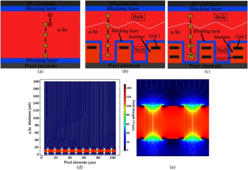
Detector designs have also produced substantial improvements in temporal performance of a-Se sensors. The multiwell solid-state detector (MWSD),33 shown in Fig. 1(b), successfully demonstrated unipolar time differential (UTD) charge sensing, whereby the signal rise time is only dependent on the drift of free holes through a narrow sensing region of the detector, significantly improving the temporal response compared with a conventional transit time-limited planar a-Se detector [Fig. 1(a)]. However, the MWSD design was not optimized for operation at avalanche fields and suffered from high dark current due to charge injection.
Fig. 1.
Cross-section schematic of (a) planar, (b) MWSD, and (c) SWAD detector structures, (d) COMSOL field simulation for SWAD, and (e) close up of SWAD well region, showing the field-shaping effect and localized high field within the a-Se filled wells.
1.3. Field-Shaping Multiwell Avalanche Detector Structure
Direct conversion a-Se flat panel detectors with separate interaction and avalanche gain regions have previously been proposed34 and theoretically analyzed.35 The field-shaping multiwell avalanche detector (SWAD),36 shown in Fig. 1(c), is designed to utilize both avalanche multiplication and UTD charge sensing to overcome the inherent limitations of a-Se. SWAD is a direct conversion detector composed of two distinct regions: (1) a thick a-Se (bulk) layer for high x-ray detection efficiency and (2) a thin (well) sensing region, consisting of a plurality of wells deposited over the readout electronics. The well sidewalls are formed by pillars made of insulating material with two grid electrodes embedded inside. The electric field lines above the pillars bend when the grid electrodes are biased, creating a field-shaping effect that guides carriers into the a-Se filled wells of the sensing region. The electric field within the a-Se filled wells can be tuned to create a localized high field for avalanche multiplication between the two embedded electrodes while maintaining a low field through the bulk region and just above the readout electronics [Figs. 1(d) and 1(e)]. Additionally, grid 2 acts as a Frisch grid,37 electrostatically shielding the pixel electrode from sensing any charge carriers drifting in the bulk region, resulting in a strong near field effect where the collected signal rapidly increases as drifting carriers enter the wells and undergo avalanche multiplication. The common high-voltage electrode in SWAD is biased positively, such that only the faster carriers (holes, in a-Se) are collected in the sensing region. Successful UTD charge sensing in SWAD would produce similar improvements in temporal resolution to that achieved by the MWSD discussed above. The bulk region thickness () is an order of magnitude larger than the well-sensing region (), reducing the probability of x-ray absorption within the sensing region, minimizing the effect of depth-dependent variation in avalanche gain.38 Recently, we demonstrated the first UTD charge sensing time-of-flight measurement with a SWAD prototype sample.39 We are, currently, optimizing our pixel design for stable operation at the high fields required for avalanche gain.
2. Methods
2.1. Detector Description
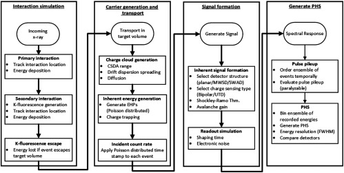
In this work, a probability-based numerical simulation was developed in MATLAB (version 2017b, MathWorks, Inc. Natick, Massachusetts) to model the charge generation, transport, and signal collection processes of three different a-Se detector configurations. Specifically the MWSD, SWAD, and conventional planar detector configurations are modeled. Signal generation for both the bipolar sensing of conventional planar a-Se detectors and the UTD charge sensing of SWAD and MWSD were considered in our model. The simulation flow can be divided into four stages (Fig. 2): (1) probability-based simulation of x-ray interactions within a-Se, (2) carrier generation and transport within the target volume, (3) signal formation, and (4) generation of pulse height spectra (PHS).
Fig. 2.
General overview of simulation flow incorporating x-ray interactions, carrier generation and transport, signal formation, and generation of PHS.
The parameters used to simulate the spectral response of each detector configuration are shown in Table 2. Configuration 1 consists of -thick planar a-Se structure, matching the parameters used in the experimentally measured PHS of a-Se by Blevis et al.40 Detector configuration 2 (MWSD) utilized UTD charge sensing only, and configuration 3 (SWAD) utilized UTD charge sensing with avalanche gain. Detector configurations 2 and 3 were considered to have identical structural dimensions, consisting of a (1) thick a-Se bulk interaction region and (2) a multiwell sensing region (with pillar height) over the pixel electrode. Two different geometries were considered for detector configurations 2 and 3: (1) utilizing a bulk region, for comparison with the planar detector used by Blevis et al.40 and (2) using a thicker bulk region, matching the geometry used in current a-Se AMFPI.27 The assumption of low incident count-rate and large pixel size () was made to investigate the inherent energy resolution of each detector configuration modeled.
Table 2.
Simulated detector configurations and relevant parameters.
| Detector configuration | Configuration 1 planar(Bipolar) | Configuration 2 MWSD (UTD only) | Configuration 3 SWAD (UTD + Av. gain) |
|---|---|---|---|
| Incident energy (keV) | 59.5 | 59.5/30 | 59.5/30 |
| Film thickness () | 150 | 150/200 | 150/200 |
| Applied field () | 20 | 20/10 | 20/10 |
| Shaping time () | 32 | 2 | 2 |
| Pixel size (mm) | — | 1 | 1 |
| Incident count-rate (cps) | 100 | 100 | 100 |
| Sensing type | Bipolar | UTD | UTD |
| Avalanche gain () | No | No | Yes () |
2.2. Simulation of x-ray Interactions
The spectral response of each detector configuration was simulated using monoenergetic x-ray sources at two different energies: (1) 59.5 keV, matching the conditions of the filtered Americium-241 () source used in the experimental measurement by Blevis et al.40 and (2) 30 keV, representing the average energy of a typical polychromatic spectra used in mammography. A low incident count-rate of 100 cps was used for each energy to minimize the effect of pulse pileup and match experimental conditions used by Blevis et al.40 The 59.5 keV source used by Blevis is higher than the typical energies used for dual-energy contrast-enhanced breast imaging tasks,41 and quantum detection efficiency of a-Se at 59.5 keV for is poor, [Fig. 3(a)]. Only photoelectric interactions were considered in our model, as these are the dominant interactions in a-Se at the two energies used, with probability of occurrence at 59.5 keV [Fig. 3(b)] and -fluorescence yield of . -fluorescence emissions are either or with energies of 11.2 and 12.5 keV, respectively, and corresponding yields of 86.2% and 13.8%. Due to the low energy of -fluorescence emissions, -shell interactions were not considered. To simulate the planar geometry (with incident photons confined to the center of collection electrode) used by Blevis et al,40 all primary interactions were centered within the target volume to minimize lateral escape of -fluorescence emissions.
Fig. 3.
(a) Quantum detection efficiency of a-Se as a function of film thickness, (b) normalized interaction cross-section for a-Se (adapted from NIST XCOM database), (c) relevant interaction scenarios in target volume (1) photoelectric absorption without -fluorescence emission, (2) photoelectric absorption with reabsorbed -fluorescence emission, and (3) energy loss due to -fluorescence emission escape.
In general, there are three scenarios of energy deposition that can result from photoelectric absorption occurring within the target volume of a-Se [Fig. 3(c)]: (1) photoelectric interaction occurs without -fluorescence emission and only a single charge cloud is formed, (2) -fluorescence emission is reabsorbed within the target volume, and (3) -fluorescence emission escapes the target volume. In cases (1) and (2), the entire energy of the incident x-ray photon is absorbed within the target a-Se volume; however, in case (2), the deposited energy is split between two spatially separated charge clouds. In case (3), the fluorescence energy is lost from the target volume, resulting in a reduction in the collected signal. Charge sharing from neighboring pixels was not included. X-ray interactions occurring within the well regions of configurations 2 and 3 were not considered.
2.3. Carrier Generation and Transport
The position and energy deposition of each primary photoelectric interaction and -fluorescence reabsorption within the a-Se target volume was tracked. The number of generated EHPs from each interaction is considered to be a Poisson distributed random variable centered about the mean signal generated. The total-root-mean-squared (RMS) spatial spreading of a charge cloud () generated in a-Se is determined by two factors: (1) the initial charge cloud size, determined by the photoelectron range () and (2) carrier diffusion during drift (). It is given as follows:
| (1) |
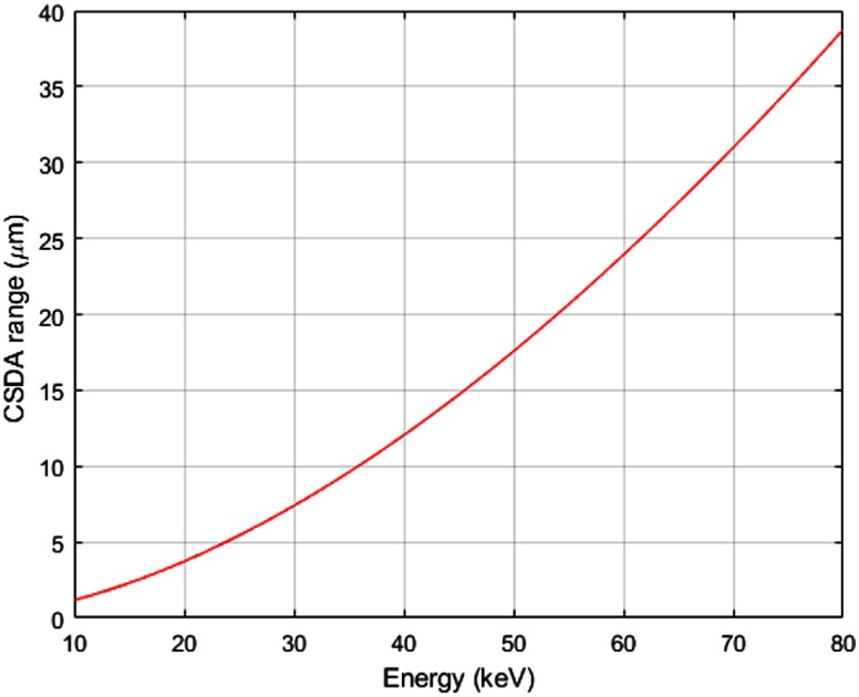
The primary photoelectron range and fluorescence photoelectron range were estimated by the continuous-slowing-down-approximation (CSDA), as shown in Fig. 4, with values taken from the NIST ESTAR database. For configuration 1, electron trapping during charge transport was considered, following the framework developed by Kabir and Kasap.42 Each incident x-ray was tagged with a Poisson distributed time stamp with a mean equal to the incident count-rate, to take into account pulse pileup effects during the signal generation step of the model.
Fig. 4.
CSDA range for electrons in selenium as a function of energy. CSDA ranges were taken from the NIST ESTAR database.
2.4. Signal Formation
2.4.1. Induced current
The signal sensed by the pixel electrodes () can be evaluated by the Shockley–Ramo theorem,43,44 expressed as follows:
| (2) |
where is the electronic charge, is the weighting potential, is the carrier mobility, and is time. Furthermore, the induced current on the collecting pixel is given by the derivative of Eq. (2):
| (3) |
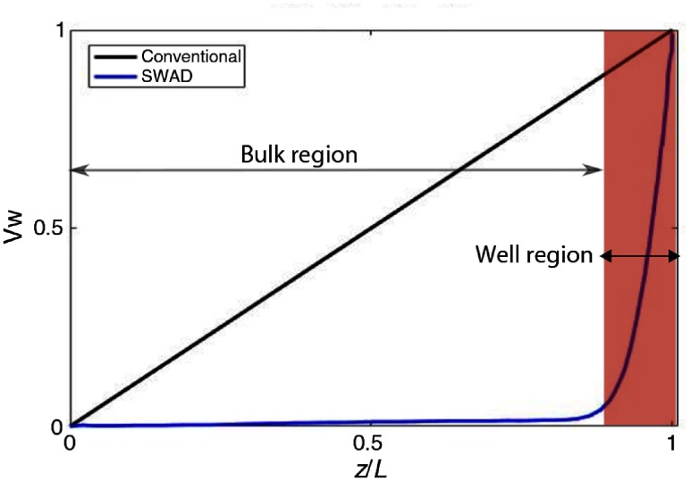
The distributions of as a function of depth within the bulk are shown in Fig. 5 for planar detectors and SWAD with UTD charge sensing. The for detector configurations 2 and 3 were considered to be identical.
Fig. 5.
Comparison of weighting potential distribution for a conventional planar detector (black) and SWAD (blue).
2.4.2. Bipolar planar sensing
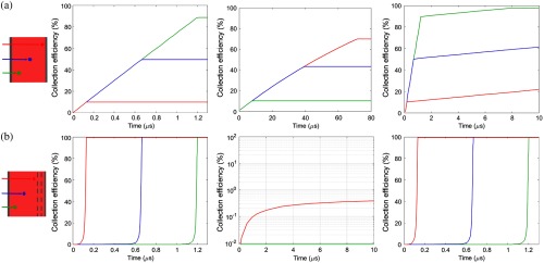
For planar detectors, (Fig. 6, top row), a-Se is sandwiched between two contacts: (1) a common high-voltage electrode, biased at a constant potential to establish a uniform electric field across the a-Se and (2) a collecting electrode that is biased to zero potential and connected to the readout circuitry. Under the assumption that the pixel electrode size is much larger than the photoconductor thickness, the weighting potential of the planar detector is zero at the common high-voltage electrode and increases linearly to one at the collecting electrode. This distribution means that the collector is sensitive to real-time transport of both carriers in the bulk, resulting in a photoresponse that is limited by the transit-time of the carrier drift across the photoconductor. The transit-time-limited response of the planar configuration results in a signal collection whose magnitude is depth dependent, limited primarily by the slower secondary carriers (electrons). Interactions occurring deeper in the a-Se and closer to the collecting pixel electrode (Fig. 6 top row, red lines) need a significantly longer collection time to account for the long electron drift and ensure complete charge compared with interactions occurring further away from the collecting electrode (green curves, Fig. 6 top row), whose collection time is primarily dependent on the transit of faster carriers (holes).
Fig. 6.
Comparison of (a) charge collection efficiency for planar and (b) SWAD as a function of drift time for (left column) holes, (middle column) electrons, and (right column) total signal for three different interaction depths (1) , (2) (midpoint), and (3) in a-Se bulk [adapted from Goldan et al. (Ref. 33)].
2.4.3. Unipolar time differential sensing
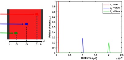
In UTD sensing, (Fig. 6, bottom row), the embedded grid electrodes result in a distribution, which is essentially zero throughout the bulk and then sharply increases in the sensing well region due to the strong near-field effect established by the electrostatic shielding37 of the top grid electrode. These designs result in substantially improved signal rise times compared with conventional planar a-Se detectors, as the pixel electrode is insensitive to charge motion in the bulk, and when properly biased, only the signal from the faster carriers (holes) drifting into the well region is sensed. Fundamentally, the rise time of the integrated signal is only limited by the transit-time required for holes of a generated charge cloud to drift through the well region (33). However, depending on the depth of interaction in the bulk and the subsequent drift distance needed before reaching the well region, carrier diffusion could cause further broadening of the charge cloud (Fig. 7). In this work, we assumed idealized nondispersive Gaussian transport within the a-Se bulk for each detector configuration.45,46 Following this assumption, the drift spreading () and mean position () of the charge cloud obey the time dependencies of and , yielding the relationship:47,48
| (4) |
Fig. 7.
Spread of UTD pulses due to Gaussian dispersion of holes as a function of drift distance for three interactions of different depths within a-Se bulk: (red), (blue), and (green) above well-sensing region. Each pulse is centered about the drift time needed by the charge cloud to travel from absorption depth to sensing electrode.
Following from Eq. (4), the signal rise time for UTD charge sensing is also limited by the spatial spreading of the charge cloud during drift, prior to entering the well region.33
2.4.4. Signal sensing circuitry response
For each detector configuration, the current induced by an absorbed x-ray was integrated over a fixed time interval (i.e., shaping time). At the end of the shaping time, the amplitude of the recorded pulse was considered to be the collected charge signal. For configuration 1, a shaping time of was assumed, matching the experimental conditions of Blevis et al.40 For configurations 2 and 3, with UTD charge sensing, a shaping time of was used. The shaping time of , equal to transit time of holes across bulk at , was chosen to ensure complete collection of charge in the case of two spatially separated charge clouds resulting from the reabsorption of -fluorescence within the same target volume.39 The total electronic noise for configuration 1 () was assumed to be , matching the measured noise from Blevis et al.40 In general, the total noise () contributing to each collected signal from an x-ray interaction within a-Se is given as follows:
| (5) |
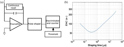
where is the shot noise associated with EHP generation, is the noise due to the dark current of the detector configuration, and is the noise associated with the readout electronics that complete the signal processing. In modern PCDs, arrays of pixelated elements are connected to application-specific integrated circuits (ASICs) consisting of several parallel channels, each containing multiple comparators and counters for pulse height analysis and energy binning. A generalized schematic of an individual channel for a typical photon counting ASIC is shown in Fig. 8(a). Several different photon counting ASICs for medical imaging applications have been developed and characterized at clinically relevant energies using crystalline semiconductors;49 however, these ASICs use faster shaping times than what would be needed for an a-Se. We followed the photon counting pixel design by Goldan et al.50,51 for a-Se sensors with low dark current (), and the simulated input-referred equivalent noise charge (ENC) is shown in Fig. 8(b) as a function of shaping time. It provides the lowest ENC with a shaping time of 200 to 300 ns, which is relevant for configurations 2 and 3, respectively. Following this design assumption, the total electronic noise for detector configurations 2 () with a shaping time was estimated to be . Electronic noise was not considered for detector configuration 3, assuming the amplification of the signal from avalanche gain would overcome the effects of electronic noise.
Fig. 8.
(a) Generalized block schematic of a single channel for a typical photon counting ASIC and (b) ENC as a function of shaping time adapted from photon counting pixel architecture developed by Goldan et al. (Ref. 50).
2.5. Pulse Height Spectra Generation
For each detector configuration, the ensemble of integrated signals was ordered temporally by their time stamp, and any overlap in the recorded waveforms represented pulse pileup. Each detector configuration was modeled as a paralyzable system. The PHS was generated by binning the ensemble of integrated charge from an entire simulation run into a histogram with 0.5-keV resolution. No energy thresholds were applied during the binning process. The energy resolution of each detector was determined by the full-width-at-half-maximum (FWHM) of the primary photo-peak. The PHS and energy resolution of each detector configuration were compared.
3. Results and Discussion
3.1. Validation of Simulation Using Planar Structure
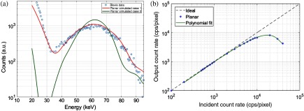
The simulated PHS for configuration 1 is shown in Fig. 9(a). It was generated using 50,000 59.5-keV photons following the parameters summarized in Table 2. Plotted in the same figure are the measured PHS of the planar detector by Blevis et al.40 The simulated results show excellent agreement with the adapted experimental data. The planar detector was found to have an energy resolution of . The broad spectral width can be attributed to incomplete charge collection due to the lower mobility electrons and increased dark current shot noise due to high charge injection at the high fields () used in the measurements. Planar a-Se employing lower dark current with modern blocking layers results in a significant reduction of ENC (500 to ), leading to an energy resolution of at a count-rate of 100 cps. The slow carrier mobility still necessitates a shaping time of , which limits the count-rate linearity of the planar geometry. As shown in Fig. 9(b), a linear response, i.e., with loss due to pulse pileup, is only held up to . The low count-rate and low-energy resolution limit the capability of planar a-Se to accurately resolve single photons under clinical settings.
Fig. 9.
(a) Comparison of adapted experimental data from Blevis et al. (see Ref. 40), simulated planar PHS results under Blevis conditions and with reduced ENC values. (b) Count-rate linearity planar a-Se with planar Se, shaping time, and , exposed to 59.5-keV x-rays.
3.2. Comparison of Energy Resolution
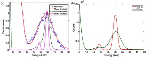
The simulated PHS for each detector configuration using 50,000 incident 59.5 keV x-rays and the measured PHS adapted from Blevis et al.40 are compared in Fig. 10(a). A significant improvement in energy resolution was found for the MWSD, with , compared with the of the planar detector. This enhancement can be attributed to the complete collection of charge and reduced electronic noise of the MWSD. For the MWSD, the extra broadening of the PHS is primarily due to -fluorescence escape. For SWAD, the energy resolution continued to improve (), owing to the signal amplification by avalanche gain prior to readout. As a result, the -fluorescence escape-peak became resolvable from the primary photopeak. The simulated PHS for the MWSD and SWAD configurations is compared [Fig. 10(b)] for a 30-keV monoenergetic source. At this energy, the SWAD structure was found to have a significantly improved energy resolution () compared to the MWSD (). Similar to the 59.5-keV case, the signal amplification from avalanche gain significantly improved the SNR for SWAD, resulting in a boost in energy resolution. As a result, the -fluorescence escape peak became resolvable from the primary photopeak.
Fig. 10.
(a) Comparison experimentally measured PHS adapted from Blevis et al. (Ref. 40), and simulated PHS of each detector configuration with 59.5-keV incident energy. (b) Comparison of simulated PHS for MWSD and SWAD detector structure with 30 keV incident energy.
3.3. Investigation into Field-Shaping Multiwell Avalanche Detector Performance
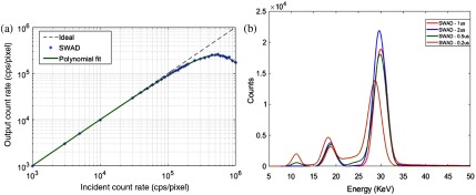
In the previously discussed results shown in Sec. 3.2, a shaping time of , which is equal to the transit-time of holes across the a-Se bulk of SWAD, was chosen to ensure complete charge collection of spatially separated charge clouds resulting from K-fluorescence reabsorption. The count-rate linearity of SWAD with a bulk layer and 59.5-keV exposure is shown in Fig. 11(a). SWAD has a linear response, i.e., with loss due to pulse pileup, for input count-rates approaching , performing substantially better than the planar structure. This count-rate is sufficient for the x-ray flux typically used in DBT.39 However, a shaping time of is significantly larger than typical shaping times used in current ASICs for PCDs.49 For SWAD to be a potential candidate for higher flux applications, a faster shaping time may be necessary to improve the count-rate linearity. The PHS for SWAD with different shaping times is shown in Fig. 11(b). The change in the PHS is negligible until shaping times fall below . For shaping times below , the charge clouds of reabsorbed -fluorescence photons are collected and registered as separate events, which is evidenced by a -fluorescence peak in the PHS. Additionally, the incomplete collection shifts the primary photopeak and degrades the energy resolution.
Fig. 11.
(a) Count-rate linearity of SWAD with a-Se bulk, shaping time, and pixel at 59.5 keV, and (b) comparison of SWAD PHS for 2-, 1-, 0.5-, and shaping times.
3.4. Limitations of the Present Study
A large pixel size () was chosen to match the experimental conditions of previously published PHS measurements and compare the inherent energy resolution and count rate linearity of three different detector configurations. For the small pixel sizes needed in mammography (), the PHS may be degraded by spatial charge sharing effects52 caused by -fluorescence reabsorption and charge cloud spreading, which were omitted in this work. However, these effects were investigated separately in our previous work for using pixel sizes relevant for mammography (100 and ).52 With regard to charge sharing due to -fluorescence reabsorption into neighboring pixels, the lower -fluorescence energy of a-Se leads to less effect compared with higher materials. With regard to charge sharing due to charge cloud spreading across pixel boundaries, a-Se detectors have an inherent advantage compared with CdTe/CZT detectors due to their relatively low carrier mobility and high electric field, which result in negligible lateral expansion of the charge cloud during drift. This property has been shown experimentally with ultrahigh-resolution a-Se x-ray detectors.53–55 Additionally, for smaller pixel sizes there will be some improvement in charge collection from the “small pixel effect.”56 However, due to the limited thickness of a-Se used for breast imaging (), the “small pixel effect” is not sufficient to completely overcome limitations resulting from the slow transit-time of electrons.57 Our future work will incorporate these effects for a more complete analysis of energy resolution and count rate linearity for small pixels.
4. Conclusions
In this work, we developed a comprehensive probability-based numerical simulation to model the detector response and generate PHS for three different a-Se detector configurations. Our model showed excellent agreement with the experimental measurements of Blevis et al.,40 confirming the validity of our simulation. The impact of UTD charge sensing and avalanche gain was investigated for two different cases (1) simulating the detector performance using a filtered source (59.5 keV), identical to the experimental setup used by Blevis et al.40 and (2) using a low count-rate, 30-keV source with a detector geometry matching those used in modern a-Se-based AMFPI for digital mammography. In both cases, UTD charge sensing and avalanche gain provided significant improvements in energy resolution compared with conventional planar detector structures. The combination of avalanche gain and UTD charge sensing in the SWAD detector had the best energy resolution in each case. The count-rate capabilities of SWAD were found to be substantially higher than that of the planar configuration. The SWAD design with fast UTD charge sensing achieved a linear response for incident count-rates approaching , showing its promise for clinical applications such as DBT. The SWAD structure was found to have comparable energy resolution to modern CdTe-based PCDs58 exposed to filtered sources. Future work will involve extending our current charge transport model to investigate the performance of SWAD with smaller pixel sizes and high incident count-rates.
Acknowledgments
We gratefully acknowledge financial support from the National Institutes of Health (R01 EB026267, R21 EB019526, R21 EB024849, and R21 EB025300). The authors thank Adrian Howansky, Hailiang Huang, Drs. James Scheuermann, and Anthony Lubinsky for their helpful suggestions and discussions. This work was partially published in a SPIE medical imaging conference proceedings paper, “Photon counting performance of amorphous selenium and its dependence on detector structure” (2018). This work expands the initial results to include a comparison of PHS with clinically relevant settings, SWAD performance as a function of shaping time, and count-rate linearity of SWAD and planar sensors.
Biographies
Jann Stavro received his MS degree in biomedical engineering from Stony Brook University in 2016, and his BS degree in physics and applied mathematics from the University of California, Davis in 2011. Currently, he is a PhD student at Stony Brook University. His current research interests include development of energy-resolving photon counting detectors, fabrication of novel amorphous selenium-based sensors, and digital breast imaging applications. He is a member of SPIE.
Amir H. Goldan is a research assistant professor at Stony Brook University. He received his PhD in electrical engineering from the University of Waterloo in 2012. He has coinvented, developed, and optimized several direct and indirect detector technologies, and introduced the novel concept of unipolar time-differential charge sensing in amorphous solids. His current research interests include investigating the molecular structure of amorphous selenium and developing avalanche selenium detectors for time-of-flight PET and photon counting applications.
Wei Zhao is a professor of radiology at Stony Brook University. She received her PhD in medical biophysics from the University of Toronto in 1997. Her current research interests include the optimization of imaging system geometry and flat-panel detector performance for DBT and dual-energy contrast-enhanced imaging applications, as well as the development of a-Se-based indirect flat panel detectors with avalanche gain for low-dose imaging applications. She is a member of SPIE.
Disclosures
The authors have no conflicts of interest to disclose.
References
- 1.Taguchi K., Iwanczyk J. S., “Vision 20/20: single photon counting x‐ray detectors in medical imaging,” Med. Phys. 40(10), 100901 (2013). 10.1118/1.4820371 [DOI] [PMC free article] [PubMed] [Google Scholar]
- 2.Swank R. K., “Absorption and noise in x‐ray phosphors,” J. Appl. Phys. 44(9), 4199–4203 (1973). 10.1063/1.1662918 [DOI] [Google Scholar]
- 3.Tapiovaara M. J., Wagner R., “SNR and DQE analysis of broad spectrum x-ray imaging,” Phys. Med. Biol. 30(6), 519–529 (1985). 10.1088/0031-9155/30/6/002 [DOI] [Google Scholar]
- 4.Schmidt T. G., “Optimal ‘image‐based’ weighting for energy‐resolved CT,” Med. Phys. 36(7), 3018–3027 (2009). 10.1118/1.3148535 [DOI] [PubMed] [Google Scholar]
- 5.Fredenberg E., “Spectral and dual-energy X-ray imaging for medical applications,” Nucl. Instrum. Methods Phys. Res., Sect. A 878, 74–87 (2018). 10.1016/j.nima.2017.07.044 [DOI] [Google Scholar]
- 6.Bornefalk H., et al. , “Single-shot dual-energy subtraction mammography with electronic spectrum splitting: feasibility,” Eur. J. Radiol. 60(2), 275–278 (2006). 10.1016/j.ejrad.2006.08.004 [DOI] [PubMed] [Google Scholar]
- 7.Johansson H., et al. , “Breast‐density measurement using photon‐counting spectral mammography,” Med. Phys. 44(7), 3579–3593 (2017). 10.1002/mp.2017.44.issue-7 [DOI] [PMC free article] [PubMed] [Google Scholar]
- 8.Ghammraoui B., Glick S. J., “Investigating the feasibility of classifying breast microcalcifications using photon‐counting spectral mammography: a simulation study,” Med. Phys. 44(6), 2304–2311 (2017). 10.1002/mp.2017.44.issue-6 [DOI] [PubMed] [Google Scholar]
- 9.Erhard K., et al. , “Characterization of cystic lesions by spectral mammography: results of a clinical pilot study,” Invest. Radiol. 51(5), 340–347 (2016). 10.1097/RLI.0000000000000246 [DOI] [PubMed] [Google Scholar]
- 10.Åslund M., et al. , “Physical characterization of a scanning photon counting digital mammography system based on Si‐strip detectors,” Med. Phys. 34(6), 1918–1925 (2007). 10.1118/1.2731032 [DOI] [PubMed] [Google Scholar]
- 11.Fredenberg E., et al. , “A photon-counting detector for dual-energy breast tomosynthesis,” Proc. SPIE 7258, 72581J (2009). 10.1117/12.813037 [DOI] [Google Scholar]
- 12.Weigel S., et al. , “Digital mammography screening with photon-counting technique: can a high diagnostic performance be realized at low mean glandular dose?” Radiology 271(2), 345–355 (2014). 10.1148/radiol.13131181 [DOI] [PubMed] [Google Scholar]
- 13.Fredenberg E., et al. , “Energy resolution of a photon-counting silicon strip detector,” Nucl. Instrum. Methods Phys. Res., Sect. A 613(1), 156–162 (2010). 10.1016/j.nima.2009.10.152 [DOI] [Google Scholar]
- 14.Barber W. C., et al. , “Fast photon counting CdTe detectors for diagnostic clinical CT: dynamic range, stability, and temporal response,” Proc. SPIE 7622, 76221E (2010). 10.1117/12.844669 [DOI] [Google Scholar]
- 15.Iwanczyk J. S., et al. , “Photon counting energy dispersive detector arrays for x-ray imaging,” IEEE Trans. Nucl. Sci. 56(3), 535–542 (2009). 10.1109/TNS.2009.2013709 [DOI] [PMC free article] [PubMed] [Google Scholar]
- 16.Lundqvist M., et al. , “Computer simulations and performance measurements on a silicon strip detector for edge-on imaging,” IEEE Trans. Nucl. Sci. 47(4), 1487–1492 (2000). 10.1109/23.873002 [DOI] [Google Scholar]
- 17.Zambon P., et al. , “Spectral response characterization of CdTe sensors of different pixel size with the IBEX ASIC,” Nucl. Instrum. Methods Phys. Res., Sect. A 892, 106–113 (2018). 10.1016/j.nima.2018.03.006 [DOI] [Google Scholar]
- 18.Yin S., et al. , “Direct conversion CdZnTe and CdTe detectors for digital mammography,” IEEE Trans. Nucl. Sci. 49(1), 176–181 (2002). 10.1109/TNS.2002.998748 [DOI] [Google Scholar]
- 19.Bellazzini R., et al. , “Chromatic X-ray imaging with a fine pitch CdTe sensor coupled to a large area photon counting pixel ASIC,” J. Instrum. 8(02), C02028 (2013). 10.1088/1748-0221/8/02/C02028 [DOI] [Google Scholar]
- 20.Xu C., Danielsson M., Bornefalk H., “Evaluation of energy loss and charge sharing in cadmium telluride detectors for photon-counting computed tomography,” IEEE Trans. Nucl. Sci. 58(3), 614–625 (2011). 10.1109/TNS.2011.2122267 [DOI] [Google Scholar]
- 21.Pellegrini G., et al. , “Performance limits of a 55-/spl mu/m pixel CdTe detector,” IEEE Trans. Nucl. Sci. 53(1), 361–366 (2006). 10.1109/TNS.2006.869843 [DOI] [Google Scholar]
- 22.Shikhaliev P. M., Fritz S. G., Chapman J. W., “Photon counting multienergy x‐ray imaging: Effect of the characteristic X rays on detector performance,” Med. Phys. 36(11), 5107–5119 (2009). 10.1118/1.3245875 [DOI] [PubMed] [Google Scholar]
- 23.Bolotnikov A., et al. , “Factors limiting the performance of CdZnTe detectors,” IEEE Trans. Nucl. Sci. 52(3), 589–598 (2005). 10.1109/TNS.2005.851419 [DOI] [Google Scholar]
- 24.Szeles C., et al. , “CdZnTe semiconductor detectors for spectroscopic X-ray imaging,” IEEE Trans. Nucl. Sci. 55(1), 572–582 (2008). 10.1109/TNS.2007.914034 [DOI] [Google Scholar]
- 25.Yu Z., et al. , “Evaluation of conventional imaging performance in a research whole-body CT system with a photon-counting detector array,” Phys. Med. Biol. 61(4), 1572–1595 (2016). 10.1088/0031-9155/61/4/1572 [DOI] [PMC free article] [PubMed] [Google Scholar]
- 26.Kasap S., et al. , “Amorphous selenium and its alloys from early xeroradiography to high resolution X‐ray image detectors and ultrasensitive imaging tubes,” Phys. Status Solidi (B) 246(8), 1794–1805 (2009). 10.1002/pssb.v246:8 [DOI] [Google Scholar]
- 27.Sechopoulos I., “A review of breast tomosynthesis. Part I. The image acquisition process,” Med. Phys. 40(1), 014301 (2013). 10.1118/1.4770279 [DOI] [PMC free article] [PubMed] [Google Scholar]
- 28.Tanioka K., et al. , “An avalanche-mode amorphous selenium photoconductive layer for use as a camera tube target,” IEEE Electron Device Lett. 8(9), 392–394 (1987). 10.1109/EDL.1987.26671 [DOI] [Google Scholar]
- 29.Bubon O., et al. , “Electroded avalanche amorphous selenium (a-Se) photosensor,” Curr. Appl. Phys. 12(3), 983–988 (2012). 10.1016/j.cap.2011.12.023 [DOI] [PMC free article] [PubMed] [Google Scholar]
- 30.Takiguchi Y., et al. , “A CMOS imager hybridized to an avalanche multiplied film,” IEEE Trans. Electron Devices 44(10), 1783–1788 (1997). 10.1109/16.628837 [DOI] [Google Scholar]
- 31.Scheuermann J. R., et al. , “Development of solid‐state avalanche amorphous selenium for medical imaging,” Med. Phys. 42(3), 1223–1226 (2015). 10.1118/1.4907971 [DOI] [PMC free article] [PubMed] [Google Scholar]
- 32.Scheuermann J. R., et al. , “Toward scintillator high‐gain avalanche rushing photoconductor active matrix flat panel imager (SHARP‐AMFPI): initial fabrication and characterization,” Med. Phys. 45(2), 794–802 (2018). 10.1002/mp.12693 [DOI] [PMC free article] [PubMed] [Google Scholar]
- 33.Goldan A., et al. , “Unipolar time-differential charge sensing in non-dispersive amorphous solids,” J. Appl. Phys. 113(22), 224502 (2013). 10.1063/1.4807292 [DOI] [Google Scholar]
- 34.Lee D. L., “Selenium detector with a grid for selenium charge gain,” Proc. SPIE 5745, 216–223 (2005). 10.1117/12.594623 [DOI] [Google Scholar]
- 35.Wronski M., Rowlands J., “Direct‐conversion flat‐panel imager with avalanche gain: Feasibility investigation for HARP‐AMFPI,” Med. Phys. 35(12), 5207–5218 (2008). 10.1118/1.3002314 [DOI] [PMC free article] [PubMed] [Google Scholar]
- 36.Goldan A., Zhao W., “A field‐shaping multi‐well avalanche detector for direct conversion amorphous selenium,” Med. Phys. 40(1), 010702 (2013). 10.1118/1.4769110 [DOI] [PMC free article] [PubMed] [Google Scholar]
- 37.Frisch O., “British atomic energy report,” BR-49, 65 (1944).
- 38.Lui B. J., et al. , “X‐ray imaging with amorphous selenium: pulse height measurements of avalanche gain fluctuations,” Med. Phys. 33(9), 3183–3192 (2006). 10.1118/1.2335491 [DOI] [PubMed] [Google Scholar]
- 39.Stavro J., et al. , “SWAD: transient conductivity and pulse-height spectrum,” Proc. SPIE 10132, 1013208 (2017). 10.1117/12.2255733 [DOI] [Google Scholar]
- 40.Blevis I., Hunt D., Rowlands J., “Measurement of x-ray photogeneration in amorphous selenium,” J. Appl. Phys. 85(11), 7958–7963 (1999). 10.1063/1.370615 [DOI] [Google Scholar]
- 41.Hu Y.-H., Zhao W., “A 3D linear system model for the optimization of dual-energy contrast-enhanced digital breast tomosynthesis,” Proc. SPIE 7961, 79611C (2011). 10.1117/12.878134 [DOI] [Google Scholar]
- 42.Kabir M. Z., Kasap S., “Sensitivity of x-ray photoconductors: charge trapping and absorption-limited universal sensitivity curves,” J. Vac. Sci. Technol., B 20(3), 1082–1086 (2002). 10.1116/1.1460900 [DOI] [Google Scholar]
- 43.Shockley W., “Currents to conductors induced by a moving point charge,” J. Appl. Phys. 9(10), 635–636 (1938). 10.1063/1.1710367 [DOI] [Google Scholar]
- 44.Ramo S., “Currents induced by electron motion,” Proc. IRE 27(9), 584–585 (1939). 10.1109/JRPROC.1939.228757 [DOI] [Google Scholar]
- 45.Kasap S., Brinkhurst D., Haugen C., “Modelling of photoinduced discharge of photoreceptors under pulsed photoexcitation: small and large signal xerographic time-of-flight analysis,” J. Phys. D: Appl. Phys. 33(4), 449–463 (2000). 10.1088/0022-3727/33/4/320 [DOI] [Google Scholar]
- 46.Polischuk B., Kasap S., Baillie A., “Study of photogenerated charge carrier dispersion in chlorinated a‐Se: 0.3% As by the interrupted field time‐of‐flight technique,” Appl. Phys. Lett. 63(2), 183–185 (1993). 10.1063/1.110393 [DOI] [Google Scholar]
- 47.Scher H., “Anomalous transit-time dispersion in amorphous solids,” Phys. Rev. B 12, 2455–2477 (1975). 10.1103/PhysRevB.12.2455 [DOI] [Google Scholar]
- 48.Pfister G., Scher H., “Dispersive (non-Gaussian) transient transport in disordered solids,” Adv. Phys. 27(5), 747–798 (1978). 10.1080/00018737800101474 [DOI] [Google Scholar]
- 49.Ballabriga R., et al. , “Review of hybrid pixel detector readout ASICs for spectroscopic X-ray imaging,” J. Instrum. 11(01), P01007 (2016). 10.1088/1748-0221/11/01/P01007 [DOI] [Google Scholar]
- 50.Goldan A. H., et al. , “Photon counting pixel architecture for x-ray and gamma-ray imaging applications,” Proc. SPIE 6510, 65103V (2007). 10.1117/12.710358 [DOI] [Google Scholar]
- 51.Goldan A., et al. , “Photon counting readout pixel array in CMOS technology for on-line gamma-ray imaging of 103 palladium seeds for permanent breast seed implant (PBSI) brachytherapy,” Proc. SPIE 6913, 69130S (2008). 10.1117/12.770766 [DOI] [Google Scholar]
- 52.Stavro J., Goldan A. H., Zhao W., “SWAD: inherent photon counting performance of amorphous selenium multi-well avalanche detector,” Proc. SPIE 9783, 97833Q (2016). 10.1117/12.2217248 [DOI] [Google Scholar]
- 53.Hunter D. M., et al. , “Measured and calculated K‐fluorescence effects on the MTF of an amorphous‐selenium based CCD x‐ray detector,” Med. Phys. 39(2), 608–622 (2012). 10.1118/1.3673957 [DOI] [PubMed] [Google Scholar]
- 54.Scott C., et al. , “High dose efficiency, ultra-high resolution amorphous selenium/CMOS hybrid digital X-ray imager,” in IEEE Int. Electron Devices Meeting (IEDM) (2015). [Google Scholar]
- 55.Oguro T., et al. , “Ultra high resolution digital xeroradiography for x-ray microscopic detector,” Med. Imaging Technol. 7, 279–280 (1989). [Google Scholar]
- 56.Barrett H., Eskin J., Barber H., “Charge transport in arrays of semiconductor gamma-ray detectors,” Phys. Rev. Lett. 75(1), 156–159 (1995). 10.1103/PhysRevLett.75.156 [DOI] [PubMed] [Google Scholar]
- 57.Chen J., et al. , “Feasibility of amorphous selenium based photon counting detectors for digital breast tomosynthesis,” Proc. SPIE 7258, 72581G (2009). 10.1117/12.813361 [DOI] [Google Scholar]
- 58.Steadman R., Herrmann C., Livne A., “ChromAIX2: a large area, high count-rate energy-resolving photon counting ASIC for a spectral CT Prototype,” Nucl. Instrum. Methods Phys. Res., Sect. A 862, 18–24 (2017). 10.1016/j.nima.2017.05.010 [DOI] [Google Scholar]


