

Abstract
Femtosecond laser surface processing is a technology that can be used to functionalize many surfaces, imparting specialized properties such as increased broadband optical absorption or superhydrophilicity/superhydrophobicity. In this study, two unique classes of surface structures, below surface growth (BSG) and above surface growth (ASG) mounds, were formed by femtosecond laser surface processing on amorphous and polycrystalline Ni60Nb40 with two different grain sizes. Cross sectional imaging of these mounds revealed thermal evidence of the unique formation processes for each class of surface structure. BSG mounds formed on all three substrates using the same laser parameters had similar surface morphology. The microstructures in the mounds were unaltered compared with the substrate before laser processing, suggesting their formation was dominated by preferential valley ablation. ASG mounds had similar morphology when formed on the polycrystalline Ni60Nb40 substrates with 100 nm and 2 [H9262]m grain size. However, the ASG mounds had significantly wider diameter and higher peak-to-valley heights when the substrate was amorphous Ni60Nb40. Hydrodynamic melting was primarily responsible for ASG mound formation. On amorphous Ni60Nb40 substrates, the ASG mounds are most likely larger due to lower thermal diffusivity. There was clear difference in growth mechanism of femtosecond laser processed BSG and ASG mounds, and grain size does not appear to be a factor.
Keywords: Femtosecond laser, Ni60Nb40, Microstructure, Laser ablation
1. Introduction
Processing with ultrafast lasers is an emerging technique for the creation of functionalized surfaces through the formation of self-organized, multiscale structures [1–4]. This type of laser processing is applicable for a wide range of materials, including metals [5–9], semiconductors [10,11], polymers [12–14], glass [15,16] and ceramics [17,18].
The resulting micro/nanostructures provide tailored surface properties with many promising applications in diverse fields. One important application is the “hyperdoping” of silicon, where ultrafast laser processing resulted in increased dopant concentration and multiscale surface structures [19,20]. Hyperdoped silicon can be used for increased light absorption of photo-voltaics [17,21,22] and optical sensors [23,24]. Laser processed surfaces can also exhibit special wetting/wicking properties, such as superhydrophobicity or superhydrophilicity[25–27]. Potentials uses include enhanced heat transfer [28–30], self-cleaning surfaces[31], biomedical implants [32,33], drag reduction [34], and chemical sensors [35].
Surface micro/nanostructures formed by femtosecond laser processing on metals feature great diversity in morphology and size[8]. Low laser fluence near the ablation threshold of the target material, forms laser-induced periodic surface structures (LIPSS) and nanoparticle-covered pyramids [6,36–38]. LIPSS are ripples oriented either parallel or perpendicular to the laser polarization, depending on the target material and laser parameters, and have periods with the same order of magnitude as the laser wavelength [8,38,39]. They form after a low number of laser pulses (~10–1000) [2]. After additional laser pulses (2000+) in the same fluence range of LIPSS, NCPs can develop [36–38]. These structures can be as tall as 50 [H9262]m in height, and are covered with a layer of nanoparticles typically more than 2 [H9262]m thick. These start as small (<10 [H9262]m) precursor cones that increase in height, relative to the surrounding valley via preferential laser ablation. These pyramids increase in size by redeposition of nanoparticles produced during the laser ablation process [36,40].
Femtosecond laser surface processing on a metal surface at a laser fluence an order of magnitude higher or more than the ablation threshold can lead to formation of mound-like structures [5,41]. These mounds can reach tens of microns in width and height, and are covered by additional, smaller scale micro/nanostructuring. These mound-like structures are of great research interest because they can be used to produce functionalized metal surfaces that are either superhydrophobic [42] or superhydrophilic [29]. For example, it was demonstrated that such superhydrophilic surfaces can enhance two-phase heat transfer [28,30]. Mounds can be further divided into two distinct classes: below-surface-growth (BSG) and above-surface-growth (ASG) mounds [5,40,43]. BSG mounds are tightly spaced, have low height-to-width aspect ratio (~1:1), and have peaks which are below the original target surface. In contrast, ASG mounds are spaced farther apart, separated by pits, have high aspect ratio (>2:1), and protrude up to several [H9262]m above the original surface. In previous studies by Zuhlke et al. of femtosecond laser surface processing on Ni-based alloys 200/201 showed that BSG mound formation occurred in the fluence range of approximately 1–2 J cm−2 and ASG mounds at approximately 2–3 J cm−2 [5,40,43], as much as two orders of magnitude higher laser fluence than the ablation threshold of Ni (0.05–0.1 J cm−2) [44,45].
2. Theory
BSG and ASG mounds are thought to originate by small precursor ripples, mounds and pits that develop after a low number of laser pulses. For Ni 200/201, this occurs at about <120 pulses for BSG and <30 pulses for ASG mounds [5]. These precursor sites cause a non-uniform distribution of laser energy, leading to the formation processes thought to produce BSG and ASG mounds [5,40].
One of the formation processes associated with mounds is preferential valley ablation. This is the process where the valleys, or low areas of the surface, are ablated more than the peak or top of precursor mounds [5,38,46]. As illustrated in Fig. 1, two phenomena contribute to preferential valley ablation: (a) the higher fluence in the valleys (labelled as “1” on Fig. 1) than on the sides of the mounds due to larger subtended area resulting from increased incident angle (labelled as “2” on Fig. 1), and (b) a portion of the light incident on the sides of the peaks is scattered onto the valleys. BSG mounds on metals are believed to be formed primarily through preferential valley ablation, similar to “spikes” that formed on Si substrates[47].
Fig. 1.
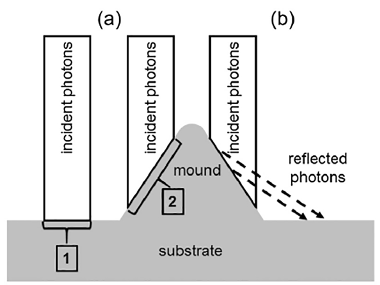
Diagram of the preferential valley ablation mechanism of (a) differences in subtended area and (b) scattered photons.
A second mound formation mechanism is hydrodynamical fluid flow. This is the process where, during ultrafast laser pulse irradiation, the substrate surface melts and the resulting liquid layer flows away from the valleys up the sides of the structures and onto the peaks [48–50]. Resolidification of this layer increases the height of the peaks, and is thought to be a significant part of the ASG mound formation process [5,46]. Fluid flow could be the result of higher laser fluence at valleys versus sides, or could be due to laser-induced shock waves [51,52].
Lastly, redeposition of ablated material can also contribute to mound growth, most likely in the form of smaller, micrometer-sized hemispherical caps that decorate the top of ASG mounds. Redeposition can be described as vapor-liquid-solid growth, where a plume of vaporized metal is solidified and deposited on top of the mounds in the form of nanoparticles [5,38,40].
Currently, there has not been a comprehensive model of femtosecond laser surface processed micro/nanostructures formation due to the complexity of the process. Such a model would have to account for many potential formation mechanisms and multiple types of surface structures. There are several theories developed to explain LIPSS formation on Si substrates [53,54], along with several predictive computer models [49,55]. However, there has not been a fully comprehensive understanding of the formation of larger femtosecond laser processed structures, e.g. NCPs, BSG and ASG mounds, on metals. Knowledge of such growth mechanisms will aid in understanding the physics behind laser-matter interaction, and can improve the performance of functionalized surfaces in applications such as heat transfer and self-cleaning.
3. Materials and methods
It has been proposed that the precursor sites for these femtosecond laser surface processed micro/nanostructures originate at micro/nanoscale defects present in the original metal surface [5,40,56]. Possible initiation sites for mound growth are grain boundaries [56]. The typical grain size for the Ni, stainless steel, and Ti surfaces in previous femtosecond laser processing studies are on the order of one to tens of microns, the same length scale as these mounds [7]. There has been some previous work on grain boundary effects on LIPSS formation [56], but none to our knowledge on these larger-scale surface structures. In this study, the ablation threshold and femtosecond laser surface processing mound formation are compared on three substrates with identical chemical composition, but different crystalline microstructure: two different grain sizes, and one amorphous (i.e. without any grain boundaries).
The alloy utilized in this study was the well-characterized, easy glass-forming Ni60Nb40 [57,58]. Arc-melting and melt spinning formed amorphous Ni60Nb40 ribbons as described in previous published study[46]. Ribbons were sealed in quartz tube under Ar atmosphere after repeated evacuation cycles to prevent oxidation. Then, they were annealed in a tube furnace at 1373 K for either 2 or 20 h to obtain polycrystalline structures with two different grain sizes.
Subsequent polycrystalline Ni60Nb40 microstructures were characterized using SEM and energy dispersive x-ray spectroscopy (EDS) in the FEI Helios NanoLab DualBeam. X-ray diffraction (XRD) using Cu K[H9251] radiation in a Bruker-AXS D8 Discover X-ray Diffractometer provided phase analysis. All XRD samples were mounted on a zero-background holder made from an off-cut Si single crystal. Ribbon surfaces were polished through standard metallurgical procedures, with final polish using 0.05 [H9262]m Al2O3 powder, in preparation for femtosecond laser surface processing. The polished ribbons were cleaned in an ultrasonic bath through successively submerging in acetone, methanol, and deionized water for 20 min each.
Femtosecond laser surface processing was carried out using a Ti:Sapphire femtosecond laser system, Spectra Physics Spitfire as previously described[46]. The laser spot size, which was used to calculate the laser fluence and pulse count, along with ablation threshold, was determined using the method outlined by Liu [59].
All three different substrates, with the three different microstructures, were subject to identical femtosecond laser surface processing parameters to create each type of mound. The laser beam spot diameter was 206 [H9262]m. BSG mounds were produced using 515 laser pulses at a peak fluence of 2.14 J cm−2, with translation speed and pitch of 3 mm s−1 and 15 [H9262]m, respectively. This laser fluence was chosen as it was close to the minimum required for BSG mound formation on Ni60Nb40. The ASG mounds were fabricated using 175 laser pulses with a peak laser fluence of 6.10 J cm−2, with translation speed and pitch of 4.5 mm s−1 and 15 [H9262]m, respectively. The chosen laser fluence was at the high end for ASG mound formation to ensure surface structures that were distinct from BSG mounds. These fluence values for femtosecond laser surface processing mound formation on Ni60Nb40 were found to be about twice that for Ni 200/201 [5]. However, the previous Ni 200/201 mound-formation work was performed with a square top-hat beam profile, while this study utilized a Gaussian beam profile. Due to larger variations in fluence across the Gaussian profile, a higher peak laser fluence is generally required to achieve the same surface structures. The laser pulse counts were chosen for maximum growth of both types of mounds. Evolution of surface structures as a function of laser pulse counts was similar to what was previously used for femtosecond laser processing of Ni 200/201, on which the final, saturated BSG and ASG structures were reached after 600 and 150 pulses, respectively [5].
The underlying microstructure of these BSG and ASG mounds, as revealed by examination of cross-sections, can provide information on their formation mechanisms, such as evidence of thermal events like fluid flow or defects that serve as ablation precursor sites. There have been several previous studies on femtosecond laser surface processing of silicon and metals that utilize cross sections for this purpose [7,40,46,60,61]. SEM imaging and cross sectional milling of the BSG and ASG mounds were performed with the FEI Helios NanoLab 660 DualBeam. This technique is a modification of the TEM “liftout” sample preparation process [62,63]. The target mound was first protected by Pt layers deposited via electron-beam induced deposition (100 nm thick) and ion beam-induced deposition (2 [H9262]m thick). Then, focused ion beam (FIB) milling using Ga+ removed approximately half of the mound and the surrounding material to reveal the resulting cross-section. Imaging was per formed using ion-induced secondary electrons (ISE) at a tilt of 52°.
4. Results
4.1. Ni60Nb40 substrate analysis
Fig. 2(a) shows the XRD scan of the melt-spun Ni60Nb40 ribbons, which revealed an amorphous structure as indicated by the diffuse x-ray diffraction maxima. The XRD patterns of the annealed Ni60Nb40 ribbons were revealed to be polycrystalline, with peaks indexing to two distinct phases: orthorhombic Ni3Nb and rhombohedral Ni6Nb7 (Fig. 2(b) & (c)). These two intermetallic compounds were consistent with what was expected from the equilibrium phase diagram at the Ni60Nb40 composition [64–66]. SEM images (Fig. 3) revealed a two phase structure for ribbons annealed for 2 and 20 h that was consistent with XRD analysis. The average Ni3Nb grain size was approximately 100 nm after the 2 h heat treatment and 2 [H9262]m after the 20 h heat treatment. The individual Ni6Nb7 grains were not evident due to weak channeling contrast between differently-oriented grains. Location-specific EDS spectra were collected by EDAX Octane Silicon Drift Detector (SDD). A semi-quantitative EDS analysis was performed with the EDAX TEAM EDS software. The analysis revealed the composition of the light-colored grains to be 75.9 ± 0.9 at.% Ni and 24.1 ± 0.5 at.% Nb, close to the expected Ni3Nb phase composition. The composition of the darker regions was determined to be 45.7 ± 1.0 at.% Ni and 54.3 ± 1.5 at.% Nb, which correspond to the Ni6Nb7 phase.
Fig. 2.
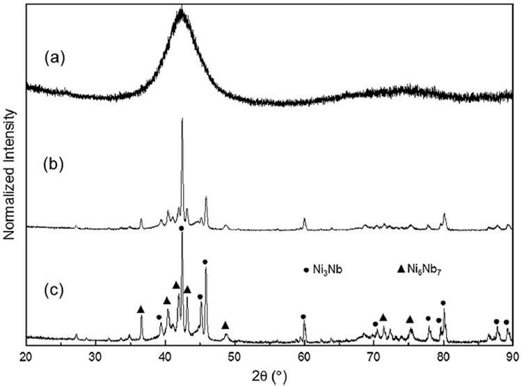
X-ray diffraction patterns of (a) as-solidified Ni60Nb40 ribbons displaying an amorphous structure, and after heat treatment at 1373 K for (b) 2 h and (c) 20 h. Diffraction peaks were indexed to Ni3Nb and Ni6Nb7.
Fig. 3.

SEM images of polycrystalline Ni60Nb40 displaying Ni6Nb7 (dark grey) and Ni3Nb (light grey) phases after annealing at 1373 K for (a) 2 h and (b) 20 h, with average grain sizes of 100 nm and 2 μm, respectively.
4.2. Ablation threshold
Ablation threshold testing was performed with 100 pulses of 50 fs duration from 50 to 700 μJ pulse energy with 50 μJ increments. The Keyence VK-X 3D Laser Scanning Confocal Microscope (3DLSCM) was used to measure ablation crater area and calculate diameter of the equivalent circular area (i.e., 20 μm diameter for 314 μm2 ablated area). Four sets of such ablation spots were analyzed on each of the three substrates. The square of the diameter was plotted against the natural log of laser power and fitted linearly to determine laser spot radius and threshold fluence[59].
The average ablation test results for each form of Ni60Nb40 are displayed in Table 1. There was no statistical difference in the threshold fluence, nor the expected ablation spot size at threshold fluence for the three types of substrates.
Table 1.
Spot radius and threshold fluence of amorphous and polycrystalline Ni60Nb40 with 100 nm and 2 μm average grain sizes.
| Amorphous | Polycrystalline (100nm) |
Polycrystalline (2 μm) |
|
|---|---|---|---|
| Spot radius (μm) | 103.5 ± 1.7 | 103.8 ± 1.4 | 102.4 ± 2.7 |
| Threshold fluence (J cm−2) | 0.100 ± 0.004 | 0.104 ± 0.002 | 0.102 ± 0.07 |
4.3. BSG & ASG mound morphology
Fig. 4 displays SEM images of the BSG and ASG mounds on amorphous and polycrystalline Ni60Nb40. ASG mounds are larger than BSG mounds and separated by deep pits. This was consistent with results of previous femtosecond laser surface processing mound formation on Ni [5,40]. Both BSG and ASG mounds feature ridges that were perpendicular to the polarization of the incident ablation pulses.
Fig. 4.

SEM images of BSG mounds on (a) amorphous Ni60Nb40 substrate, (b) polycrystalline Ni60Nb40 substrate with 100 nm average grain size, and (c) with 2 μm average grain size. SEM images of ASG mounds on (d) amorphous Ni60Nb40 substrate, (e) polycrystalline Ni60Nb40 substrate with 100 nm average grain size, and (f) with 2 μm average grain size. The double-ended arrow indicate laser polarization direction.
The 3DLSCM was used to analyze differences between mounds formed on the three substrate microstructures of Ni60Nb40. Four commonly used parameters for characterizing laser processed surface structure morphology were measured, including: peak-to-peak distance (PPD), surface-area-to-geometric area ratio (SA/GA), average peak-to-valley height (Rz), and root-mean-square roughness (RRMS) [14,28,30,67]. For each combination of substrate and mound type, ten raster samples were measured, with the standard deviation used as a measure of the uncertainty associated with each parameter.
If grain boundaries play an important role in femtosecond laser processed structure formation, one would expect differences in morphology between mounds grown on substrates with different microstructures. However, there was no statistical difference between the morphology of BSG mounds on polycrystalline Ni60Nb40 with 100 nm and 2 μm grain sizes (Table 2). Femtosecond laser surface processing of both substrate types produced mounds with similar average PPD, SA/GA of 3.9, and roughness. From the data presented in Table 3, the polycrystalline grain size also did not appear to produce differences in ASG mound morphology. While the mean of all four parameters for ASG mounds on the 2 μm grain size substrate was larger than those on the 100 nm grain size substrates, all were within the experimental error. As both BSG and ASG mounds were grown on substrates with different initial microstructures, this suggest that polycrystalline grain size does not influence morphology for these high-fluence surface structures. For surface structures formed at lower fluence, such as LIPSS or NCPs, grain size may play a larger role as other researchers have reported [56].
Table 2.
Average peak-to-peak distance (PPD), surface area-to-geometric area ratio (SA/GA), and roughness (Rz, RRMS) for BSG mounds on amorphous and polycrystalline Ni60Nb40 with 100 nm and 2 μm average grain size (D).
| Morphology Parameter |
Amorphous | Polycrystalline (D= 100 nm) | Polycrystalline (D = 2 μm) |
|---|---|---|---|
| PPD (μm) | 7.7 ± 0.2 | 8.0 ± 0.2 | 7.9 ± 0.10 |
| SA/GA | 4.02 ± 0.11 | 3.94 ± 0.09 | 3.88 ± 0.11 |
| RZ (μm) | 15.6 ± 1.1 | 14.5 ± 0.9 | 14.6 ± 1.1 |
| RRMS (μm) | 3.0 ± 0.2 | 2.8 ± 0.2 | 2.8 ± 0.2 |
Table 3.
Average peak-to-peak distance (PPD), surface area-to-geometric area ratio (SA/GA), and roughness (Rz, RRMS) for ASG mounds on amorphous and polycrystalline Ni60Nb40 with 100 nm and 2 μm average grain size (D).
| Morphology Parameter |
Amorphous | Polycrystalline (D= 100 nm) | Polycrystalline (D = 2 μm) |
|---|---|---|---|
| PPD (μm) | 15.1 ± 1.6 | 12.1 ± 1.8 | 13.3 ± 1.6 |
| SA/GA | 5.6 ± 0.3 | 4.3 ± 0.3 | 4.5 ± 0.2 |
| RZ (μm) | 28.8 ± 2.4 | 19.4 ± 2.3 | 20.2 ± 2.0 |
| RRMS (μm) | 6.0 ± 0.7 | 3.9 ± 0.5 | 4.1 ± 0.5 |
Femtosecond laser surface processing on amorphous Ni60Nb40 produced BSG mounds with the same mean morphology parameters as on polycrystalline Ni60Nb40, as seen in Table 2. However, ASG mounds grown on amorphous Ni60Nb40 were significantly larger in scale than those on polycrystalline Ni60Nb40. Amorphous ASG mounds were approximately 9 μm taller (Rz) and a 50% rougher (RRMS) than polycrystalline ASG mounds.
4.4. Cross section analysis
Fig. 5 shows representative cross sectional ISE images of BSG and ASG mounds on amorphous and polycrystalline Ni60Nb40. During the cross section preparation, Pt was deposited on top of each mound to protect the underlying microstructure from ion beam damage (labelled as “Pt”). Cross sections of BSG mounds grown on all three substrates (Fig. 5(a–c)) revealed microstructures that were identical to that of the original substrates. There were no grain structures observed in the cross section shown in Fig. 5(a), suggesting that the amorphous Ni60Nb40 structure was preserved during BSG mound formation. Similarly, Fig. 5(b) and (c) shows that the microstructure of BSG mounds grown on the polycrystalline substrates were polycrystalline, unchanged from the initial substrate microstructure. EDS analysis indicated that light-colored grains were Ni3Nb and dark grey regions were Ni6Nb7, consistent with the results for the polycrystalline substrates discussed previously and shown in Fig. 2. Furthermore, there was no discernable change in shape, size, nor phase fraction of the Ni3Nb grains. The cross-section of the ASG mound on amorphous Ni60Nb40 (Fig. 5(d)), like that of the BSG mound, did not reveal any poly-crystalline structure. However, significant microstructural changes were observed for ASG mounds formed on both types of polycrystalline Ni60Nb40 substrates. Here, there was an additional layer on top of the base, original polycrystalline microstructure for both substrates. Average EDS analysis of these upper ASG mound layers showed it contained 57.0 ± 2.0 at.% Ni and 43.0 ± 2.0 at.% Nb, close to the nominal composition of the Ni60Nb40 alloy. Coupled with TEM Selected Area Electron Diffraction (SAED) results (Fig. 6), it was determined that this top portion was amorphous. This same two-layered microstructure was observed in the cross sections of other ASG mounds on 100 nm and 2 μm polycrystalline Ni60Nb40 substrates. It should be noted that the vertical streaks observed in these cross-sections were due to “blanketing” that occurred during FIB milling. Such streaks are not a feature of the microstructure.
Fig. 5.

ISE cross section images of BSG mounds on (a) amorphous Ni60Nb40 substrate, (b) polycrystalline Ni60Nb40 substrate with 100 nm average grain size, and (c) with 2 μm average grain size. ISE cross section images of ASG mounds on (d) amorphous Ni60Nb40 substrate, (e) polycrystalline Ni60Nb40 substrate with 100 nm average grain size, and (f) with 2 [H9262]m average grain size. “Pt” indicates the deposited protective Pt layers.
Fig. 6.

TEM SAED pattern of the (a) original 2 μm grain size polycrystalline Ni60Nb40 (b) amorphous Ni60Nb40 top portion of the ASG mound.
5. Discussion
5.1. BSG mound formation
The cross sectional images of their internal microstructures suggest BSG mounds form primarily through preferential valley ablation. Material removal due to ablation appeared to be the only process the substrate experienced during femtosecond laser surface processing. The thermal excursions were minimal as evident by the unchanged microstructures; the substrate material experienced temperatures below that which would induce grain growth or melting on the two types of polycrystalline Ni60Nb40 substrates. It is true that it may not be possible to distinguish between the original amorphous Ni60Nb40 microstructure and any redeposited material which was quenched fast enough to also be in the amorphous state. However, given the fact that both amorphous and polycrystalline have the same ablation threshold and the same BSG mound morphology, it can be reasoned that BSG mounds on amorphous Ni60Nb40 were also formed primarily by preferential valley ablation. Other studies had also reported preferential valley ablation as the dominant growth mechanism for other mound-like, below surface growth surface structures. Zuhlke et al. utilized pulse-by-pulse SEM imaging of mound growth on Ni to conclude that preferential valley ablation due to scattered laser photons was primarily responsible for BSG mounds [5]. Sher et al. credited preferential valley ablation for creating spike-like surfaces on Si substrates [47]. Zhu et al. examined the differences between picosecond and femtosecond laser processing of Si substrate, and concluded that ablation, not fluid flow occurs during femtosecond laser surface processing due to timescales of energy relaxation processes [68].
5.2. ASG mound formation
The amorphous upper layer of an ASG mound was most likely due to fluid flow caused by the Marangoni effect, where liquid is driven from hot to cold regions of the gas-liquid interface [69,70]. The temperature at the bottom and sides of precursor mounds during processing was higher due to higher laser fluence, similar to preferential valley ablation as described in Fig. 1. The molten Ni60Nb40 that was driven up to the top of the peaks resolidifies rapidly due to the large heat sink provided by the metal substrate, resulting in amorphous phase formation. Such fluid flow has been observed on other femtosecond laser surface processed structures of this scale, such as “columns” and “spikes” on Si substrates [48,71].
Vapor-liquid-solid growth mechanism could also have contributed to this top resolidification layer, as had been reported in Si substrates [48,49,55] and stainless steel [7]. It has long been known that laser processing of polycrystalline metal alloys can generate a molten layer which solidifies fast enough to result in an amorphous phase, such as reported by Sepold and Becker for Fe80B20 [72].
Finally, it should be noted that ASG mounds created on amorphous Ni60Nb40 were significantly larger than those on poly-crystalline Ni60Nb40, while having the same morphology for BSG mounds. We propose this difference was due to different thermal properties of amorphous versus polycrystalline Ni60Nb40. It has been reported that metallic glasses have lower thermal diffusivity and conductivity than their polycrystalline counterparts [73–77]. This lower thermal conductivity would result in a thicker surface melt layer on amorphous versus polycrystalline Ni60Nb40, resulting in a thicker resolidification layer and taller ASG mounds.
6. Conclusions
We examined direct evidence of below surface growth (BSG) and above surface growth (ASG) mound formation by femtosecond laser surface processing on amorphous and polycrystalline Ni60Nb40 with two different average grain sizes. Utilizing dual-beam, focused ion beam scanning electron microscope, the cross-sectional microstructures of these mounds were revealed. Grain size, at least in the range examined by this study, was not a factor in BSG or ASG mound morphology. BSG mounds formed on amorphous and polycrystalline Ni60Nb40 have indistinguishable morphology, and are hypothesized to grow primarily by ablation, as indicated by the lack of changes in the mound microstructure relative to the base substrate material. On the other hand, an amorphous region was found to be present on the top of ASG mounds, indicating there was sufficient heating at the higher laser fluence for melting and subsequent fluid flow of the base material. Lastly, ASG mounds formed on amorphous substrates were significantly taller and with larger peak-to-peak distances than those on either polycrystalline surfaces. We attribute this to lower thermal diffusivity of amorphous versus polycrystalline Ni60Nb40. The cross-sectional microstructural analysis supported the previously proposed formation mechanisms for femtosecond laser surface processed mound-like structures on metals: preferential valley ablation for BSG mounds and fluid flow along with preferential valley ablation for ASG mounds.
Acknowledgements
This work was supported by National Aeronautics and Space Administration (NASA)Experimental Program to Stimulate Competitive Research (EPSCoR) Grant #NNX13AB17A and the Office of Naval Research (ONR) Contract #FA4600–12-d-9000–0045. Research was performed in the facilities of the Nebraska Center for Materials and Nanoscience (NCMN) and NanoEngineering Research Facility (NERF), which are supported by the Nebraska Research Initiative.
References
- [1].Sugioka K, Cheng Y, Ultrafast lasers—reliable tools for advanced materials processing, Light: Sci. Appl 3 (2014) 1–12. [Google Scholar]
- [2].Vorobyev AY, Guo C, Direct femtosecond laser surface nano/microstructuring and its applications, Laser Photonics Rev 7 (2013) 385–407. [Google Scholar]
- [3].Sugioka K, Cheng Y, Fundamentals of femtosecond laser processing, in: Laser Femtosecond 3D Micromachining for Microfluidic and Optofluidic Applications, Springer, London, 2014, pp. 19–33. [Google Scholar]
- [4].Vorobyev AY, Guo C, Femtosecond laser modification of material wetting properties: a brief review, Sci. Adv. Mater 4 (2012) 432–438. [Google Scholar]
- [5].Zuhlke CA, Anderson TP, Alexander DR, Formation of multiscale surface structures on nickel via above surface growth and below surface growth mechanisms using femtosecond laser pulses, Opt. Express 21 (2013) 8460–8473. [DOI] [PubMed] [Google Scholar]
- [6].Tsukamoto M, Kayahara T, Nakano H, Hashida M, Katto M, Fujita M, Tanaka M, Abe N, Microstructures formation on titanium plate by femtosecond laser ablation, J. Phys.: Conf. Ser 59 (2007) 666–669. [Google Scholar]
- [7].Ling EJY, Saïd J, Brodusch N, Gauvin R, Servio P, Kietzig A-M, Investigating and understanding the effects of multiple femtosecond laser scans on the surface topography of stainless steel 304 and titanium, Appl. Surf. Sci 353 (2015) 512–521. [Google Scholar]
- [8].Nayak BK, Gupta MC, Self-organized micro/nano structures in metal surfaces by ultrafast laser irradiation, Opt. Lasers Eng 48 (2010) 940–949. [Google Scholar]
- [9].Pan A, Dias A, Gomez-Aranzadi M, Olaizola SM, Rodriguez A, Formation of laser-induced periodic surface structures on niobium by femtosecond laser irradiation, J. Appl. Phys 115 (2014) 173101. [Google Scholar]
- [10].Barada KN, Mool CG, Kurt WK, Spontaneous formation of nanospiked microstructures in germanium by femtosecond laser irradiation, Nanotechnology 18 (2007) 195302. [Google Scholar]
- [11].Tull BR, Carey JE, Mazur E, McDonald JP, Yalisove SM, Silicon surface morphologies after femtosecond laser irradiation, MRS Bull 31 (2006) 626–633. [Google Scholar]
- [12].Rebollar E, Castillejo M, Ezquerra TA, Laser induced periodic surface structures on polymer films: from fundamentals to applications, Eur. Polym. J 73 (2015) 162–174. [Google Scholar]
- [13].Rebollar E, Vazquez de Aldana JR, Martin-Fabiani I, Hernandez M, Rueda DR, Ezquerra TA, Domingo C, Moreno P, Castillejo M, Assessment of femtosecond laser induced periodic surface structures on polymer films, PCCP 15 (2013) 11287–11298. [DOI] [PubMed] [Google Scholar]
- [14].Pazokian H, Selimis A, Jalal B, Saeid J, Mahmoud M, Fotakis C, Stratakis E, Tailoring the wetting properties of polymers from highly hydrophilic to superhydrophobic using UV laser pulses, J. Micromech. Microeng 22 (2012) 035001. [Google Scholar]
- [15].Boinovich LB, Domantovskiy AG, Emelyanenko AM, Pashinin AS, Ionin AA, Kudryashov SI, Saltuganov PN, Femtosecond laser treatment for the design of electro-insulating superhydrophobic coatings with enhanced wear resistance on glass, ACS Appl. Mater. Interfaces 6 (2014) 2080–2085. [DOI] [PubMed] [Google Scholar]
- [16].Ahsan MS, Dewanda F, Lee MS, Sekita H, Sumiyoshi T, Formation of superhydrophobic soda-lime glass surface using femtosecond laser pulses, Appl. Surf. Sci 265 (2013) 784–789. [Google Scholar]
- [17].Sciti D, Silvestroni L, Trucchi DM, Cappelli E, Orlando S, Sani E, Femtosecond laser treatments to tailor the optical properties of hafnium carbide for solar applications, Sol. Energy Mater. Sol. Cells 132 (2015) 460–466. [Google Scholar]
- [18].Xing Y, Deng J, Lian Y, Zhang K, Zhang G, Zhao J, Multiple nanoscale parallel grooves formed on Si3N4/TiC ceramic by femtosecond pulsed laser, Appl. Surf. Sci 289 (2014) 62–71. [Google Scholar]
- [19].Warrender JM, Laser hyperdoping silicon for enhanced infrared optoelectronic properties, Appl. Phys. Rev 3 (2016) 031104. [Google Scholar]
- [20].Franta B, Pastor D, Aziz M, Mazur E, Optical annealing of black silicon, in: Di Bartolo B, Collins J, Silvestri L (Eds.), Nano-Structures for Optics and Photonics: Optical Strategies for Enhancing Sensing, Imaging, Communication and Energy Conversion, Springer, Netherlands, Dordrecht, 2015, 491–491. [Google Scholar]
- [21].Wang H, Kongsuwan P, Satoh G, Yao YL, Femtosecond laser-induced simultaneous surface texturing and crystallization of a-Si: H thin film: absorption and crystallinity, J. Manuf. Sci. Eng 134 (2012) 1–10. [Google Scholar]
- [22].Iyengar VV, Nayak BK, Gupta MC, Optical properties of silicon light trapping structures for photovoltaics, Sol. Energy Mater. Sol. Cells 94 (2010) 2251–2257. [Google Scholar]
- [23].Lancry M, Desmarchelier R, Cook K, Canning J, Poumellec B, Record retardance in silica and compact waveplates and related optical components photo-induced by femtosecond laser, in: Adv. Photonics, Optical Society of America, Barcelona, 2014. [Google Scholar]
- [24].Zhou S, Pi X, Ni Z, Luan Q, Jiang Y, Jin C, Nozaki T, Yang D, Boron- and phosphorus-hyperdoped silicon nanocrystals, Part. Part. Syst. Charact 32 (2014) 213–221. [Google Scholar]
- [25].Rukosuyev MV, Lee J, Cho SJ, Lim G, Jun MBG, One-step fabrication of superhydrophobic hierarchical structures by femtosecond laser ablation, Appl. Surf. Sci 313 (2014) 411–417. [Google Scholar]
- [26].Kietzig A-M, Hatzikiriakos SG, Englezos P, Patterned superhydrophobic metallic surfaces, Langmuir 25 (2009) 4821–4827. [DOI] [PubMed] [Google Scholar]
- [27].Yong J, Chen F, Yang Q, Farooq U, Hou X, Photoinduced switchable underwater superoleophobicity-superoleophilicity on laser modified titanium surfaces, J. Mater. Chem A 3 (2015) 10703–10709. [Google Scholar]
- [28].Kruse CM, Anderson T, Wilson C, Zuhlke C, Alexander D, Gogos G, Ndao S, Enhanced pool-boiling heat transfer and critical heat flux on femtosecond laser processed stainless steel surfaces, Int. J. Heat Mass Transf 82 (2015) 109–116. [DOI] [PMC free article] [PubMed] [Google Scholar]
- [29].Vorobyev AY, Guo C, Superwicking surfaces produced by femtosecond laser, in: Shulika O, Sukhoivanov I (Eds.), Advanced Lasers, Springer, Netherlands, 2015, pp. 101–115. [Google Scholar]
- [30].Kruse C, Anderson T, Wilson C, Zuhlke C, Alexander D, Gogos G, Ndao S, Extraordinary shifts of the leidenfrost temperature from multiscale micro/nanostructured surfaces, Langmuir 29 (2013) 9798–9806. [DOI] [PubMed] [Google Scholar]
- [31].Zorba V, Stratakis E, Barberoglou M, Spanakis E, Tzanetakis P, Anastasiadis SH, Fotakis C, Biomimetic artificial surfaces quantitatively reproduce the water repellency of a lotus leaf, Adv. Mater 20 (2008) 4049–4054. [Google Scholar]
- [32].Fadeeva E, Truong VK, Stiesch M, Chichkov BN, Crawford RJ, Wang J, Ivanova EP, Bacterial retention on superhydrophobic titanium surfaces fabricated by femtosecond laser ablation, Langmuir 27 (2011) 3012–3019. [DOI] [PubMed] [Google Scholar]
- [33].Dumas V, Rattner A, Vico L, Audouard E, Dumas JC, Naisson P, Bertrand P, Multiscale grooved titanium processed with femtosecond laser influences mesenchymal stem cell morphology, adhesion, and matrix organization, J. Biomed. Mater. Res Part A 100A (2012) 3108–3116. [DOI] [PubMed] [Google Scholar]
- [34].Ahmmed KMT, Kietzig A-M, Drag reduction on laser-patterned hierarchical superhydrophobic surfaces, Soft Mat (2016). [DOI] [PubMed] [Google Scholar]
- [35].Li G, Lu Y, Wu P, Zhang Z, Li J, Zhu W, Hu Y, Wu D, Chu J, Fish scale inspired design of underwater superoleophobic microcone arrays by sucrose solution assisted femtosecond laser irradiation for multifunctional liquid manipulation, J. Mater. Chem A 3 (2015) 18675–18683. [Google Scholar]
- [36].Zuhlke CA, Anderson TP, Alexander DR, Fundamentals of layered nanoparticle covered pyramidal structures formed on nickel during femtosecond laser surface interactions, Appl. Surf. Sci 283 (2013) 648–653. [Google Scholar]
- [37].Nayak BK, Gupta MC, Kolasinski KW, Formation of nano-textured conical microstructures in titanium metal surface by femtosecond laser irradiation, Appl. Phys A 90 (2008) 399–402. [Google Scholar]
- [38].Li Y, Cui Z, Wang W, Lin C, Tsai H-L, Formation of linked nanostructure-textured mound-shaped microstructures on stainless steel surface via femtosecond laser ablation, Appl. Surf. Sci 324 (2015) 775–783. [Google Scholar]
- [39].Bonse J, Koter R, Hartelt M, Spaltmann D, Pentzien S, Höhm S, Rosenfeld A,Krüger J, Femtosecond laser-induced periodic surface structures on steel and titanium alloy for tribological applications, Appl. Phys A 117 (2014) 103–110. [Google Scholar]
- [40].Zuhlke CA, Anderson TP, Alexander DR, Comparison of the structural and chemical composition of two unique micro/nanostructures produced by femtosecond laser interactions on nickel, Appl. Phys. Lett 103 (2013) 121603. [Google Scholar]
- [41].Kuršelis K, Kiyan R, Chichkov BN, Formation of corrugated and porous steel surfaces by femtosecond laser irradiation, Appl. Surf. Sci 258 (2012) 8845–8852. [Google Scholar]
- [42].Moradi S, Kamal S, Englezos P, Hatzikiriakos SG, Femtosecond laser irradiation of metallic surfaces: effects of laser parameters on superhydrophobicity, Nanotechnology 24 (2013) 415302. [DOI] [PubMed] [Google Scholar]
- [43].Zuhlke CA, Control and understanding of the formation of micro/nanostructured metal surfaces using femtosecond laser pulses, in: Electrical Engineering, University of Nebraska-Lincoln, Lincoln, Nebraska, 2012. [Google Scholar]
- [44].Shirk MD, Molian PA, A review of ultrashort pulsed laser ablation of materials, J. Laser Appl 10 (1998) 18–28. [Google Scholar]
- [45].Atanasov PA, Nedialkov NN, Imamova SE, Ruf A, Hügel H, Dausinger F, Berger P, Laser ablation of Ni by ultrashort pulses: molecular dynamics simulation, Appl. Surf. Sci 186 (2002) 369–373. [Google Scholar]
- [46].Peng E, Tsubaki A, Zuhlke CA, Wang M, Bell R, Lucis MJ, Anderson TP, Alexander DR, Gogos G, Shield JE, Experimental explanation of the formation mechanism of surface mound-structures by femtosecond laser on polycrystalline Ni60Nb40, Appl. Phys. Lett 108 (2016) 031602. [DOI] [PMC free article] [PubMed] [Google Scholar]
- [47].Sher M-J, Winkler MT, Mazur E, Pulsed-laser hyperdoping and surface texturing for photovoltaics, MRS Bull 36 (2011) 439–445. [Google Scholar]
- [48].Sánchez F, Morenza JL, Aguiar R, Delgado JC, Varela M, Dynamics of the hydrodynamical growth of columns on silicon exposed to ArF excimer-laser irradiation, Appl. Phys A 66 (1998) 83–86. [Google Scholar]
- [49].Tsibidis GD, Fotakis C, Stratakis E, From ripples to spikes: a hydrodynamical mechanism to interpret femtosecond laser-induced self-assembled structures, Phys. Rev B 92 (2015) 041405. [Google Scholar]
- [50].Yong Hwang T, Guo C, Polarization and angular effects of femtosecond laser-induced conical microstructures on Ni, J. Appl. Phys 111 (2012) 083518. [Google Scholar]
- [51].Wu Z, Zhu X, Zhang N, Time-resolved shadowgraphic study of femtosecond laser ablation of aluminum under different ambient air pressures, J. Appl. Phys 109 (2011) 053113. [Google Scholar]
- [52].Choi TY, Grigoropoulos CP, Plasma and ablation dynamics in ultrafast laser processing of crystalline silicon, J. Appl. Phys 92 (2002) 4918–4925. [Google Scholar]
- [53].Varlamova O, Martens C, Ratzke M, Reif J, Genesis of femtosecond-induced nanostructures on solid surfaces, Appl. Opt 53 (2014) I10–I15. [DOI] [PubMed] [Google Scholar]
- [54].Tan B, Venkatakrishnan K, A femtosecond laser-induced periodical surface structure on crystalline silicon, J. Micromech. Microeng 16 (2006) 1080. [Google Scholar]
- [55].Tsibidis GD, Barberoglou M, Loukakos PA, Stratakis E, Fotakis C, Dynamics of ripple formation on silicon surfaces by ultrashort laser pulses in subablation conditions, Phys. Rev B 86 (2012) 115316. [Google Scholar]
- [56].Römer GRBE, Huis in’t Veld AJ, Meijer J, Groenendijk MNW, On the formation of laser induced self-organizing nanostructures, CIRP Ann. − Manufactur. Technol 58 (2009) 201–204. [Google Scholar]
- [57].Koch CC, Cavin OB, McKamey CG, Scarbrough JO, Preparation of “amorphous” Ni60Nb40 by mechanical alloying, Appl. Phys. Lett 43 (1983) 1017–1019. [Google Scholar]
- [58].Barbee TW, Holmes WH, Keith DL, Pyzyna MK, Ilonca G, Synthesis of amorphous niobium-nickel alloys by vapor quenching, Thin Solid Films 45 (1977) 591–599. [Google Scholar]
- [59].Liu JM, Simple technique for measurements of pulsed Gaussian-beam spot sizes, Opt. Lett 7 (1982) 196–198. [DOI] [PubMed] [Google Scholar]
- [60].Snow D, Laser surface melting of metals and alloys, in: Davis R, Palmour H III, Porter R (Eds.), Emergent Process Methods for High-Technology Ceramics, Springer, US, 1984, pp. 461–471. [Google Scholar]
- [61].Jia J, Li M, Thompson CV, Amorphization of silicon by femtosecond laser pulses, Appl. Phys. Lett 84 (2004) 3205–3207. [Google Scholar]
- [62].Williams DB, Carter CB, Transmission Electron Microscopy: A Textbook for Materials Science, Springer, 2009. [Google Scholar]
- [63].Giannuzzi LA, Stevie FA, A review of focused ion beam milling techniques for TEM specimen preparation, Micron 30 (1999) 197–204. [Google Scholar]
- [64].Kejun Z, Xianzhang Z, Zhanpeng J, A thermodynamic calculation of the Ni-Nb phase diagram, J. Alloys Compd 179 (1992) 177–185. [Google Scholar]
- [65].Kejun Z, Zhanpeng J, Thermodynamic modeling of intermetallic compounds in the Ni-Nb system, Scr. Metall. Mater 26 (1992) 417–422. [Google Scholar]
- [66].Okamoto H, Nb-Ni (niobium-nickel), J. Ph. Equilib 19 (1998), 289–289. [Google Scholar]
- [67].Wang H, Kongsuwan P, Satoh G, Yao YL, Femtosecond laser-induced simultaneous surface texturing and crystallization of a-Si:H thin film: morphology study, Int. J. Adv. Manuf. Technol 65 (2013) 1691–1703. [Google Scholar]
- [68].Zhu J, Yin G, Zhao M, Chen D, Zhao L, Evolution of silicon surface microstructures by picosecond and femtosecond laser irradiations, Appl. Surf. Sci 245 (2005) 102–108. [Google Scholar]
- [69].Lu Y, Theppakuttai S, Chen SC, Marangoni effect in nanosphere-enhanced laser nanopatterning of silicon, Appl. Phys. Lett 82 (2003) 4143–4145. [Google Scholar]
- [70].Korte F, Koch J, Chichkov BN, Formation of microbumps and nanojets on gold targets by femtosecond laser pulses, Appl. Phys A 79 (2004) 879–881. [Google Scholar]
- [71].Sánchez F, Morenza JL, Trtik V, Characterization of the progressive growth of columns by excimer laser irradiation of silicon, Appl. Phys. Lett 75 (1999) 3303–3305. [Google Scholar]
- [72].Sepold G, Becker R, Rapid solidification by laser beam techniques, in: Science and Technology of the Undercooled Melt, Springer, 1986, pp. 112–120. [Google Scholar]
- [73].Yamasaki M, Kagao S, Kawamura Y, Thermal diffusivity and conductivity of Zr55Al10Ni5Cu30 bulk metallic glass, Scripta Mater. 53 (2005) 63–67. [Google Scholar]
- [74].Yamasaki M, Kagao S, Kawamura Y, Yoshimura K, Thermal diffusivity and conductivity of supercooled liquid in Zr41Ti14Cu12Ni10Be23 metallic glass, Appl. Phys. Lett 84 (2004) 4653–4655. [Google Scholar]
- [75].Axinte E, Metallic glasses from alchemy to pure science: present and future of design, processing and applications of glassy metals, Mater. Des 35 (2012) 518–556. [Google Scholar]
- [76].Choy CL, Tong KW, Wong HK, Leung WP, Thermal conductivity of amorphous alloys above room temperature, J. Appl. Phys 70 (1991) 4919–4925. [Google Scholar]
- [77].Zhou Z, Uher C, Xu D, Johnson WL, Gannon W, Aronson MC, On the existence of Einstein oscillators and thermal conductivity in bulk metallic glass, Appl. Phys. Lett 89 (2006) 031924. [Google Scholar]