Abstract
An indium phosphide (InP)-based photonic integrated circuit (PIC) transmitter for free space optical communications was demonstrated. The transmitter consists of a sampled grating distributed Bragg reflector (SGDBR) laser, a high-speed semiconductor optical amplifier (SOA), a Mach-Zehnder modulator, and a high-power output booster SOA. The SGDBR laser tunes from 1521 nm to 1565 nm with >45 dB side mode suppression ratio. The InP PIC was also incorporated into a free space optical link to demonstrate the potential for low cost, size, weight and power. Error-free operation was achieved at 3 Gbps for an equivalent link length of 180 m (up to 300 m with forward error correction).
Keywords: Free space communication, photonic integrated circuit, sampled grating DBR laser, semiconductor optical amplifier, Mach-Zehnder modulator, optical interconnect
I. INTRODUCTION
FREE space laser communication is of great interest recently for providing reliable, high-speed connectivity for long-haul intersatellite and deep-space links [1–4]. In 2013, NASA demonstrated a two-way laser link between earth and a satellite in lunar orbits over 239,000 miles at a data rate of 622 Mbps, which is more than six times that of previous state-of-the-art radio systems flown to the moon. Commercial-off-the-shelf (COTS) components provide a ready solution to assemble free space optical systems. However, deployment of free space communication on small spacecraft, to enable low-cost and frequent missions that include high data rate downlink capability, requires photonic components with low cost, size, weight and power (CSWaP), while demonstrating high output optical power and power-efficient modulation formats [5–10]. Indium phosphide (InP) is the most mature and high-performance photonic integrated circuit (PIC) platform. It allows for the monolithic integration of all the required active components (e.g. lasers, semiconductor optical amplifiers (SOAs), modulators / pulse carvers), and passive components (e.g. waveguide interconnects, filters, couplers), thus enabling complex single-chip implementations of advanced transmitters and receivers [9–17]. Additionally, this platform is ideal for the telecommunication C band, which is the wavelength region of choice for free space optical communication. InP is therefore the platform of choice for space applications where reliability and technology readiness are critical.
Some previous works demonstrated that InP-based PICs can operate above 40 Gbps [18–20]. Our work here focuses on a few Gbps data rates, which is representative of state of the art for free space laser communication. For free space communications, it is desirable to achieve high energy efficiency and high output optical power. In this work, an InP-based PIC transmitter is demonstrated for free space optical links. The transmitter was tunable from 1521 nm to 1565 nm, covering the entire C band. The measured off-chip optical power was 14.5 dBm. The transmitter can be configured for various modulation formats including on-off keying (OOK), pulse position modulation (PPM), differential phase shift keying (DPSK), and frequency shift keying (FSK). The InP PIC was implemented in a free space optical link. Error-free operation was achieved at 3 Gbps for an equivalent link length of 180 m (up to 300 m with forward error correction).
II. INTEGRATION PLATFORM AND FABRICATION
The fabricated PIC transmitter is shown in the microscope image of Fig. 1. It consists of a widely tunable sampled grating distributed Bragg reflector (SGDBR) laser, a high-speed SOA (SOA 1), a Mach-Zehnder modulator (MZM), and a high-power two-section output booster SOA (SOA 2). The second section of SOA 2 has a flared waveguide for high output saturation power. The waveguide at the output is angled with respect to the chip facet to reduce the reflectivity of this interface.
Fig. 1.

Microscope image of fabricated InP-based PIC transmitter comprising of a five-section SGDBR laser (all sections are labeled in the figure), a high-speed SOA (SOA 1), a 1-mm long MZM, and a high-power two-section output booster SOA (SOA 2).
The epitaxial material structure was grown by metalorganic chemical vapor deposition (MOCVD) on an n-type (100) InP substrate. As shown in Fig. 2(a), the active region (used for laser and SOAs) consists of an indium gallium arsenide phosphide (InGaAsP) multi-quantum-well structure that is situated above an InGaAsP waveguide core layer [21]. The structure is designed to achieve a low confinement factor (4.2%) in the quantum well gain region, which is beneficial for providing SOAs with high saturation power. The active/passive integration technique utilizes an offset structure with the quantum wells being selectively removed by wet etching for passive waveguides and modulators. A sideview of the active/passive interface following the regrowth step is illustrated in Fig. 2(b), also showing the gratings etched into the waveguide core layer.
Fig. 2.

(a) Epitaxial structure in the active region; (b) Sideview of the active/passive interface following regrowth.
Figure 3 shows scanning electron micrograph (SEM) images at various stages of the fabricated process. After the active/passive definition, the sampled grating mirrors were patterned by electron beam lithography and dry etched with chlorine-based ion beam etching (Fig. 3(a)). This was followed by a ‘blanket’ regrowth of the InP cladding and p+ InGaAs contact layer [21, 22]. The waveguide ridges were then defined by dry etching and a cleanup wet etch to form smooth vertical sidewalls (Fig. 3(b) and (c)). Next, Ni/AuGe/Ni/Au n-contacts were deposited on the n InP substrate and annealed. The p+ InGaAs contact layer was removed between devices by wet etching to provide some electrical isolation. Photosensitive Benzocyclobutene (BCB) was used to reduce parasitic pad capacitance for the high-speed SOA and MZM (Fig. 3(d)). Ti/Pt/Au was deposited for p contacts and then annealed.
Fig. 3.
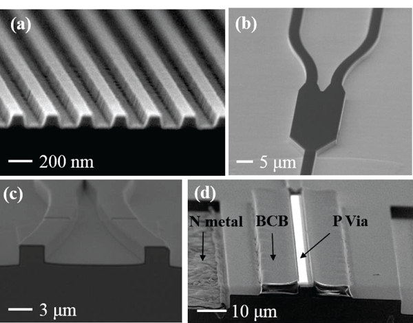
SEM images at various stages of the fabrication process: (a) The sampled gratings of the front mirror of the laser; (b) Top view of a 1×2 MMI structure; (c) Cross section of a MMI with silicon nitride passivation; (d) Cross section of the high-speed SOA.
For backend processing, the fabricated samples were thinned to less than 180-μm thickness and then PICs were cleaved. Fabricated transmitters have a footprint of 5.5 mm x 0.36 mm. PICs were solder mounted to ceramic carriers and wire-bonded for characterization. Device submounts were fixed to a temperature-controlled stage.
III. DEVICE CHARACTERIZATION
A. SGDBR laser
The widely tunable SGDBR laser, used as the integrated light source, consists of a rear absorber, back mirror, phase section, active gain section, and front mirror (see Fig. 1). The SGDBR laser has a 5-period front sampled grating mirror with 4-μm wide bursts and 68.5-μm period, a 12-period back sampled grating mirror with 6-μm wide bursts and 61.5-μm period [23, 24]. By controlling the injected current in the front and back mirrors, the emission wavelength can be tuned from 1521 nm to 1565 nm, demonstrating a 44-nm tuning range, thus covering more than the entire C-band. The tuning characteristics of the SGDBR laser are illustrated in Fig. 4, which presents the overlaid lasing spectra at various tuning conditions.
Fig. 4.

Overlaid lasing spectra of the SGDBR laser.
The light-current-voltage (LIV) characteristics were measured by using the reversed-biased high-speed integrated SOA as a photodetector. As shown in Fig. 5, the laser exhibits a threshold current of 45 mA and an output optical power of 15 mW at a gain section current of 100 mA; the peak power is well beyond 15 mW. The laser side mode suppression ratio (SMSR) across the tuning range is shown in Fig. 6, with a maximum SMSR of 55 dB at a wavelength near 1550 nm (see Fig. 7).
Fig. 5.
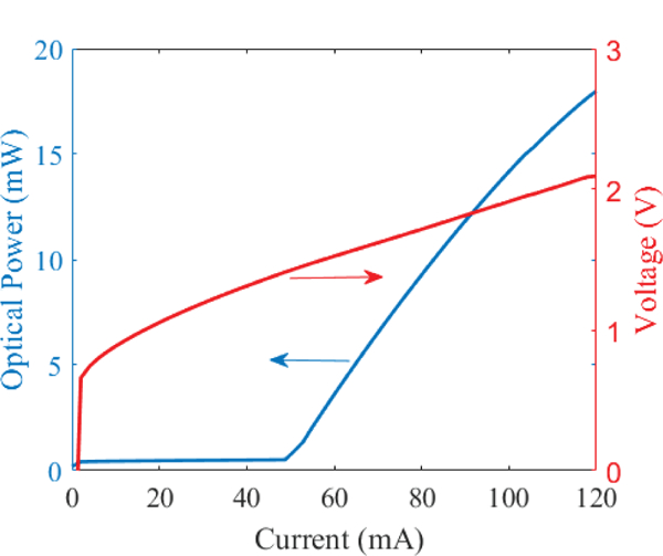
SGDBR laser LIV curve (with CW current source) measured by using the SOA as a photodiode.
Fig. 6.

Measured SMSR across the tuning range.
Fig. 7.
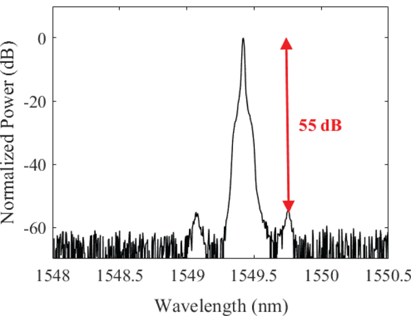
Lasing spectrum near 1550 nm with a 55-dB SMSR measured by an optical spectrum analyzer with a resolution bandwidth of 0.02 nm.
For laser linewidth characterization, the self-delayed heterodyne method was utilized and the measurement results are shown in Fig. 8 demonstrating a 3-dB linewidth of 6.4 MHz.
Fig. 8.

Measured heterodyne laser linewidth spectrum demonstrating a 3-dB linewidth of 6.4 MHz.
B. Mach-Zehnder modulator
During the p-cladding regrowth, the zinc doping diffuses into the InGaAsP waveguide layer, significantly increasing the device capacitance. To address this issue, some of the waveguide layer adjacent to the fabricated ridge was removed with a low-power reactive ion etch step following ridge formation [25]. Then a BCB layer was patterned where metal pads would be later deposited in order to further reduce parasitic pad capacitance.
Figure 9 and 10 report plots of the DC modulation characteristics (transfer functions) for the MZM under forward bias and reverse bias, respectively. Under forward bias, the MZM demonstrates an extinction ratio (ER) of 25 dB and half-wave voltage (Vπ) lower than 0.25 V at 1554 nm with approximately a 0.7-V forward voltage bias. Under reverse bias, the ER is 15 dB with a Vπ of −5.8 V. As expected, the MZM is significantly more efficient under forward bias. This is attractive especially for applications where an MZM is used for energy-efficient PPM for lower symbol rates. In this case, the MZM and high-speed SOA (SOA 1) would be simultaneously modulated by using two phase-aligned waveform generators.
Fig. 9.

MZM response under forward bias at various laser wavelengths.
Fig. 10.

MZM response under reverse bias at various laser wavelengths.
C. Semiconductor optical amplifier
The PIC transmitter comprises of two SOAs: a high-speed SOA for amplification/modulation and a two-section booster SOA with curved/angled and flared ridge waveguides. SOA 1 is 3 μm wide and 400 μm long. It is placed after the laser and before the MZM, to compensate for modulator insertion loss, and could also be used for modulation. The gain characteristics of the high-speed SOA at different input power levels are shown in Fig. 11.
Fig. 11.

Gain as a function of current density for the high-speed SOA (3 μm x 400 μm) with different input power levels at a wavelength of 1560 nm.
For SOA 2, it is constructed with two separate sections that can be pumped with different injection current levels, a scheme that may be utilized for optimizing power efficiency. The lengths of the two sections are 350 and 500 μm, respectively. The second section linearly flares from 3 μm to 5 μm, which reduces the optical power intensity thus enables an increased saturation power. This SOA at the transmitter output could potentially enable the PIC transmitter to be used in near-earth free space optical links without requiring an EDFA power amplifier.
IV. FREE SPACE OPTICAL LINK
To evaluate the transmitter performance, first a static characterization was performed. The transmitter optical output was coupled to an integrating sphere to measure the off-chip power. Figure 12 shows the off-chip power versus the current in the flared-waveguide section of the booster SOA. The current of the laser gain section, the SOA 1, and the first section of the SOA 2 are 150 mA, 110 mA and 90 mA, respectively. The maximum output power with the above DC biasing is 14.5 dBm (28 mW). The propagating loss of the curved and flared waveguides at the output is estimated to be 3 dB. The devices characterized were not anti-reflection (AR) coated, which would increase the coupled output power. Also, in future measurements with AR coated devices and improved heat sinking, it is expected that higher current levels can be achieved that will lead to higher measured output optical power.
Fig. 12.

Off-chip optical power of the PIC transmitter versus the current in the flared-waveguide section of the booster SOA.
To measure the high-speed performance of the transmitter, one arm of the MZM was wire bonded to a 50-Ω RF feeding transmission line and on the other side to a 50-Ω load mounted to the ceramic carrier. Figure 13 shows the eye diagrams for 1 Gbps and 3 Gbps non-return-to-zero (NRZ) OOK modulation at a reverse bias of −3.9 V. The extinction ratios (ER) are 13.4 dB and 16.8 dB, respectively.
Fig. 13.
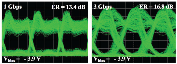
Eye diagrams for 1 Gbps and 3 Gbps NRZ OOK modulation.
Utilizing the fabricated InP PIC transmitter, a free space optical link was constructed as shown in Fig. 14. A NRZ 210 −1 pseudo random binary sequence (PRBS) was generated and applied to the MZM through a bias-Tee. The optical signal emitting from the transmitter was collected by a lensed single mode fiber (SMF) and coupled to an optical collimator (with a beam divergence angle of 0.016°), and then transmitted in air and collected by an identical collimator. The distance between the two collimators was 1.35 m. At the receiver side, an erbium doped fiber amplifier (EDFA) partially recovered the link loss and the signal was then detected by a PIN photodiode. An in-fiber variable optical attenuator (VOA) was used to simulate the attenuation of the free space optical link.
Fig. 14.
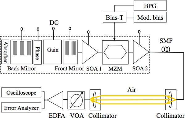
Schematic of free space optical link setup.
Bit error rate (BER) measurement results at 1 Gbps and 3 Gbps are shown in Fig. 15 as a function of the link attenuation. The free space link operates free of errors (BER < 1 × 10⁻⁹) up to approximately 24 dB attenuation (180 m distance) at the data rate of 3 Gbps. With forward error correction (BER < 2× 10⁻³), the equivalent link length can be up to 300 m (28 dB attenuation). At a lower date rate of 1 Gbps, the performance can be further improved. In this case, the corresponding link lengths at error free and forward error correction limit are 300 m and 400 m, respectively. A reference transmitter, consisting of a 10 GHz commercial MZM and an external cavity source, was also tested in the link under the same setting for comparison. The overall link length could be drastically increased with a booster high-power EDFA, which is commonly used in free space optical links.
Fig. 15.
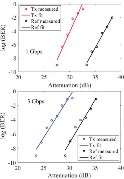
BER for 1 Gbps and 3 Gbps NRZ OOK transmission.
In future work, other energy-efficient modulation formats, such as PPM at lower symbol rates, will be demonstrated for free space optical links. On the other hand, higher data rate up to 40 Gbps can be achieved with more compact modulator designs. Instead of using offset quantum wells, a quantum well intermixing technique would eliminate the tradeoff between modulation efficiency and insertion loss. Furthermore, efforts will be made to improve the output optical power. Structures with ultra-low optical confinement factor in the active gain region would enable lower local optical intensity inside the SOAs, thus allowing for higher output saturation power.
V. CONCLUSION
An InP-based PIC transmitter was fabricated and characterized for free space optical communications. The SGDBR laser demonstrates a 44-nm tuning range and >45 dB SMSR across this range. With the high-power output SOA, the measured off-chip power was 14.5 dBm. The InP PIC transmitter was inserted in a free space optical link. Error-free operation was achieved at a data rate up to 3 Gbps with an equivalent link length of 180 m (up to 300 m with forward error correction).
Acknowledgments
Manuscript received Feb 1, 2018. This work was supported by a NASA Early Stage Innovations Award.
Biography
Hongwei Zhao received her B.S. degree from the Huazhong University of Science and Technology, Wuhan, China, in 2008, and the M.S. degree from the Institute of Semiconductors, Chinese Academy of Sciences, Beijing, China, in 2011. She is currently pursuing her PhD degree in Integrated Photonics Lab at the Electrical and Computer Engineering Department, University of California Santa Barbara, CA 93106. She is interested in silicon photonics with emerging materials (such as graphene, indium tin oxide), and compound semiconductor photonic integrated circuits. Her current research is focused on InP-based photonic integrated circuits for free space communications.
Sergio Pinna received the Ph.D. degree in Innovative Technologies from the Scuola Superiore Sant’Anna, Pisa, Italy, in 2014, and the B.Sc. and M.Sc. degrees in telecommunications engineering from University of Pisa, Pisa, Italy in 2008 and 2010 respectively. From November 2010 to December 2015 he was a fellow at CNIT at the National Photonic Networks Laboratory in Pisa. In 2014 he was visiting researcher at the Integrated Photonics Laboratory at Boston University, Boston, USA. From January 2016 he was a research fellow at TeCIP Institute, Scuola Superiore Sant’Anna, Pisa, Italy within the Digital and Microwave photonics group. In 2017 he joined the Integrated Photonics Laboratory at the University of California Santa Barbara as a Postdoctoral Research Associate.
Bowen Song received his Bachelor of Engineering Degree from the School of Electronic Engineering and Optoelectronic Technology at Nanjing University of Science and Technology (NJUST) of China in Nanjing in 2012. He is from Shanxi, China. He is currently a Ph.D. student in the Electrical and Computer Engineering Department at UCSB. In early 2013, he joined the Wide Bandgap Semiconductor Laboratory at Boston University working on developing nano-patterned sapphire substrate for AlGaN-based deep UV LEDs and received his Master of Science Degree in September 2014. His current research focuses on electronic-photonic integration, Integrated Photonics and integrated Lidar.
Ludovico Megalini received the Ph.D. degree in Materials from UCSB for his work on MOCVD growth, processing, and characterization of III-Nitride blue laser diodes. Previously he received a M.Sc. degree in ECE from UCSB for which he had been awarded a Fulbright Scholarship. He also holds a M.Sc. in Nanotechnology for ICT jointly awarded by PoliTO (IT), INPG (FR), and EPFL (CH), and had carried out the M.Sc. thesis project at MIT (USA). His past work experiences include positions as a business analyst at Accenture and as Senior Process Engineer at Crossbar-inc. His research interests are mainly focused on optoelectronics and nanotechnology, including the design, heteroeptiaxy growth, and fabrication of monolithically integrated lasers on silicon photonics.
Simone Tommaso Šuran Brunelli received his bachelor degree in Industrial Engineering with a thesis on semiconductor quantum dots, and a master degree in Materials Engineering with a thesis focused on atomic layer deposition, both at the Università degli Studi di Trieste. After a fellowship at Elettra Sincrotrone working on carbon nanotube synthesis and photoelectron spectroscopy, he joined the Integrated Photonics Lab at UCSB as a Ph.D. student. His current interests and duties revolve around metal organic chemical vapor deposition of III-V semiconductors for nanoelectronic and photonic applications including low-power tunneling transistors.
Larry A. Coldren (S’67-M’72-SM’77-F’82-LF’12) received the Ph.D degree in electrical engineering from Stanford University, Stanford, CA, USA, in 1972. After 13 years in the research area with Bell Laboratories, he joined the University of California at Santa Barbara (UCSB) in 1984. He is currently the Fred Kavli Professor of optoelectronics and sensors and holds appointments with the Department of Materials and the Department of Electrical and Computer Engineering. From 2009 to 2011, he was acting Dean of the College of Engineering. In 1990, he cofounded Optical Concepts, later acquired as Gore Photonics, to develop novel VCSEL technology, and, in 1998, he cofounded Agility Communications, later acquired by JDSU (now Lumentum), to develop widely tunable integrated transmitters. At UCSB, he worked on multiple-section widely tunable lasers and efficient vertical-cavity surface-emitting lasers (VCSELs). More recently, his group has developed high-performance InP-based photonic integrated circuits and high-speed, high-efficiency VCSELs. He has authored or coauthored more than a thousand journal and conference papers, eight book chapters, a widely used textbook, and 63 issued patents. He is a Fellow of OSA, IEEE, and the National Academy of Inventors, as well as a member of the National Academy of Engineering. He received the 2004 John Tyndall Award, the 2009 Aron Kressel Award, the 2014 David Sarnoff Award, the 2015 IPRM Award, and the 2017 Nick Holonyak, Jr. Award.
Jonathan Klamkin received the B.S. degree from Cornell University, Ithaca, NY, USA and the M.S. and Ph.D. degrees from the University of California Santa Barbara, Santa Barbara, CA, USA. From 2008 to 2011, he was a member of the Technical Staff in the Electro-Optical Materials and Devices Group, MIT Lincoln Laboratory, Lexington, MA, USA. From 2011 to 2013, he was an Assistant Professor at the Institute of Communication, Information and Perception Technologies at the Scuola Superiore Sant’Anna, Pisa, Italy. From 2013 to 2015, he was an Assistant Professor of Electrical and Computer Engineering (ECE) and Materials at Boston University, Boston, MA, USA. In 2015, he joined the ECE Department at the University of California Santa Barbara, where he is currently an Associate Professor. He is an Associate Editor for Photonics Technology Letters and the Vice Chair for the Microwave Theory and Techniques Society Subcommittee on Microwave Photonics. He was Program Chair for the Integrated Photonics Research, Silicon and Nanophotonics Conference, in 2017, and is serving as General Chair for the same conference, in 2018. He or his group members received best paper awards at the 2006 Conference on Optoelectronic and Microelectronic Materials and Devices and the 2007 Microwave Photonics Conference, and the 2017 Asia Communications and Photonics Conference. He also received the NASA Early Career Faculty Award and DARPA Young Faculty Award. Prof. Klamkin is a senior member of the IEEE and OSA.
Contributor Information
Hongwei Zhao, Department of Electrical and Computer Engineering, University of California Santa Barbara, Santa Barbara, CA 93106, USA (hwzhao@ece.ucsb.edu)..
Sergio Pinna, Department of Electrical and Computer Engineering, University of California Santa Barbara, Santa Barbara, CA 93106, USA (pinna@ece.ucsb.edu)..
Bowen Song, Department of Electrical and Computer Engineering, University of California Santa Barbara, Santa Barbara, CA 93106, USA (bowen@ece.ucsb.edu;.
Ludovico Megalini, Department of Electrical and Computer Engineering, University of California, Santa Barbara, CA 93106, USA. He is with Infineon Technologies, Italy (megalini@engineering.ucsb.edu)..
Simone Tommaso Šuran Brunelli, Department of Electrical and Computer Engineering, University of California Santa Barbara, Santa Barbara, CA 93106, USA (ssuranbrunelli@umail.ucsb.edu)..
Larry A. Coldren, Department of Electrical and Computer Engineering, University of California Santa Barbara, Santa Barbara, CA 93106, USA (coldren@ucsb.edu)..
Jonathan Klamkin, Department of Electrical and Computer Engineering, University of California Santa Barbara, Santa Barbara, CA 93106, USA (klamkin@ucsb.edu)..
REFERENCES
- [1].Hemmati H, Biswas A, and Djordjevic IB, “Deep-space optical communications: future perspectives and applications,” Proceedings of the IEEE, vol. 99, no. 11, pp. 2020–2039, Nov. 2011. [Google Scholar]
- [2].Caplan DO, “Laser communication transmitter and receiver design,” J. Opt. Fiber Commun. vol. 4, pp. 225—362, 2007. [Google Scholar]
- [3].Kingsbury RW, Caplan DO, and Cahoy KL, “Compact optical transmitters for Cubesat free-space optical communications,” Proc. of SPIE, Free-Space Laser Communication and Atmospheric Propagation, 2015, pp. 9354. [Google Scholar]
- [4].Cesarone RJ, Abrahams DS, Shambayati S, and Rush J, “Deep space communications visions trends and prospects”, in Proc. Int. Conf. Space Opt. Syst. Appl., 2011, pp. 412–425. [Google Scholar]
- [5].Rosborough V, Gambini F, Snyder J, Johansson L, and Klamkin J, “Integrated transmitter for deep space optical communications,” in Proc. Conf. IEEE Avionics and Vehicle Fiber-Optics and Photonics (AVFOP), 2016, pp. 207–208. [Google Scholar]
- [6].Su T, Ryan P Scott Stevan S. Djordjevic NK Fontaine David J. Geisler X Cai SJ Yoo B, “Demonstration of free space coherent optical communication using integrated silicon photonic orbital angular momentum devices,” Opt. Express, vol. 20, no.9, pp. 9396–9402, 2012. [DOI] [PubMed] [Google Scholar]
- [7].Fridlander J, Pinna S, Rosborough V, Estrella S, Johansson L, and Klamkin J, “RZ-DPSK photonic integrated transmitter for space optical communications,” in Proc. SPIE Photonics West, 2018, paper 10524–34. [Google Scholar]
- [8].Rosborough V, Gambini F, Snyder J, Johansson L, and Klamkin J “Integrated indium phosphide pulse position modulation transmitter for free space communications,” in Proc. Advanced Photonics 2016. (IPR, NOMA, Sensors, Networks, SPPCom, SOF; ), paper ITu2A.3. [Google Scholar]
- [9].Zhao H, Pinna S, Song B, Megalni L, Šuran Brunelli ST, Coldren L, and Klamkin J “High-power integrated indium phosphide transmitter for free space communications,” in Proc. Conf. on Lasers and Electro-Optics 2018, paper JW2A.52. [DOI] [PMC free article] [PubMed] [Google Scholar]
- [10].Zhao H, Pinna S, Song B, Megalni L, Šuran Brunelli ST, Coldren L, and Klamkin J “Integrated indium phosphide transmitter for free space optical link,” in Proc. Advanced Photonics 2018. (IPR, NOMA, Sensors, Networks, SPPCom, SOF; ), paper ITu4B.6. [DOI] [PMC free article] [PubMed] [Google Scholar]
- [11].Coldren LA, Nicholes SC, Johansson L, Ristic S, Guzzon RS, Norberg EJ, and Krishnamachari U, “High performance InP-based photonic ICs—a tutorial,” J. of Lightw. Technol, vol. 29, no. 4, pp. 554–570, 2011. [Google Scholar]
- [12].Smit M, et al. , “An introduction to InP-based generic integration technology,” Semicond. Sci. Technol, vol 29, no. 8, pp.083001–0830041, 2014. [Google Scholar]
- [13].Nagarajan R, et al. , “Large-scale photonic integrated circuits,” IEEE J. Sel. Top. Quant. Electron, vol.11, no. 1, pp. 50–65, 2005. [Google Scholar]
- [14].Corzine SW, et al. , “Large-scale InP transmitter PICs for PM-DQPSK fiber transmission systems,” IEEE Photonics Technology Letters, vol. 22, no. 14, pp. 1015–1017, July15, 2010. [Google Scholar]
- [15].Nicholes SC, Mašanović ML, Jevremović B, Lively E, Coldren LA, and Blumenthal DJ, “The world’s first InP 8×8 monolithic tunable optical router (MOTOR) operating at 40 Gbps line rate per port,” in Proc. Conf. Optical Fiber Communication Conference and National Fiber Optic Engineers, 2009, paper PDPB1. [Google Scholar]
- [16].Juodawlkis PW, Plant JP, Loh W, Missaggia LJ, O’Donnell FJ, Oakley DC, Napoleone A, Klamkin J, Gopinath JT, Ripin DJ, Gee S, Delfyett PJ, and Donnelly JP, “High-power, low-noise 1.5-μm slab-coupled optical waveguide (SCOW) emitters: physics, devices, and applications,” IEEE J. Quant. Elec, vol. 17, pp. 1698–1714, 2011. [Google Scholar]
- [17].Raring JW, Johansson LA, Skogen EJ, Sysak MN, Poulsen HN, DenBarras SP, and Coldren LA, “40 Gbit/s photonic receivers integrating UTC photodiodes with high- and low-confinement SOAs using quantum well intermixing and MOCVD regrowth,” Electron. Lett, vol. 42, no. 16, pp. 942–943, 2006. [Google Scholar]
- [18].Dummer MM, Klamkin J, Tauke-Pedretti A, and Coldren LA, “40 Gb/s field-modulated wavelength converters for all-optical packet switching”, IEEE J. Sel. Topics Quantum Electron., vol. 15, no. 3, pp. 494–503, 2009. [Google Scholar]
- [19].Summers J, et al. , “40 Channels x 57 Gb/s monolithically integrated InP-based coherent photonic transmitter,” in Proc. European Conference on Optical Communication (ECOC), 2014, paper P.2.5. [Google Scholar]
- [20].Lal V, et al. , “Extended C-band tunable multi-channel InP-based coherent transmitter PICs,” J. of Lightw. Technol, vol. 35, no. 7, pp. 1320–1327, 2017. [Google Scholar]
- [21].Jayaraman LCV, Chuang ZM, and Coldren LA, “Theory, design, and performance of extended tuning range semiconductor lasers with sampled gratings,” IEEE J. Quantum Electron., vol. 29, no. 6, pp. 1824–1834, Jun. 1993. [Google Scholar]
- [22].Coldren LA, “Monolithic tunable diode lasers,” IEEE J. Sel. Topics Quantum Electron., vol. 6, no. 6, pp. 988–999, 2000. [Google Scholar]
- [23].Mason B, Barton J, Fish GA, Coldren LA, and DenBaars SP, “Design of sampled grating DBR lasers with integrated semiconductor optical amplifiers,” IEEE Photon. Technol. Lett, vol. 12, no.7, pp. 762–764, Jul. 2000. [Google Scholar]
- [24].Barton JS, Skogen EJ, Masanovic ML, Denbaars SP, and Coldren LA, “A widely tunable high-speed transmitter using an integrated SGDBR laser-semiconductor optical amplifier and Mach-Zehnder modulator,” IEEE J. Sel. Topics Quantum Electron., vol. 9, no. 5, pp. 1113–1117, 2003. [Google Scholar]
- [25].Barton JS, “The integration of Mach-Zehnder modulators with sampled grating DBR lasers”, PhD dissertation, Dept. Electrical and Computer Eng., University of California, Santa Barbra, USA, 2004. [Google Scholar]


