Abstract
Here, large-scale and uniform hexagonal zinc oxide (ZnO) nanosheet films were deposited onto indium tin oxide (ITO)-coated transparent conducting glass substrates via a facile galvanic displacement deposition process. Compared with other commonly used solution methods, this process avoids high temperature and electric power as well as supporting agents to make it simple and cost-effective. The as-fabricated ZnO nanosheet films have uniform hexagonal wurtzite structure. The photoelectrochemical (PEC) cell based on ZnO nanosheet film/ITO photoelectrode was also fabricated and its performance was improved by optimizing the solution concentration. A higher photocurrent density of ~500 μA cm−2 under AM 1.5 G simulated illumination of 100 mW cm−2 with zero bias potential (vs. Ag/AgCl electrode) was obtained, which may ascribe to the increased surface-to-volume ratio of disordered ZnO nanosheet arrays. Our developed method may be used to deposit other oxide semiconductors, and the ZnO nanosheet film/ITO PEC cell can be used to design low-cost optoelectronic and photoelectrochemical devices.
Keywords: Zinc oxide, Nanosheet film, Self-assemble, Galvanic displacement method, Photoelectrochemical property
Introduction
Over the past decades, there has been an increasing scientific interest in oxide semiconductors (such as TiO2, ZnO, Fe2O3, CuO, NiO, and so on) [1–3], because of their numerous potential technological applications, including photovoltaic device [4], lithium ion battery [5], photocatalysis, and optoelectronic device [6, 7]. Among the oxide semiconductors, ZnO as a prototypical n-type conducting oxide has attracted considerable attentions for wide usages in piezoelectric device, ultraviolet optoelectronics detectors [8, 9], low-cost dye-sensitized solar cells [10], gas sensors [11, 12], photocatalysis, and photoelectrochemical (PEC) devices [13, 14]. Most of these applications are based on the advantages of its abundance, low cost, non-toxicity, chemical stability and the possibility of growing ordered nanostructures, and strong exciton binding energy [15]. Especially, nanostructured ZnO exhibits enhanced performance and provided an ideal system to study the influence of surface effects and interface science on photoelectrochemical properties due to their large surface-to-volume ratios [16–18].
To date, ZnO and other nanostructured materials have been assembled and studied by various methods and means [19–22], including magnetron sputtering [23], chemical vapor deposition [24], hydrothermal process [25], electrochemical deposition [26–28], electroless deposition [29, 30], and other combination of methods [31]. Among all these techniques, electroless deposition presents several advantages such as low cost, large-scale deposition, and low-temperature processing. Here, we explored a facile solution-based galvanic displacement deposition technique to self-assembly synthesis uniform hexagonal ZnO nanosheet film on ITO glass substrate under ambient conditions. ZnO nanosheet film/ITO PEC cell and its photoelectrochemical property were also investigated.
Experimental Details
Synthesis of the ZnO Nanosheet Films
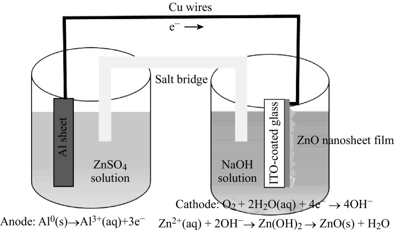
Compared with other common electrodeposition methods, an electroless deposition process was employed to fabricate ZnO nanosheets. A typical galvanic cell system with two half-cells (A and B) was used to generate a current by coupling oxidation and reduction reactions in a spontaneous process, in which the A cell solution is 5–15 mM ZnSO4 and the B cell solution is 0.25 M NaOH. The two half-cells were connected by a porous salt bridge that supplied ions to maintain charge neutrality during current flow. The galvanic cell deposition system is composed of Al sheet (99.99 % purity) and ITO conducting glass (sheet resistance of 10 Ω cm−2), which acted as anode and cathode, respectively. The two electrodes were short-circuited externally through a metal copper wire. Before deposition, 4 cm × 2 cm Al sheet and ITO glass were, respectively, cleaned in acetone, ethanol, and deionized water for 5 min. Then, the Al sheet was immerged into A cell solution and the ITO glass was immerged into B cell solution without stirring and oxygen gas bubbling at room temperature. In order to obtain higher crystal quality, the as-prepared samples were annealed at 550 °C for 60 min with the increasing rate of 10 °C min−1 in an air atmosphere.
Characterization
The surface morphology of the as-deposited ZnO nanosheet films was obtained by field emission scanning electron microscopy (FE-SEM; FEI Sirion 200, Holland). A D8 ADVANCE DA VINCI X-ray diffractometer (XRD, Bruker, German) was employed to verify the crystal structure of the samples using Cu Kα radiation (λ = 0.15418 nm) with a scanning rate of 5° min−1. The photoluminescence (PL) spectrum of the as-resulting ZnO films was obtained using the Jobin–Yvon LabRam HR 800 UV system with a 325-nm laser at room temperature. The UV–Vis spectra of the ZnO samples were obtained through UV–Vis spectrophotometer (PerkinElmer Lambda 950, America).
PEC Cell Preparation and PEC Characterization
PEC cell was fabricated by placing a copper wire onto a bare portion of the ITO conducting substrate and securing with high-purity silver conducting glue. Then, the part active area of ZnO nanosheet films was sealed with epoxy resin leaving an exposed working electrode surface area of 1 cm × 1 cm. An electrochemical workstation (Princeton Applied Research, PARSTAT 4000, America) was used to study the photoelectrochemical property of the samples. The photoelectrochemical experiment was performed in a conventional three electrode, in which the resulting ZnO nanosheet film/ITO substrate acted as working electrode (illuminating area of 1 cm2), a platinum net (surface area of 1 cm2) as counter electrode, and an Ag/AgCl as reference electrode. The PEC experiments were carried out in a mixture solution of 0.35 M Na2S and 0.25 M Na2SO3 under AM 1.5 G (100 mW cm−2) simulated illumination, which was provided by a 300 W xenon lamp (Beijing Perfectlight Technology, PLS-SXE300C, China) equipped with an AM 1.5 filter. The illumination intensity was measured with a solar simulator spectroradiometer (EKO instrument, LS-100, Japan).
Results and Discussion
The schematic drawing of the experimental setup used for the fabrication ZnO nanosheet films is shown in Fig. 1. When the Al electrode, connected with the ITO glass externally, was dipped into the NaOH solution, Al3+ ions formed in the solution due to the dissolution of Al foil. Then, the released electrons moved through the externally short-circuited path to the ITO electrode. At the same time, the electron prompted the basic electrochemical reduction of oxygen (O2) in the aqueous solution, and then led to the formation of OH− ions on ITO substrate surface. Finally, the Zn2+ ions in the solution were attracted by the corresponding OH− ions on the ITO surface, and an intermediate Zn(OH)2 was formed and rapidly converted to ZnO. The growth mechanism of ZnO nanosheet film has similar electrochemical reaction with the electrodeposition [32]. The reactions may be as follows:
Fig. 1.
The schematic drawing of the experimental setup used for the fabrication of hexagonal ZnO nanosheet films
In the process of nanosheet film formation, ZnO nanocrystals were primarily generated and then they were self-assembled into ordered hexagon nanostructure. These staggered arrangement nanosheet formed ZnO film in the substrate surface finally. Actually, semiconductor self-assembly is a complex phenomenon that depends on the interplay of several physical factors and competing interactions of different nature. A thorough understanding of the self-assembly mechanism of nanocrystals to organize into ordered nanostructure is one of the keys of future nanoscience [33].
Figure 2 shows FE-SEM images of the top and side view of the hexagonal ZnO nanosheet films grown on the ITO substrate at 5 and 10 mM ZnSO4 aqueous solution for 2 h, and annealed at 550 °C for 1 h. One can see that the ZnO had quite perfect hexagon and large-scale irregular arrangement. The samples shown in Fig. 2a, b were, respectively, grown at 5 mM ZnSO4 solution and 10 mM ZnSO4. It can be seen that the concentration of ZnSO4 aqueous solution plays an important role in the size and thickness of hexagonal ZnO nanosheets, as well as the surface-to-volume ratios.
Fig. 2.
FE-SEM images of the as-prepared hexagonal ZnO nanosheet films grown on the ITO-coated glass substrate with different concentrations of ZnSO4. a 5 mM and b 10 mM, top view. c 10 mM, side view
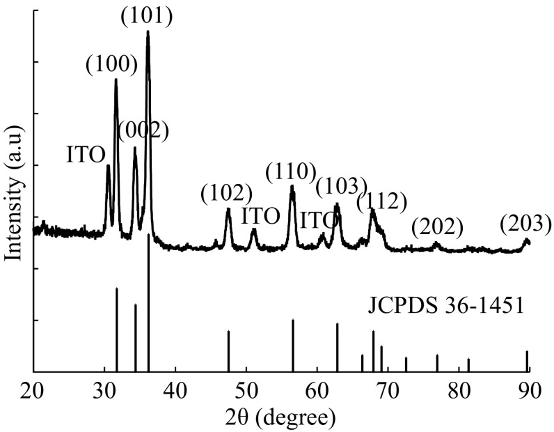
Figure 3 shows XRD pattern of the hexagonal ZnO nanosheet films on ITO by electroless depositing at 7.5 mM ZnSO4 for 2 h under room temperature and post-annealing at 550 °C for 1 h in open air conditions. All diffraction peaks correspond to the standard diffraction of a hexagonal wurtzite ZnO crystal (JCPDS 36-1451) [34]. The major diffraction peaks have sharp features, corresponding to the (100), (002), (101), (102), (110), (103), and (112) planes, which is due to the disorder arrangement of ZnO nanosheets on the ITO. At the same time, the peaks from the ITO conducting substrates were observed as well.
Fig. 3.
XRD pattern of the as-annealed hexagonal ZnO nanosheet film at 550 °C in open air conditions
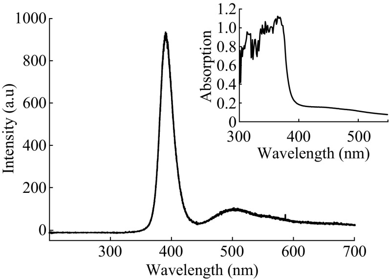
Figure 4 exhibits the representative room temperature PL spectrum of the ZnO nanosheet films grown in 7.5 mM ZnSO4 aqueous solution and annealed at 550 °C for 1 h. A laser with wavelength of 325 nm was used as the excitation source. The strong UV emission peak at about 390 nm could be usually attributed to the free exciton emission from the wide band-gap ZnO [35]. The lower broad peak around 500 nm is usually considered to be the recombination of a photogenerated hole with the single ionized charged state of the defect in ZnO and could be related to the surface oxygen vacancies of the ZnO because the ZnO nanosheet films have much high surface-to-volume ratios [36]. The PL spectrum result indicates that the as-prepared ZnO has few defects [37]. The inset image in Fig. 4 shows the UV–Vis absorption spectrum of this sample, indicating its band gap at nearly 3.25 eV. The band-gap values of ZnO film were calculated by Tauc plot [38, 39].
Fig. 4.
Room temperature photoluminescence spectrum of the as-prepared ZnO nanosheet film. Excitation wavelength: 325 nm. The inset picture is the UV–Vis absorption spectrum of the same sample
The photoelectrochemical property of ZnO nanosheet thin film/ITO electrode was measured with an electrochemical workstation. All PEC measurement was carried out in a mixture solution of 0.35 M Na2S and 0.25 M Na2SO3 under AM 1.5 G (100 mW cm−2). Figure 5 shows the photoelectrochemical property of ZnO nanosheet thin film/ITO electrode. Its photocurrent was investigated under a bias voltage of 0 V (vs. Ag/AgCl) with a light on–off interval of 20 s, as shown in Fig. 5a. All PEC cell exhibits significant photoresponse under a bias voltage of 0 V (vs. Ag/AgCl), but the sample fabricated at 7.5 mM solution has superior characteristics with a higher photocurrent of 500 μA cm−2. The photocurrent density of the photoelectrode varies with the different growth concentrations of ZnSO4 aqueous solution, which may be related to the resistance and surface-to-volume ratio of the samples that could affect the light absorption. Linear sweep voltammograms (LSV) curves were recorded for the 7.5 mM sample in the dark and at 100 mW cm−2 (AM 1.5) with a scan rate of 10 mV s−1 in the applied potentials from −1 to +1 V (vs. Ag/AgCl), as shown in Fig. 5b. The dark scan shows a very small current density in the range of 10 μA cm−2, whereas under light illumination a pronounced photocurrent density was observed, implying efficient charge separation and transfer in this nanostructured ZnO. Figure 5c shows the chronoamperometric plots of the ZnO/ITO electrode for about 1 h, which indicated that the photoelectrochemical property was fairly stable under illumination. The photocurrent did not obviously decrease which is very important for the development of practical PEC cells.
Fig. 5.
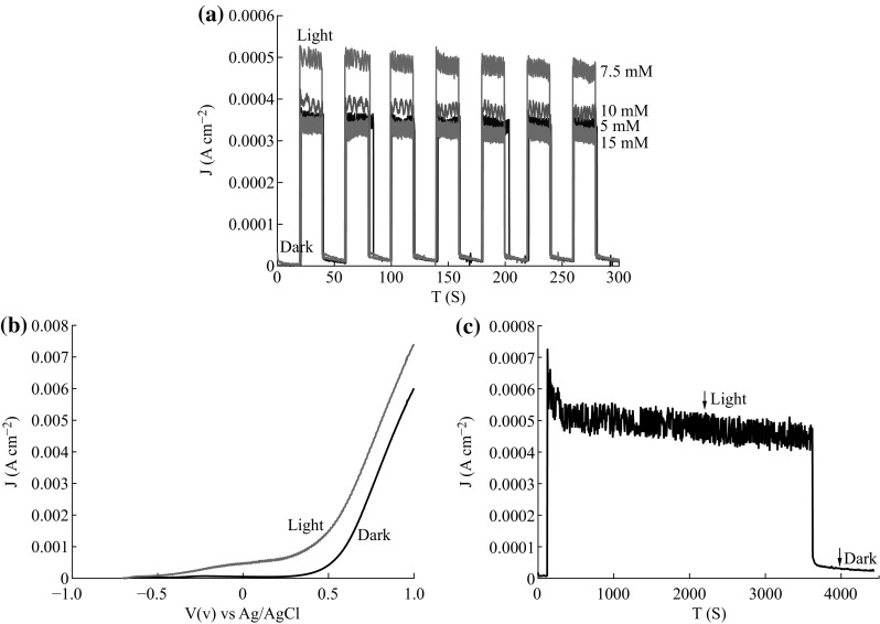
The photoelectrochemical properties of the ZnO nanosheet thin film/ITO electrode. a Chronoamperometry measurements at zero bias potential (vs. Ag/AgCl electrode) under chopped light illumination with a light on–off interval of 20 s. b LSV curves recorded for the 7.5 mM sample with a scan rate of 10 mV s−1 in the applied potentials from −1 to +1 V (vs. Ag/AgCl). c The J − T stability of electrode. All PEC experiments were carried out in a mixture solution of 0.35 M Na2S and 0.25 M Na2SO3 under AM 1.5 G (100 mW cm−2)
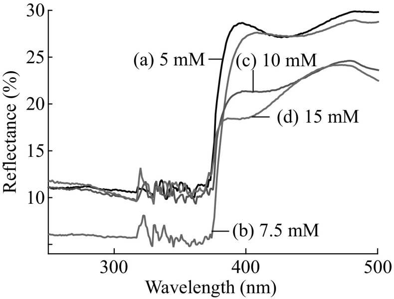
In order to further understand the photoelectrochemical property of ZnO nanosheet films, the UV–Vis reflectance spectra were also measured by PerkinElmer Lambda 950 UV–Vis spectrophotometer. Figure 6 shows the UV–Vis reflection spectra of the ZnO nanosheet films grown at different concentrations of ZnSO4. It can be seen that the 7.5 mM sample had a maximum ultraviolet absorption compared to other samples. The reflectance spectra result was consistent with the photoelectrochemical result. These results clearly demonstrated that the PEC performance strongly depended on the morphology of ZnO and could be optimized through controlling the material growth condition.
Fig. 6.
Reflectance spectra of ZnO sheet films on ITO glass grown at different concentrations of ZnSO4. a 5 mM, b 7.5 mM, c 10 mM, d 15 mM
Conclusion
In this paper, we had presented a simple and highly efficient solution-based method to prepare large-scale hexagonal ZnO nanosheet films using a galvanic displacement reaction. The advantages of this solution-processing technique are its simplicity as well as it does not need electric power and supporting agents. The hexagonal ZnO nanosheet films prepared by this method exhibited excellent PEC properties. These results indicated that the ZnO nanosheet film could be applied in low-cost, high-performance photoelectrochemical devices or other application fields.
Acknowledgments
We were grateful to Linna. Pang for assistance with PL spectrum. This work was supported by the National Major Basic Research Project of 2012CB934302, the National 863 Program 2011AA050518, and the Natural Science Foundation of China (Grant No. 11174197, 11574203 and 61234005).
References
- 1.Kochuveedu ST, Jang YH, Kim DH. A study on the mechanism for the interaction of light with noble metal-metal oxide semiconductor nanostructures for various photophysical applications. Chem. Soc. Rev. 2013;42(21):8467–8493. doi: 10.1039/c3cs60043b. [DOI] [PubMed] [Google Scholar]
- 2.Zhou H, Wong SS. A facile and mild synthesis of 1-D ZnO, CuO, and α-Fe2O3 nanostructures and nanostructured arrays. ACS Nano. 2008;2(5):944–958. doi: 10.1021/nn700428x. [DOI] [PubMed] [Google Scholar]
- 3.Comini E, Baratto C, Faglia G, Ferroni M, Vomiero A, Sberveglieri G. Quasi-one dimensional metal oxide semiconductors: preparation, characterization and application as chemical sensors. Prog. Mater. Sci. 2009;54(1):1–67. doi: 10.1016/j.pmatsci.2008.06.003. [DOI] [Google Scholar]
- 4.Lira-Cantu M, Krebs FC. Hybrid solar cells based on MEH-PPV and thin film semiconductor oxides (TiO2, Nb2O5, ZnO, CeO2 and CeO2–TiO2): performance improvement during long-time irradiation. Sol. Energy Mater. Sol. Cells. 2006;90(14):2076–2086. doi: 10.1016/j.solmat.2006.02.007. [DOI] [Google Scholar]
- 5.Park KT, Xia F, Kim SW, Kim SB, Song T, Paik U, Park WI. Facile synthesis of ultrathin ZnO nanotubes with well-organized hexagonal nanowalls and sealed layouts: applications for lithium ion battery anodes. J. Phys. Chem. C. 2013;117(2):1037–1043. doi: 10.1021/jp310428r. [DOI] [Google Scholar]
- 6.Niu M, Huang F, Cui L, Huang P, Yu Y, Wang Y. Hydrothermal synthesis, structural characteristics, and enhanced photocatalysis of SnO2/α-Fe2O3 semiconductor nanoheterostructures. ACS Nano. 2010;4(2):681–688. doi: 10.1021/nn901119a. [DOI] [PubMed] [Google Scholar]
- 7.Guo T, Luo Y, Zhang Y, Lin Y-H, Nan C-W. Controllable growth of ZnO nanorod arrays on NiO nanowires and their high UV photoresponse current. Cryst. Growth Des. 2014;14(5):2329–2334. doi: 10.1021/cg500031t. [DOI] [Google Scholar]
- 8.Wang ZL, Kong XY, Ding Y, Gao P, Hughes WL, Yang R, Zhang Y. Semiconducting and piezoelectric oxide nanostructures induced by polar surfaces. Adv. Funct. Mater. 2004;14(10):943–956. doi: 10.1002/adfm.200400180. [DOI] [Google Scholar]
- 9.Fang X, Bando Y, Gautam UK, Zhai T, Zeng H, Xu X, Liao M, Golberg D. ZnO and ZnS nanostructures: ultraviolet-light emitters, lasers, and sensors. Crit. Rev. Solid State. 2009;34(3–4):190–223. doi: 10.1080/10408430903245393. [DOI] [Google Scholar]
- 10.Xi YY, Hsu YF, Djurišić AB, Chan WK. Electrochemical synthesis of ZnO nanoporous films at low temperature and their application in dye-sensitized solar cells. J. Electrochem. Soc. 2008;155(9):D595. doi: 10.1149/1.2952519. [DOI] [Google Scholar]
- 11.Zhang Y, Xu J, Xiang Q, Li H, Pan Q, Xu P. Brush-like hierarchical ZnO nanostructures: synthesis, photoluminescence and gas sensor properties. J. Phys. Chem. C. 2009;113(9):3430–3435. doi: 10.1021/jp8092258. [DOI] [Google Scholar]
- 12.Kumar R, Al-Dossary O, Kumar G, Umar A. Zinc oxide nanostructures for NO2 gas–sensor applications: a review. Nano-Micro Lett. 2014;7(2):97–120. doi: 10.1007/s40820-014-0023-3. [DOI] [PMC free article] [PubMed] [Google Scholar]
- 13.Ho-Kimura S, Moniz SJA, Tang J, Parkin IP. A method for synthesis of renewable Cu2O junction composite electrodes and their photoelectrochemical properties. ACS Sustain. Chem. Eng. 2015;3(4):710–717. doi: 10.1021/acssuschemeng.5b00014. [DOI] [Google Scholar]
- 14.Wu M, Chen WJ, Shen YH, Huang FZ, Li CH, Li SK. In situ growth of matchlike ZnO/Au plasmonic heterostructure for enhanced photoelectrochemical water splitting. ACS Appl. Mater. Interf. 2014;6(17):15052–15060. doi: 10.1021/am503044f. [DOI] [PubMed] [Google Scholar]
- 15.Winget P, Schirra LK, Cornil D, Li H, Coropceanu V, et al. Defect-driven interfacial electronic structures at an organic/metal-oxide semiconductor heterojunction. Adv. Mater. 2014;26(27):4711–4716. doi: 10.1002/adma.201305351. [DOI] [PubMed] [Google Scholar]
- 16.Biswas M, Jung YS, Kim HK, Kumar K, Hughes GJ, Newcomb S, Henry MO, McGlynn E. Microscopic origins of the surface exciton photoluminescence peak in ZnO nanostructures. Phys. Rev. B. 2011;83(23):235320. doi: 10.1103/PhysRevB.83.235320. [DOI] [Google Scholar]
- 17.Chen Z, Tang Y, Zhang L, Luo L. Electrodeposited nanoporous ZnO films exhibiting enhanced performance in dye-sensitized solar cells. Electrochim. Acta. 2006;51(26):5870–5875. doi: 10.1016/j.electacta.2006.03.026. [DOI] [Google Scholar]
- 18.Zhang Q, Dandeneau CS, Zhou X, Cao G. ZnO nanostructures for dye-sensitized solar cells. Adv. Mater. 2009;21(41):4087–4108. doi: 10.1002/adma.200803827. [DOI] [Google Scholar]
- 19.Saha A, Jiang C, Martí AA. Carbon nanotube networks on different platforms. Carbon. 2014;79:1–18. doi: 10.1016/j.carbon.2014.07.060. [DOI] [Google Scholar]
- 20.Xu T, Davis VA. Liquid crystalline phase behavior of silica nanorods in dimethyl sulfoxide and water. Langmuir. 2014;30(16):4806–4813. doi: 10.1021/la405013h. [DOI] [PubMed] [Google Scholar]
- 21.Zhang H, Ding W, He K, Li M. Synthesis and characterization of crystalline silicon carbide nanoribbons. Nanoscale Res. Lett. 2010;5(8):1264–1271. doi: 10.1007/s11671-010-9635-9. [DOI] [PMC free article] [PubMed] [Google Scholar]
- 22.Zhang K, Kim SJ, Zhang Y, Heeg T, Schlom DG, Shen W, Pan X. Epitaxial growth of ZnO on (1 1 1) Si free of an amorphous interlayer. J. Phys. D-Appl. Phys. 2014;47(10):105302. doi: 10.1088/0022-3727/47/10/105302. [DOI] [Google Scholar]
- 23.Kumar R, Khare N, Kumar V, Bhalla GL. Effect of intrinsic stress on the optical properties of nanostructured ZnO thin films grown by rf magnetron sputtering. Appl. Surf. Sci. 2008;254(20):6509–6513. doi: 10.1016/j.apsusc.2008.04.012. [DOI] [Google Scholar]
- 24.Cheng A-J, Tzeng Y, Zhou Y, Park M, Wu T-H, Shannon C, Wang D, Lee W. Thermal chemical vapor deposition growth of zinc oxide nanostructures for dye-sensitized solar cell fabrication. Appl. Phys. Lett. 2008;92(9):092113. doi: 10.1063/1.2889502. [DOI] [Google Scholar]
- 25.Baruah S, Dutta J. Hydrothermal growth of ZnO nanostructures. Sci. Technol. Adv. Mater. 2009;10(1):013001. doi: 10.1088/1468-6996/10/1/013001. [DOI] [PMC free article] [PubMed] [Google Scholar]
- 26.O’Regan B, Sklover V, Grätzel M. Electrochemical deposition of smooth and homogeneously mesoporous ZnO films from propylene carbonate electrolytes. J. Electrochem. Soc. 2001;148(7):C498. doi: 10.1149/1.1377899. [DOI] [Google Scholar]
- 27.Park HK, Hong SP, Do YR. Vertical growth of ZnO nanorods prepared on an ITO-coated glass substrate by hydrothermal-electrochemical deposition. J. Electrochem. Soc. 2012;159(6):D355. doi: 10.1149/2.078206jes. [DOI] [Google Scholar]
- 28.Hambali NA, Hashim AM. Synthesis of zinc oxide nanostructures on graphene/glass substrate via electrochemical deposition: effects of potassium chloride and hexamethylenetetramine as supporting reagents. Nano-Micro Lett. 2015;7(4):317–324. doi: 10.1007/s40820-015-0045-5. [DOI] [PMC free article] [PubMed] [Google Scholar]
- 29.Wang L, Liu G, Xue D. Effects of introduced electrolytes on galvanic deposition of ZnO films. Electrochim. Acta. 2010;55(22):6796–6801. doi: 10.1016/j.electacta.2010.05.088. [DOI] [Google Scholar]
- 30.Nagaya S, Nishikiori H. Preparation of dye-adsorbing ZnO thin films by electroless deposition and their photoelectrochemical properties. ACS Appl. Mater. Interf. 2013;5(18):8841–8844. doi: 10.1021/am4026483. [DOI] [PubMed] [Google Scholar]
- 31.Emin S, Fanetti M, Abdi FF, Lisjak D, Valant M, van de Krol R, Dam B. Photoelectrochemical properties of cadmium chalcogenide-sensitized textured porous zinc oxide plate electrodes. ACS Appl. Mater. Interf. 2013;5(3):1113–1121. doi: 10.1021/am3027986. [DOI] [PubMed] [Google Scholar]
- 32.Goux A, Pauporté T, Chivot J, Lincot D. Temperature effects on ZnO electrodeposition. Electrochim. Acta. 2005;50(11):2239–2248. doi: 10.1016/j.electacta.2004.10.007. [DOI] [Google Scholar]
- 33.C. Melis, P. Raiteri, L. Colombo, A. Mattoni, Self-assembling of zinc phthalocyanines on ZnO () surface through multiple time scales. ACS Nano 5(12), 9639–9647 (2011). doi:10.1021/nn203105w [DOI] [PubMed]
- 34.Chen X, Jing X, Wang J, Liu J, Song D, Liu L. Self-assembly of ZnO nanoparticles into hollow microspheres via a facile solvothermal route and their application as gas sensor. Cryst. Eng. Comm. 2013;15(36):7243. doi: 10.1039/c3ce40654g. [DOI] [Google Scholar]
- 35.Özgür U, Alivov YI, Liu C, Teke A, Reshchikov MA, Doğan S, Avrutin V, Cho SJ, Morkoç H. A comprehensive review of ZnO materials and devices. J. Appl. Phys. 2005;98(4):041301. doi: 10.1063/1.1992666. [DOI] [Google Scholar]
- 36.Wang L, Liu G, Zou L, Xue D. Galvanic deposition of ZnO using mixed electrolyte and their photoluminescence properties. Thin Solid Films. 2011;519(15):4788–4792. doi: 10.1016/j.tsf.2011.01.073. [DOI] [Google Scholar]
- 37.Zhang Y, Jia H, Wang R, Chen C, Luo X, Yu D, Lee C. Low-temperature growth and Raman scattering study of vertically aligned ZnO nanowires on Si substrate. Appl. Phys. Lett. 2003;83(22):4631. doi: 10.1063/1.1630849. [DOI] [Google Scholar]
- 38.Persson C, Platzer-Björkman C, Malmström J, Törndahl T, Edoff M. Strong valence-band offset bowing of ZnO1−xSx enhances p-type nitrogen doping of ZnO-like alloys. Phys. Rev. Lett. 2006;97(14):146403. doi: 10.1103/PhysRevLett.97.146403. [DOI] [PubMed] [Google Scholar]
- 39.Rao TP, Kumar MCS. Physical properties of Ga-doped ZnO thin films by spray pyrolysis. J. Alloys Compd. 2010;506(2):788–793. doi: 10.1016/j.jallcom.2010.07.071. [DOI] [Google Scholar]


