Abstract
The resistive switching characteristics of TiO2 nanowire networks directly grown on Ti foil by a single-step hydrothermal technique are discussed in this paper. The Ti foil serves as the supply of Ti atoms for growth of the TiO2 nanowires, making the preparation straightforward. It also acts as a bottom electrode for the device. A top Al electrode was fabricated by e-beam evaporation process. The Al/TiO2 nanowire networks/Ti device fabricated in this way displayed a highly repeatable and electroforming-free bipolar resistive behavior with retention for more than 104 s and an OFF/ON ratio of approximately 70. The switching mechanism of this Al/TiO2 nanowire networks/Ti device is suggested to arise from the migration of oxygen vacancies under applied electric field. This provides a facile way to obtain metal oxide nanowire-based ReRAM device in the future.
Keywords: TiO2 nanowire networks, Resistive switching memory, Ti foil, Hydrothermal process, Al electrode
Highlights
TiO2 nanowire networks were grown on Ti foil by a one-step hydrothermal method.
Obtained Al/TiO2 nanowire networks/Ti devices showed forming-free resistive switching behavior. Good retention and endurance performance was achieved for the fabricated devices.
Switching mechanism is due to migration of oxygen vacancies under electric field.
Introduction
Resistive switching random access memory (ReRAM) utilizing an electric-field-induced resistance switching phenomena has attracted great attention for next-generation nonvolatile memory due to its advantages of simple sandwich structure of metal/insulator/metal, high storage density, and fast operation speed [1, 2]. Among different metal oxide materials that demonstrate potential for ReRAM, including NiO [3, 4], TiO2 [1, 5, 6], ZnO [2, 7, 8], VO2 [9], Ta2O5 [10, 11], CuO [12, 13], WO3 [14], etc., TiO2 nanomaterial-based memory has been widely studied due to its ease of fabrication [1, 15] and its ability to demonstrate both unipolar [16, 17] and bipolar [18–20] resistive switching behavior.
Compared to TiO2 thin films used for ReRAM [6, 19–22], few studies based on one-dimensional TiO2 nanomaterials for ReRAM have been reported. It was recently shown that a single TiO2 nanowire-based resistive switching device demonstrated multilevel memory behavior [23, 24]. But the fabrication process of Au electrodes bridging a single nanowire required costly and time-consuming electron-beam lithography. Therefore, a facile way to fabricate TiO2 nanowire-based ReRAM is required. Furthermore, TiO2 nanorod [25, 26] and nanotube [27] arrays grown on fluorine-doped tin oxide (FTO) glass substrate by hydrothermal synthesis were also employed in resistive switching memory devices, however transparent conductive glass was required as a substrate. It was recently reported that TiO2 nanowire networks could be grown directly on Ti foil via a hydrothermal method [28–31] or oxidation process [32, 33], and the applications of these nanowires in dye-sensitized solar cells [29, 30] and field emission [32] were investigated. But the suitability of these TiO2 nanowires for ReRAM devices and the corresponding switching mechanism has not been reported yet.
In this paper, TiO2 nanowire networks were directly grown on Ti foil by a hydrothermal method and their resistive switching behavior was investigated. Since the Ti foil serves both as the source of Ti during the synthesis of the TiO2 nanowire, as well as a bottom electrode for the device, preparation of the device is straightforward, cost effective and highly reproducible. Notably, the electrical contact between the nanowires and the bottom metal substrate is ensured. According to the current–voltage (I–V) measurements of the fabricated Al/TiO2 nanowire networks/Ti device, a switching mechanism based on the migration of oxygen vacancies is proposed. The reliability of the fabricated device was examined by studying its retention and endurance performance.
Materials and Methods
The synthesis process of TiO2 nanowire networks on Ti foil is referred to [28, 29]. Briefly, a piece of Ti foil with a dimension of 1.5 × 3.0 cm × 0.127 mm (Sigma Aldrich) was ultrasonically cleaned in acetone, isopropanol and Milli-Q water for 10 min in sequence and then placed against the wall of a 125 mL Teflon-lined stainless steel antoclave filled with 40 mL of 1 M NaOH aqueous solution. Then, the sealed autoclave was put into an oven at a temperature of 220 °C for 20 h. Next the Ti foil covered with nanowires was taken out of the autoclave and immersed in 50 mL of 0.6 M HCl solution for 1 h to exchange Na+ with H+. Finally, the foil was annealed inside a furnace at 500 °C for 3 h in air to transform the H2Ti2O5·H2O nanowires to anatase nanowires. The color of the foil turned white after the calcination process.
During device fabrication, the top electrode was prepared by depositing an Al layer with a thickness of 150 nm through a shadow mask having circular holes (1 mm in diameter) using e-beam evaporation process (Intelvac e-beam evaporation system). The pressure was <4 × 10⁻⁶ Torr, and the deposition rate was 1 Å s−1. Electrical measurements were performed using a Keithley 2602A source-meter at ambient conditions. The bias voltage was applied to the top Al electrode, and the Ti foil was grounded during electrical measurement.
For the characterization of the TiO2 nanowires, a field-emission scanning electron microscope (FESEM, LEO-1550) was used to check the surface morphology. Transmission electron microscopy (TEM, JEOL 2010F) was used to examine the structure and crystalline defects of TiO2 nanowires. X-ray diffraction analysis (XRD, PANalytical X’pert PRO MRD) and Raman analysis (Reinshaw micro-Raman spectrometer) were used to identify the crystal structure and phase, respectively. Furthermore, X-ray photoelectron spectroscopy measurement (XPS, Thermo VG Scientific ESCLab 250) was carried out to examine the surface chemical states of the nanowires.
Results and Discussion
Characterization of TiO2 Nanowire Networks
The SEM image illustrated in Fig. 1a demonstrates a network of TiO2 nanowires with lengths of several micrometers from the top view. The statistical summary shows that the nanowires have an average diameter of 26 ± 4 nm. The uniformity of the diameter of the nanowires indicates that the growth occurred predominantly through epitaxial addition of growth units to the tips [29]. During the hydrothermal process, the TiO2 nanowires grow perpendicularly to the substrate first and then the tips of nanowires appear to bend and stick together to form a network of nanowires [29]. Therefore, the top Al electrode, as deposited, makes heterogeneous contact with the nanowires, and the I–V characteristics then reflect the average contact with a large number of individual nanowires. TEM image of the TiO2 nanowires (Fig. 1b) shows the (101) plane of anatase in addition to many crystalline defects. These defects could have a significant effect on the resistive switching behavior of the fabricated devices as discussed later in this paper.
Fig. 1.
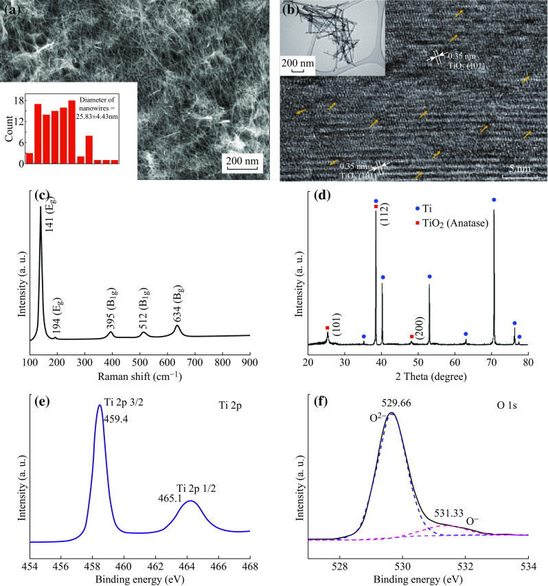
Characterization of TiO2 nanowires. a Top view SEM image (inset, statistical summary of diameters of ~ 100 nanowires); b HRTEM image, yellow arrows indicate the crystalline defects (inset, TEM image of TiO2 nanowires); c Raman spectrum; d XRD results; e Ti 2p XPS spectrum; and f O 1s XPS spectrum
A room-temperature Raman spectrum of TiO2 nanowires in Fig. 1c shows peaks at 141, 194, 395, 512, and 634 cm−1. These peaks are characteristic of the anatase phase. The peaks at 141, 194, and 634 cm−1 are assigned to the E g modes, while the other two peaks at 512 and 395 cm−1 are assigned to the B 1g modes in TiO2 [34]. The XRD characterization results in Fig. 1d further confirm the phase of the TiO2 nanowires, as the peaks of (101), (112), and (200) planes of anatase in agreement with the standard spectrum (JCPDS No. 21-1272). It should be noted that one of the anatase peaks at 38.57° overlapped with the peaks of the Ti foil (JCPDS No. 44-1294).
Moreover, the surface chemical states of the TiO2 nanowires were analyzed by XPS. Figure 1e shows peaks at binding energies of 459.4 and 465.1 eV, which can be assigned to Ti 2p3/2 and 2p1/2, respectively. These are typical XPS spectra of Ti4+ in TiO2. The signal from Ti3+ is too small to be detected. Furthermore, two Gaussian peaks are observed in the fit to the O 1s spectrum (Fig. 1f). The binding energy at 529.66 eV is assigned to the O2– bond in TiO2 while the binding energy at 531.33 eV can be attributed to oxygen vacancies in TiO2 [27]. XPS scans show that the synthesized TiO2 nanowires contain locally distributed oxygen vacancies, in agreement with the high-resolution TEM (HRTEM) result in Fig. 1b.
Electrical Performance Evaluation
Resistive Switching Characteristics
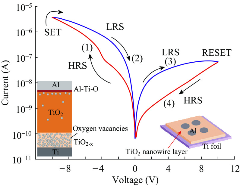
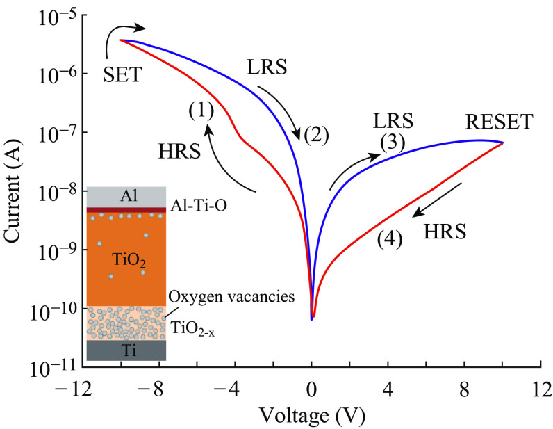
The resistive switching behavior was examined by applying the voltages as follows: 0 V → −10 V → 0 V → 10 V → 0 V with a sweeping rate of 0.1 V s−1. The I–V characteristic curve illustrated in Fig. 2 demonstrates a typical bipolar switching behavior. The Al/TiO2 nanowire networks/Ti device was initially in the high-resistance state (HRS). During the application of the negative sweep from 0 to −10 V, the negative current increased gradually, and the device switched to low-resistance state (LRS, ON state) (SET process). The device maintained the LRS during the forward voltage sweep but switched back to the HRS during the voltage sweep back from 10 to 0 V (RESET process). Notably, the resistive switching behavior is obtained without an initial electroforming process, which was normally required for devices consisting of TiO2 thin films [6, 35, 36]. This is expected to be due to the high concentration of defects (oxygen vacancies) in the TiO2 nanowires after the synthesis process, as seen in the HRTEM image in Fig. 1b and the O 1s XPS spectrum in Fig. 1f. Forming-free resistive switching behavior has also been observed with metal oxide materials containing a large defect concentration [12, 37, 38]. However, some devices require forming treatments, such as hydrogen annealing [39] and Ar+ irradiation [40] to generate an oxygen vacancy layer to enable or enhance the resistive switching characteristics. This electroforming-free characteristic is attractive for ReRAM since it would simplify the memory operation and enable higher density memory devices [41].
Fig. 2.
I–V characteristic curves of the Al/TiO2 nanowire networks/Ti device (inset, schematic diagram of the device in the pristine state)
It should be noted that this resistive switching behavior is quite different from Ref. [17], which shows that Ti/TiO2 film/Al structures display linear I–V characteristic curves due to the Ohmic–Ohmic contact combination. The difference is expected to be ascribed to the reactions at the Ti/TiO2 and Al/TiO2 interfaces during the synthesis of the TiO2 nanowire networks and the deposition of Al layer. In general, the Ti layer is regarded as a chemically reactive contact that will reduce the TiO2 and create a locally high concentration of oxygen vacancies near the Ti/TiO2 interface [19, 42, 43]. The formation reaction of oxygen vacancies is expressed in the Kröger–Vink notation [44] as
| 1 |
where is the oxygen on the TiO2 lattice, and is a positively charged oxygen vacancy. The generation of oxygen vacancies near the interface between Ti and TiO2 nanowires is enhanced during the calcination process due to an increase in the diffusion of Ti atoms into the TiO2 layer at high temperature. Therefore, a nonstoichiometric TiO2-x (x > 0) layer with a high concentration of oxygen vacancies would be formed between the Ti foil and TiO2 nanowires. Oxygen vacancies in TiO2 act as n-type dopants with shallow donor states below the conduction band and would transform the insulating metal oxide into an electrically conductive semiconductor [5, 6]. In addition, oxygen vacancies in TiO2 exhibit higher mobility than metal interstitials at room temperature, so that a number of oxygen vacancies in TiO2 are expected to dominate resistive switching behavior [15]. The distribution of oxygen vacancies in the TiO2 nanowire layer is expected to be uniform above the Ti/TiO2 interface [39]. On the other hand, during the deposition of the Al layer, the high oxygen affinity of Al results in Al reacting with TiO2, forming an interfacial insulating Al–Ti–O layer [1, 18, 45, 46]. Consequently, oxygen vacancies are expected to be generated underneath the interfacial layer according to Eq. 1, although a much smaller concentration of vacancies is expected compared to the Ti/TiO2 interface [6]. These interfaces in the pristine state are illustrated schematically in the inset of Fig. 2. The different concentrations of oxygen vacancies distributed at the Al/TiO2 interface and Ti/TiO2 interface result in asymmetric barriers for charge transport, which plays an important role in the switching behavior of the device.
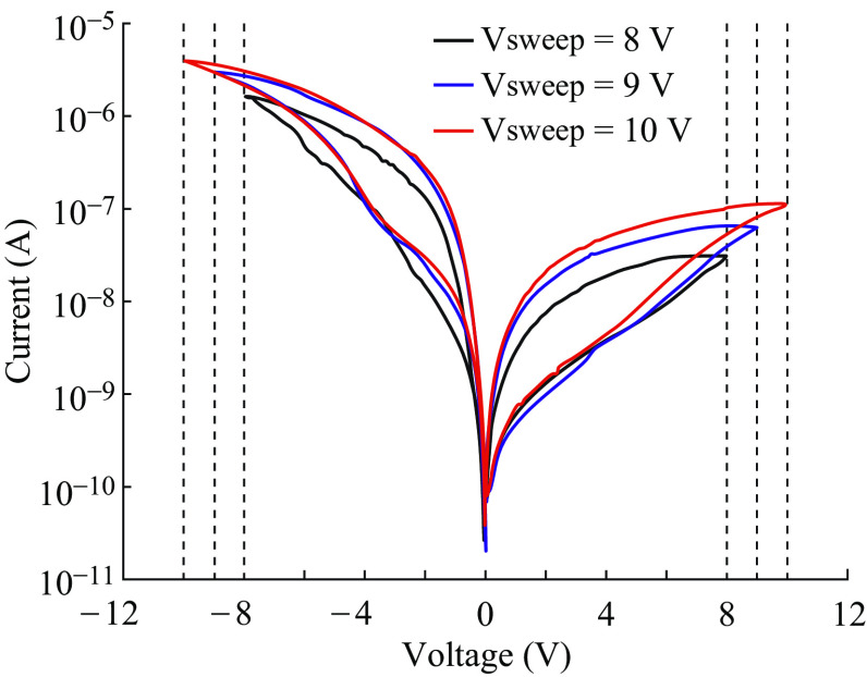
Furthermore, Fig. 3 shows I–V characteristic curves under different sweeping voltages and displays similar bipolar resistive switching behavior in spite of difference in the achieved SET and RESET currents. These results highlight the repeatability of the Al/TiO2 nanowire networks/Ti device. Asymmetrical or self-rectifying resistive switching can be seen in both Figs. 2 and 3. The origin of this self-rectifying property can be attributed to effect of the Al–Ti–O layer on the migration of oxygen vacancies as discussed in the next section.
Fig. 3.
I–V characteristic curves of Al/TiO2 nanowire networks/Ti device under different sweeping voltages
Switching Mechanism Analysis
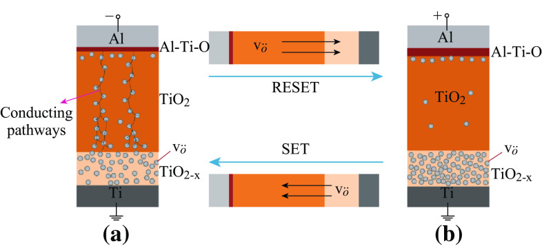
Based on the discussed I–V characteristic results, the resistive switching mechanism of the Al/TiO2 nanowire networks/Ti device is proposed. As explained, the concentration of oxygen vacancies at the Al/TiO2 interface and Ti/TiO2 interface is different. These oxygen vacancies are mobile under external electrical field [47]. When the Al top electrode is under a negative bias, the oxygen vacancies in the pristine state (Fig. 4b) migrate towards the top electrode, forming pathways with high electrical conductivity. It is expected that the geometry of the confined TiO2 nanowire provides a large surface area and a direct pathway for the migration of oxygen vacancies for stable switching behavior [12]. Simultaneously, electrons would be injected from the Al electrode and drift to the bottom Ti electrode. Once one or more conductive pathways are formed from the top electrode to bottom electrode, the device is switched ON, as illustrated in Fig. 4a. Moreover, some oxygen vacancies may accumulate at the Al–Ti–O layer, which functions as an insulating layer to inhibit out-diffusion of oxygen [45]. This insulating layer may play an important role in the switching behavior since the formation and dissociation of this layer is expected to be closely related to the migration of oxygen vacancies under electric field [1, 46]. Under negative bias, the migration of oxygen vacancies to the Al electrode may result in the partial dissolution of this insulating layer, whereas this layer would be widened when the Al top layer is under a positive bias.
Fig. 4.
Schematic illustration of a SET and b RESET process of the Al/TiO2 nanowire networks/Ti device
In the ReSET process, the oxygen vacancies in the TiO2 matrix are repelled towards the bottom electrode, leading to the recovery of a higher concentration of oxygen vacancies near the Ti bottom layer, and widening of the Al–Ti–O layer as oxygen vacancies drift away from this layer [6]. The presence of a potential barrier in the Al/Al–Ti–O interfacial layer would suppress electron tunneling through the interface and inhibit the formation of conducting channels. Conversely, as oxygen vacancies migrate to the top Al electrode under an applied negative bias, the interfacial layer begins to thin, increasing the probability of electron tunneling and enhancing the formation of conductive channels. As a result, the final current flowing at +10 V is much less than that at −10 V. This is characteristic of asymmetrical or self-rectifying resistive switching behavior, as seen in Figs. 2 and 3. To verify the source of the self-rectifying performance, an identical device was measured without the top electrode, that is, the probe tip (which is made of tungsten) is directly in contact with the top surface of the TiO2 nanowire layer. We found the bipolar resistive switching performance existed for the device as well, but no self-rectifying feature was observed.
Further insight into the role of the Al–Ti–O interfacial layer on the resistive switching performance can be obtained by investigating the effect of the thickness of the TiO2 nanowire network. This thickness can be varied by changing the hydrothermal growth time. The effect of different growth times (different thickness) on the I–V characteristics is illustrated in Fig. 5. These data can be compared with those in Fig. 2 which was obtained for a hydrothermal growth time of 20 h. A self-rectifying resistive switching response was also observed for growth time of 4, 12, and 16 h in addition to 20 h, and the rectification ratio diminishes as the growth time is increased. As discussed, the interfacial Al–Ti–O layer plays an important role in determining the asymmetrical response. The relative effect of this component increases with decreasing thickness of the TiO2 nanowire layer so that an increase in growth time to 24 h results in bipolar resistive switching with no obvious self-rectifying feature. The data in Fig. 5a suggests that self-rectifying resistive switching of our Al/TiO2 nanowire networks/Ti could, after further optimization, be used to mitigate sneak-current issues in the crossbar-based integration system for ReRAM devices [8].
Fig. 5.
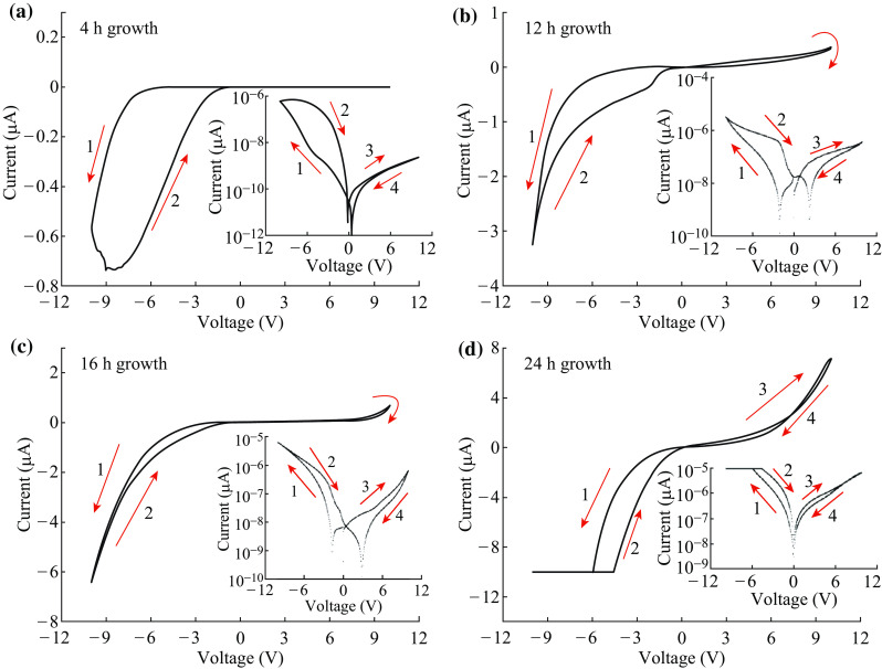
I–V characteristic curves of the Al/TiO2 nanowire networks/Ti device with different thicknesses of the nanowire layers via the control of the hydrothermal growth time. a 4 h growth time, b 12 h growth time, c 16 h growth time, and d 24 h growth time
In order to understand the conduction mechanism of the fabricated Al/TiO2 nanowire networks/Ti device, the I–V curves in Fig. 2 were fitted on a double-logarithmic scale, as shown in Fig. 6. The overall curve is in good agreement with the trap-associated space charge limited current (SCLC) theory [12, 18, 45]. For the positive sweeping (Fig. 6a), the LRS follows an Ohmic conduction with a slope of ~1, which is consistent with the presence of conductive pathways formed by the migration of oxygen vacancies in the device after the SET process [39]. The I–V characteristics in the HRS consist of three regions: the Ohmic region (I–V) with a slope of ~1 at low bias, the Child’s square law region *(I ~ V 2) with a slope of 2.44 at higher bias and a region with rapidly changing current near the RESET point (slope: 4.23). The higher slope (>2) compared with the Child’s law in which the current is proportional to the square of the voltage might be due to the expected variation in thickness of the insulating Al–Ti–O layer. This large slope can also be found in similar ReRAM devices in which Al acts as an electrode [18, 45, 48].
Fig. 6.
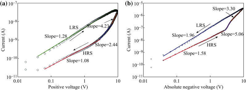
I–V characteristic curves under positive a, and negative b sweeping voltages on a double-logarithmic scale
The I–V characteristic curve for the negative voltage in Fig. 6b also demonstrates SCLC-like behavior but the fitted slope values in different regions are generally larger than those under positive voltage sweeping. This could be due to the concentration gradient of oxygen vacancies that exists in the pristine state (high concentration of vacancies at the bottom Ti/TiO2 interface and low concentration underneath the Al–Ti–O layer), which would lead to diffusion of these oxygen vacancies. The diffusion combined with the drift of the oxygen vacancies under an applied negative bias could lead to accelerated migration of vacancies, resulting in higher slopes when transitioning from the HRS to LRS, as compared to the transition from LRS to HRS under positive sweeping. Furthermore, dissociation of the insulating Al–Ti–O layer due to migration of oxygen vacancies under negative bias also decreases the overall resistance of the device, which would contribute to higher values of the slopes. This SCLC-like behavior for both positive and negative sweeping voltages can also be found with increasing sweeping cycles of the device.
The above analysis indicates that Al/TiO2 nanowire networks/Ti device as fabricated exhibits a similar I–V response and switching mechanism as that seen in devices using a uniform TiO2 layer coated with an Al electrode. Such devices were fabricated by time-consuming and costly reactive sputtering [18] or plasma-enhanced atomic layer deposition [1, 45, 46, 48, 49] processes. Therefore, our results indicate that the TiO2 nanowire networks grown on Ti foil by a single-step hydrothermal process have potential in the application of ReRAM devices.
Endurance and Retention Study
To determine the electrical stability of the fabricated Al/TiO2 nanowire networks/Ti device, an endurance study was performed by applying a cycling sweeping process. The results illustrated in Fig. 7a show that the resistance for the OFF state remains stable beyond 60 cycles, while the resistance for the ON state undergo a fluctuation. Nevertheless, the calculated OFF/ON resistance ratio is around 70, large enough to serve as a feasible memory element in ReRAM. Study of endurance under pulsed operation is planned for future work, together with characterization of the device in relation to stability. Furthermore, a data retention test was performed by examining the resistance change with a reading voltage of 1 V for a long period of time after switching the device to ON and OFF states at −10 and 10 V, respectively. The retention results for the ON and OFF states in Fig. 7b demonstrated no remarkable degradation up to 104 s with a high resistance ratio, confirming the nonvolatile nature of the device. The endurance and retention results emphasize good stability of the fabricated Al/TiO2 nanowire networks/Ti device for future use as ReRAM.
Fig. 7.
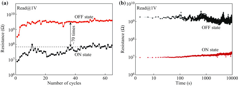
a Endurance and b retention performance of the Al/TiO2 nanowire networks/Ti device
Conclusions
In summary, electroforming-free bipolar resistive switching behavior was successfully demonstrated in TiO2 nanowire networks directly grown on Ti foil by a one-step hydrothermal process. The prepared Al/TiO2 nanowire networks/Ti device exhibited reproducible and stable electrical performance with a high OFF/ON ratio that persisted for up to 104 s. We found that the interaction of Ti foil with the TiO2 nanowires during the synthesis process results in the generation of large density of oxygen vacancies at the Ti/TiO2 interface, which is likely responsible for the forming-free resistive switching behavior. The switching mechanism of the device is proposed to be the migration of oxygen vacancies under electric field. These results provide an easy way to prepare nanowire-based ReRAM devices with good electrical performance.
Acknowledgements
This work was supported by the Natural Sciences and Engineering Research Council (NSERC) of Canada. The financial support of the State Scholarship Fund of China (No. 201506160061) is greatly acknowledged. M. Xiao would like to thank Carmen Andrei from the Canadian Center for Electron Microscopy, McMaster University, for help with TEM.
References
- 1.Jeong HY, Lee JY, Choi S-Y. Interface-engineered amorphous TiO2-based resistive memory devices. Adv. Funct. Mater. 2010;20(22):3912–3917. doi: 10.1002/adfm.201001254. [DOI] [Google Scholar]
- 2.Wang B, Ren T, Chen S, Zhang B, Zhang R, Qi J, Chu S, Huang J, Liu J. Resistive switching in Ga- and Sb-doped ZnO single nanowire devices. J. Mater. Chem. C. 2015;3:11881–11885. doi: 10.1039/C5TC02102B. [DOI] [Google Scholar]
- 3.Oka K, Yanagida T, Nagashima K, Kawai T, Kim JS, Park BH. Resistive-switching memory effects of NiO nanowire/metal junctions. J. Am. Chem. Soc. 2010;132(19):6634–6635. doi: 10.1021/ja101742f. [DOI] [PubMed] [Google Scholar]
- 4.Oka K, Yanagida T, Nagashima K, Kanai M, Kawai T, Kim J-S, Park BH. Spatial nonuniformity in resistive-switching memory effects of NiO. J. Am. Chem. Soc. 2011;133(12):12482–12485. doi: 10.1021/ja206063m. [DOI] [PubMed] [Google Scholar]
- 5.Strukov DB, Snider GS, Stewart DR, Williams RS. The missing memristor found. Nature. 2008;453(7191):80–83. doi: 10.1038/nature06932. [DOI] [PubMed] [Google Scholar]
- 6.Yang JJ, Pickett MD, Li X, Ohlberg DA, Stewart DR, Williams RS. Memristive switching mechanism for metal/oxide/metal nanodevices. Nat. Nanotechnol. 2008;3(7):429–433. doi: 10.1038/nnano.2008.160. [DOI] [PubMed] [Google Scholar]
- 7.Huang C-H, Huang J-S, Lin S-M, Chang W-Y, He J-H, Chueh Y-L. ZnO1-x nanorod arrays/ZnO thin film bilayer structure: from homojunction diode and high-performance memristor to complementary 1D1R application. ACS Nano. 2012;6(9):8407–8414. doi: 10.1021/nn303233r. [DOI] [PubMed] [Google Scholar]
- 8.Liu Z-J, Gan J-Y, Yew T-R. ZnO-based one diode-one resistor device structure for crossbar memory applications. Appl. Phys. Lett. 2012;100(15):153503. doi: 10.1063/1.3701722. [DOI] [Google Scholar]
- 9.Sasaki T, Ueda H, Kanki T, Tanaka H. Electrochemical gating-induced reversible and drastic resistance switching in VO2 nanowires. Sci. Rep. 2015;5:17080. doi: 10.1038/srep17080. [DOI] [PMC free article] [PubMed] [Google Scholar]
- 10.Gao S, Zeng F, Wang M, Wang G, Song C, Pan F. Tuning the switching behavior of binary oxide-based resistive memory devices by inserting an ultra-thin chemically active metal nanolayer: a case study on the Ta2O5–Ta system. Phys. Chem. Chem. Phys. 2015;17(19):12849–12856. doi: 10.1039/C5CP01235J. [DOI] [PubMed] [Google Scholar]
- 11.Lee M-J, Lee CB, Lee D, Lee SR, Chang M, et al. A fast, high-endurance and scalable nonvolatile memory device made from asymmetric Ta2O5-x/TaO2-x bilayer structures. Nat. Mater. 2011;10(8):625–630. doi: 10.1038/nmat3070. [DOI] [PubMed] [Google Scholar]
- 12.Liang KD, Huang CH, Lai CC, Huang JS, Tsai HW, et al. Single CuOx nanowire memristor: forming-free resistive switching behavior. ACS Appl. Mater. Interfaces. 2014;6(19):16537–16544. doi: 10.1021/am502741m. [DOI] [PubMed] [Google Scholar]
- 13.Park K, Lee JS. Flexible resistive switching memory with a Ni/CuO/Ni structure using an electrochemical deposition process. Nanotechnology. 2016;27(12):125203. doi: 10.1088/0957-4484/27/12/125203. [DOI] [PubMed] [Google Scholar]
- 14.Chang T, Jo S-H, Lu W. Short-term memory to long-term memory transition in a nanoscale memristor. ACS Nano. 2011;5(9):7669–7676. doi: 10.1021/nn202983n. [DOI] [PubMed] [Google Scholar]
- 15.K. Szot, M. Rogala, W. Speier, Z. Klusek, A. Besmehn, R. Waser, TiO2-a prototypical memristive material. Nanotechnology 22(25), 254001(2011). doi:10.1088/0957-4484/22/25/254001 [DOI] [PubMed]
- 16.Oh SC, Jung HY, Lee H. Effect of the top electrode materials on the resistive switching characteristics of TiO2 thin film. J. Appl. Phys. 2011;109(12):124511. doi: 10.1063/1.3596576. [DOI] [Google Scholar]
- 17.Hernández-Rodríguez E, Márquez-Herrera A, Zaleta-Alejandre E, Meléndez-Lira M, Cruz Wld, Zapata-Torres M. Effect of electrode type in the resistive switching behaviour of TiO2 thin films. J. Phys D-Appl. Phys. 2013;46(4):045103. doi: 10.1088/0022-3727/46/4/045103. [DOI] [Google Scholar]
- 18.Shao XL, Zhou LW, Yoon KJ, Jiang H, Zhao JS, Zhang KL, Yoo S, Hwang CS. Electronic resistance switching in the Al/TiOx/Al structure for forming-free and area-scalable memory. Nanoscale. 2015;7(25):11063–11074. doi: 10.1039/C4NR06417H. [DOI] [PubMed] [Google Scholar]
- 19.Hu C, McDaniel MD, Posadas A, Demkov AA, Ekerdt JG, Yu ET. Highly controllable and stable quantized conductance and resistive switching mechanism in single-crystal TiO2 resistive memory on silicon. Nano Lett. 2014;14(8):4360–4367. doi: 10.1021/nl501249q. [DOI] [PubMed] [Google Scholar]
- 20.Du Y, Pan H, Wang S, Wu T, Feng YO, Pan J, Wee ATS. Symmetrical negative differential resistance behavior of a resistive switching device. ACS Nano. 2012;6(3):2517–2524. doi: 10.1021/nn204907t. [DOI] [PubMed] [Google Scholar]
- 21.Qingjiang L, Khiat A, Salaoru I, Papavassiliou C, Hui X, Prodromakis T. Memory impedance in TiO2 based metal-insulator-metal devices. Sci. Rep. 2014;4:4522. doi: 10.1038/srep04522. [DOI] [PMC free article] [PubMed] [Google Scholar]
- 22.Jana D, Samanta S, Roy S, Lin YF, Maikap S. Observation of resistive switching memory by reducing device zize in a new Cr/CrOx/TiOx/TiN structure. Nano-Micro Lett. 2015;7(4):392–399. doi: 10.1007/s40820-015-0055-3. [DOI] [PMC free article] [PubMed] [Google Scholar]
- 23.O’Kelly C, Fairfield JA, Boland JJ. A single nanoscale junction with programmable multilevel memory. ACS Nano. 2014;8(11):11724–11729. doi: 10.1021/nn505139m. [DOI] [PubMed] [Google Scholar]
- 24.Lin L, Liu L, Musselman K, Zou G, Duley WW, Zhou YN. Plasmonic-radiation-enhanced metal oxide nanowire heterojunctions for controllable multilevel memory. Adv. Funct. Mater. 2016;26:5979–5986. doi: 10.1002/adfm.201601143. [DOI] [Google Scholar]
- 25.Zhang F, Gan X, Li X, Wu L, Gao X, Zheng R, He Y, Liu X, Yang R. Realization of rectifying and resistive switching behaviors of TiO2 nanorod arrays for nonvolatile memory. Electrochem. Solid-State Lett. 2011;14(10):H422–H425. doi: 10.1149/1.3617442. [DOI] [Google Scholar]
- 26.Senthilkumar V, Kathalingam A, Kannan V, Senthil K, Rhee J-K. Reproducible resistive switching in hydrothermal processed TiO2 nanorod film for non-volatile memory applications. Sens. Actuators A. 2013;194:135–139. doi: 10.1016/j.sna.2013.02.009. [DOI] [Google Scholar]
- 27.Chu D, Younis A, Li S. Direct growth of TiO2 nanotubes on transparent substrates and their resistive switching characteristics. J. Phys D-Appl. Phys. 2012;45(35):355306. doi: 10.1088/0022-3727/45/35/355306. [DOI] [Google Scholar]
- 28.Liu B, Boercker JE, Aydil ES. Oriented single crystalline titanium dioxide nanowires. Nanotechnology. 2008;19(50):505604. doi: 10.1088/0957-4484/19/50/505604. [DOI] [PubMed] [Google Scholar]
- 29.Liao J-Y, Lei B-X, Chen H-Y, Kuang D-B, Su C-Y. Oriented hierarchical single crystalline anatase TiO2 nanowire arrays on Ti-foil substrate for efficient flexible dye-sensitized solar cells. Energy Environ. Sci. 2012;5(2):5750–5757. doi: 10.1039/C1EE02766B. [DOI] [Google Scholar]
- 30.Wu WQ, Rao HS, Xu YF, Wang YF, Su CY, Kuang DB. Hierarchical oriented anatase TiO2 nanostructure arrays on flexible substrate for efficient dye-sensitized solar cells. Sci. Rep. 2013;3:1892. doi: 10.1038/srep01892. [DOI] [PMC free article] [PubMed] [Google Scholar]
- 31.Ren S, Liu W. One-step photochemical deposition of PdAu alloyed nanoparticles on TiO2 nanowires for ultra-sensitive H2 detection. J. Mater. Chem. A. 2016;4(6):2236–2245. doi: 10.1039/C5TA06917C. [DOI] [Google Scholar]
- 32.Huo K, Zhang X, Fu J, Qian G, Xin Y, Zhu B, Ni H, Chu PK. Synthesis and field emission properties of rutile TiO2 nanowires arrays grown directly on a Ti metal self-source substrate. J. Nanosci. Nanotechnol. 2009;9(5):3341–3346. doi: 10.1166/jnn.2009.VC09. [DOI] [PubMed] [Google Scholar]
- 33.Wu Y, Long M, Cai W, Dai S, Chen C, Wu D, Bai J. Preparation of photocatalytic anatase nanowire films by in situ oxidation of titanium plate. Nanotechnology. 2009;20(18):185703. doi: 10.1088/0957-4484/20/18/185703. [DOI] [PubMed] [Google Scholar]
- 34.Ohsaka T, Izumi F, Fujiki Y. Raman spectrum of Anatase, TiO2. J. Raman Spectrosc. 1978;7(6):321–324. doi: 10.1002/jrs.1250070606. [DOI] [Google Scholar]
- 35.Kwon D-H, Kim KM, Jang JH, Jeon JM, Lee MH, et al. Atomic structure of conducting nanofilaments in TiO2 resistive switching memory. Nat. Nanotechnol. 2010;5(2):148–153. doi: 10.1038/nnano.2009.456. [DOI] [PubMed] [Google Scholar]
- 36.Kim KM, Choi BJ, Shin YC, Choi S, Hwang CS. Anode-interface localized filamentary mechanism in resistive switching of TiO2 thin films. Appl. Phys. Lett. 2007;91(1):012907. doi: 10.1063/1.2749846. [DOI] [Google Scholar]
- 37.Wang PC, Li PG, Zhi YS, Guo DY, Pan AQ, Zhan JM, Liu H, Shen JQ, Tang WH. Bias tuning charge-releasing leading to negative differential resistance in amorphous gallium oxide/Nb:SrTiO3 heterostructure. Appl. Phys. Lett. 2015;107(26):262110. doi: 10.1063/1.4939437. [DOI] [Google Scholar]
- 38.Hota MK, Nagaraju DH, Hedhili MN, Alshareef HN. Electroforming free resistive switching memory in two-dimensional VOx nanosheets. Appl. Phys. Lett. 2015;107(16):163106. doi: 10.1063/1.4933335. [DOI] [Google Scholar]
- 39.Sun Y, Yan X, Zheng X, Liu Y, Zhao Y, Shen Y, Liao Q, Zhang Y. High On-Off ratio improvement of ZnO-based forming-free memristor by surface hydrogen annealing. ACS Appl. Mater. Interfaces. 2015;7(13):7382–7388. doi: 10.1021/acsami.5b01080. [DOI] [PubMed] [Google Scholar]
- 40.Barman A, Saini CP, Sarkar PK, Roy A, Satpati B, Kanjilal D, Ghosh SK, Dhar S, Kanjilal A. Probing electron density across Ar+ irradiation-induced self-organized TiO2−x nanochannels for memory application. Appl. Phys. Lett. 2016;108(24):244104. doi: 10.1063/1.4954166. [DOI] [Google Scholar]
- 41.Waser R, Dittmann R, Staikov G, Szot K. Redox-based resistive switching memories- nanoionic mechanisms, prospects, and challenges. Adv. Mater. 2009;21(25–26):2632–2663. doi: 10.1002/adma.200900375. [DOI] [PubMed] [Google Scholar]
- 42.Yang JJ, Strachan JP, Miao F, Zhang M-X, Pickett MD, Yi W, Ohlberg DAA, Medeiros-Ribeiro G, Williams RS. Metal/TiO2 interfaces for memristive switches. Appl. Phys. A. 2011;102(4):785–789. doi: 10.1007/s00339-011-6265-8. [DOI] [Google Scholar]
- 43.Lin C-Y, Wu C-Y, Wu C-Y, Tseng T-Y, Hu C. Modified resistive switching behavior of ZrO2 memory films based on the interface layer formed by using Ti top electrode. J. Appl. Phys. 2007;102(9):094101. doi: 10.1063/1.2802990. [DOI] [Google Scholar]
- 44.Jeong DS, Thomas R, Katiyar RS, Scott JF, Kohlstedt H, Petraru A, Hwang CS. Emerging memories: resistive switching mechanisms and current status. Rep. Prog. Phys. 2012;75(7):076502. doi: 10.1088/0034-4885/75/7/076502. [DOI] [PubMed] [Google Scholar]
- 45.Young Jeong H, Kyu Kim S, Yong Lee J, Choi SY. Role of Interface Reaction on Resistive Switching of Metal/Amorphous TiO2/Al RRAM Devices. J. Electrochem. Soc. 2011;158(10):H979–H982. doi: 10.1149/1.3622295. [DOI] [Google Scholar]
- 46.Jeong HY, Lee JY, Choi S-Y, Kim JW. Microscopic origin of bipolar resistive switching of nanoscale titanium oxide thin films. Appl. Phys. Lett. 2009;95(16):162108. doi: 10.1063/1.3251784. [DOI] [Google Scholar]
- 47.Weibel A, Bouchet R, Knauth P. Electrical properties and defect chemistry of anatase (TiO2) Solid State Ion. 2006;177(3–4):229–236. doi: 10.1016/j.ssi.2005.11.002. [DOI] [Google Scholar]
- 48.Choi BJ, Jeong DS, Kim SK, Rohde C, Choi S, et al. Resistive switching mechanism of TiO2 thin films grown by atomic-layer deposition. J. Appl. Phys. 2005;98(3):033715. doi: 10.1063/1.2001146. [DOI] [Google Scholar]
- 49.Kim S, Jeong HY, Choi S-Y, Choi Y-K. Comprehensive modeling of resistive switching in the Al/TiOx/TiO2/Al heterostructure based on space-charge-limited conduction. Appl. Phys. Lett. 2010;97(3):033508. doi: 10.1063/1.3467461. [DOI] [Google Scholar]


