Abstract
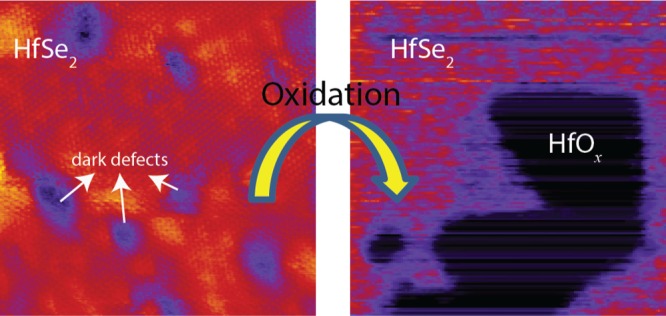
HfSe2 is a very good candidate for a transition metal dichalcogenide-based field-effect transistor owing to its moderate band gap of about 1 eV and its high-κ dielectric native oxide. Unfortunately, the experimentally determined charge carrier mobility is about 3 orders of magnitude lower than the theoretically predicted value. This strong deviation calls for a detailed investigation of the physical and electronic properties of HfSe2. Here, we have studied the structure, density, and density of states of several types of defects that are abundant on the HfSe2 surface using scanning tunneling microscopy and spectroscopy. Compared to MoS2 and WSe2, HfSe2 exhibits similar type of defects, albeit with a substantially higher density of 9 × 1011 cm–2. The most abundant defect is a subsurface defect, which shows up as a dim feature in scanning tunneling microscopy images. These dim dark defects have a substantially larger band gap (1.25 eV) than the pristine surface (1 eV), suggesting a substitution of the Hf atom by another atom. The high density of defects on the HfSe2 surface leads to very low Schottky barrier heights. Conductive atomic force microscopy measurements reveal a very small dependence of the Schottky barrier height on the work function of the metals, suggesting a strong Fermi-level pinning. We attribute the observed Fermi-level pinning (pinning factor ∼0.1) to surface distortions and Se/Hf defects. In addition, we have also studied the HfSe2 surface after the exposure to air by scanning tunneling microscopy and conductive atomic force microscopy. Partly oxidized layers with band gaps of 2 eV and Schottky barrier heights of ∼0.6 eV were readily found on the surface. Our experiments reveal that HfSe2 is very air-sensitive, implying that capping or encapsulating of HfSe2, in order to protect it against oxidation, is a necessity for technological applications.
Introduction
Since the first single-layer MoS2 transistor was fabricated and characterized in 2011,1 it has triggered many scientists to search for transition metal dichalcogenide (TMD)-based applications. Two-dimensional TMDs have been widely studied because of their appealing physical (1T or 2H phase) and electrical (ranging from metallic to half-metallic to semiconducting and even superconducting) properties.2−4 For instance, MoS2 has a thickness-dependent band gap, with a transition of an indirect to direct band gap in case the thickness is reduced to a single layer.5 In addition, superconductivity has been observed in both bulk 1T-MoS26 and pristine 2Ha-MoS2.7 However, compared to Mo or W chalcogenides, HfSe2 has not received much attention. Single-layer HfSe2 is a material with an octahedral structure with an indirect band gap of ∼1 eV,8−10 which makes it an appealing candidate for semiconductor device applications.
HfSe2-based prototype transistors have been realized and investigated by several groups.9,11−13 A high on/off current ratio, exceeding 106, was found, satisfying the requirement for effective switching in digital logic transistors.11 The current density of a trilayer HfSe2 was up to ∼30 μA μm–1.9 Moreover, a phototransistor based on HfSe2 has superior optoelectronic properties with an ultrafast response time and high photocurrent, which is comparable with other TMD phototransistors.12 However, its carrier mobility is rather low, ranging from ∼0.3 to ∼6.5 cm2 V–1 s–1, that is, 3 orders of magnitude lower than the predicted value of ∼3500 cm2 V–1 s–1 at room temperature.14
Besides device optimization, such as the inclusion of dielectric layers and the selection of proper metal contacts, the quality of the material should be also improved in order to obtain properly operating devices. It is known that TMD materials suffer from a large number of intrinsic defects located either in the transition metal layer or in the chalcogenide layer.15−17 Moreover, the air stability of HfSe2 needs to be investigated too. These key issues, that is, intrinsic defects and air stability, have to be considered in order to properly evaluate the application prospects of HfSe2.
Defects often play a significant role in determining the electronic behavior in TMDs.18−23 Intrinsic defects dominate the contact resistance between metal contacts and TMDs19 and can act as scattering centers,20 degrading the charge carrier mobility. Defects are also expected to dominate the surface conductivity of HfSe2, leading to the very low carrier mobilities. It is therefore essential to scrutinize the structural and electronic characteristics of HfSe2 and explore the reasons for the poor device performance. We have used scanning tunneling microscopy and spectroscopy (STM/STS) to study variations in the structure and electronic local density of states (LDOS) of the HfSe2 surface. We have found several types of defects located in either the uppermost Se layer or the Hf layer. Furthermore, we have used conductive atomic force microscopy (C-AFM) to measure the influence of these defects on the Schottky barrier height (SBH) formed with different metal contacts and possible partial Fermi-level pinning effects, following the same approach as in ref (21) for MoS2.
In addition, HfSe2 crystals are not stable against oxidation at ambient conditions, implying this air-sensitive HfSe2 surface is detrimental for many applications. Mirabelli et al.24 found a preferential reaction of oxygen with the Hf atoms rather than with the Se atoms, leading to the formation of a HfO2 layer. In principle, the poor air stability of HfSe2 should limit its application in electronic devices. However, HfO2 is a high-κ dielectric oxide, which has been frequently used as a top gate layer for field-effect transistors.1,25 In particular, the native HfO2 layer can effectively suppress the interfacial charge trap states at the HfSe2/HfO2 interface, which is very beneficial for device performance.9 Therefore, it is important to properly understand the oxidation of HfSe2. Unlike earlier Raman and X-ray photoelectron spectroscopy studies,8,13,24 the combination of STM and C-AFM allows us to study the oxidation dynamics and evolution of the electrical properties of HfSe2 with a high spatial resolution.
Experimental Methods
The HfSe2 crystal was purchased from HQ Graphene (Groningen, The Netherlands). The samples were cleaned by mechanical exfoliation and subsequently transferred to a vacuum system as soon as possible for STM and C-AFM measurements. All the STM/STS data were obtained by room-temperature scanning tunneling microscopy (Omicron STM1). The base pressure of the ultrahigh vacuum system is 3 × 10–11 mbar. To obtain I(V) signals by AFM, we applied the bias voltages between the conductive tip (grounded) and the HfSe2 surface to read out the current values. Different conductive tips, including the Pt tips, the PtSi tips, and the n-type Si tips, were used for the measurements. The resonance frequency is 4.5, 15, and 160 kHz for the Pt, PtSi, and n-type Si tips, respectively.
Results and Discussion
Surface Topography and Local Electronic Properties
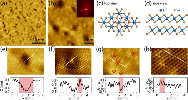
Because of the poor air instability of HfSe2, the mechanical exfoliation was performed in situ in the load lock of the STM system at a base pressure of 1 × 10⁻⁸ mbar. The freshly cleaved sample was then transferred to the main chamber of the STM for imaging. Figure 1a shows a large-scale STM topography image of the freshly cleaved HfSe2 surface. Two different locations across the crystal surface are also recorded in Figure S1, marked as location I and location II. It is clear that the surface of HfSe2 is inhomogeneous, displaying a large number of defects. The density of these defects across the whole sample is about 9 × 10–11 cm–2, which is substantially higher than the defect densities of MoS2 or WSe2,26,27 (see the Supporting Information Figure S2). Such a high density of defects makes it very difficult to find nanometer-sized defect-free regions. By zooming in at parts where the surface structure is still intact, we have acquired the atomic lattice of the surface, as shown in Figure 1b. The lattice constant, as extracted from the images, is 0.378 nm (see the inset in Figure 1b for a fast Fourier transform). This value is in good agreement with the previously reported lattice constant.28Figure 1c,d shows the structural model of bilayer HfSe2. The interlayer distance of the HfSe2 crystal is ∼0.614 nm.29 The single-layer HfSe2 is constituted of a top-Se, center-Hf, and bottom-Se atom layer. These three atom layers acquire an octahedral configuration. In our atomically resolved STM images, only the top-Se atom layer is observed. The unit cell formed by the nearest four neighbor Se atoms corresponds to the red dashed contour marked in the top view of the structural model.
Figure 1.
(a) Large-scale STM topography image on the HfSe2 crystal (100 nm × 100 nm; It = 0.6 nA, Vs = −0.3 V). (b) Atomically resolved image of the HfSe2 surface (20 nm × 20 nm; It = 0.6 nA, Vs = −0.4 V). The inset is the corresponding fast Fourier transform image. (c) Top-view and (d) side-view sketches of a bilayer HfSe2. (e–h) Atomic-scale STM images and line scans of defects on HfSe2 (It = 0.6 nA, Vs = −0.4 V).
The most abundant defects are shown in Figure 1e−g, which are dark defects, bright defects, and atom vacancies. The dark defect in Figure 1e has a depth measured by the line profile of around 0.3 nm. Depending on the defect position and sample bias voltage, the height of this depression varies from around 0.1 to 0.8 nm, as described in detail in the Supporting Information. It is worth noting that three types of dark defects have been identified based on their topographical features: (1) a very dark holelike defect with the depression depth of ≥0.7 nm, (2) a less dark defect with the depression depth ranging from 0.5 to 0.7 nm, and (3) a dim dark defect with a visible continuous lattice periodicity and the depression depth of ≤0.5 nm (see the Supporting Information, Figure S4). The third type of defects (dim dark) has a density of 5 × 1011 cm–2. Defects with a similar appearance are also reported to exist on other TMD crystals, either on pristine surfaces or after ion bombardment.26,27,30−32 Since our HfSe2 sample was only treated with scotch-tape cleavage before scanning, the ion-bombardment-induced defects can be ignored here. The dark defects have been interpreted to be caused by poor growth conditions. Its appearance is the result of electron depletion caused by the Coulomb repulsive potential around the Se atom complex or the acceptor impurity near the surface.27,33 The continuation of the lattice periodicity suggests that this type of feature is due to the absence of a Se atom.
In addition to these abundant dark defects, we have found several other types of defects on the surface. Figure 1f presents a hillocklike defect with a density of ∼2.5 × 1011 cm–2, probably caused by an adatom. The adatom could be for instance a Se atom or another impurity atom such as Li, Na, K, and Re.32,34 Moreover, several single-atom vacancies are also found, as shown in Figure 1g. The corresponding cross section reveals the absence of an atom in the lattice. Such single-atom vacancy has a density of ∼0.5 × 1011 cm–2. We also report a new type of defect with a triangular shape, shown in Figure 1h. It has a similar appearance as the 3 × 3 charge density wave superlattice observed in NbSe2.35 Since the charge density wave transition temperature of HfSe2 is rather low, we can exclude this interpretation here. It has been shown that HfSe2 is a suitable host material for extrinsic dopant atoms,36 suggesting that the bright defects might be a result of the intercalation of impurities.
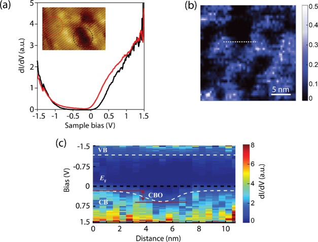
In the following section, we investigate the influence of the aforementioned defects on the local density of states of the HfSe2 surface using scanning tunneling spectroscopy (STS). Figure 2a shows the local tunneling conductance (dI/dV) spectra taken at the red and black dashed circles, which correspond to the dim dark defect and the pristine region, respectively. The conductance spectra for the bright defect in Figure 1f is also displayed in the Supporting Information (Figure S5). The dI/dV spectra, which are proportional to the electronic local density of states (LDOS) near the Fermi level for small sample biases, are obtained by numerical differentiating 3600 current–voltage curves recorded in a 60 × 60 grid. Both recorded curves exhibit an n-type semiconducting behavior, in good agreement with previous STM and electrical transport measurements.8,11,12 The Fermi level is much closer to the conduction band (CB) than to the valence band (VB) because of the strong doping from the Se atom vacancies in the crystal. The sharp increases in the dI/dV spectra correspond to the CB and VB band edges. The band gap as extracted from these curves is about 1 eV for the pristine HfSe2 surface and 1.25 eV for the dim dark defects. In addition, the dI/dV map in Figure 2b illustrates the large fluctuation of the LDOS of HfSe2, induced by the presence of the high density of intrinsic defects on the HfSe2 surface. The STM topography image simultaneously recorded with the dI/dV map is shown in the Supporting Information, Figure S6. The dI/dV spectra along the dashed white line in Figure 2b are taken to determine the real space band profiles. As shown in Figure 2c, there is a conduction band offset between the conduction band minima of the defect and the pristine surface that amounts to ∼0.2 eV. In principle, S or Se atom vacancies in TMDs can lead to enhancement of the LDOS in the conduction band because of the broken covalent bonds, leading to a reduction of the CBM.37,38 In contrast, we observe an upward shift of the CBM. The atomically resolved STM topography images of the dim dark defects (shown in Figure 1e) show an intact lattice periodicity, indicating that these defects are buried under the surface. Therefore, the possible mechanism for the shift of the CBM might involve substitutional dopants, like Mo, W, or Sn atoms. The presence of these substitutional atoms could be caused by the crystal growth process. The brighter LDOS signal in Figure 2b is most probably related to the presence of triangular defects; however, their considerable smaller size does not allow for accurately capturing their influence on the surface.
Figure 2.
Scanning tunneling spectroscopy results of the HfSe2 surface: (a) dI/dV spectra at different regions. Inset: STM image showing the locations where the spectroscopy data were taken from. (b) dI/dV map of HfSe2 (100 nm × 100 nm; It = 0.6 nA, Vs = −0.3 V). (c) Color-coded rendering of the real space imaging of the band profile plotted in terms of dI/dV taken along the dashed white line in (b).
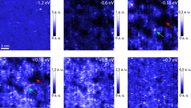
Spatial maps of the LDOS recorded at various energies on the same HfSe2 surface location as discussed in Figure 2b are shown in Figure 3. These dI/dV maps are recorded simultaneously with the topographic image. The dark (red arrows) and bright (green arrows) regions correspond to the dark defects and the pristine areas, respectively. In the vicinity of the Fermi level (−0.15 eV ≤ E ≤ 0.15 eV), large inhomogeneities of the LDOS are clearly observed. The pristine HfSe2 has a higher conductance, which is in accordance with the dI/dV curves shown in Figure 2a. For energies far away from the Fermi level, the distribution of the LDOS becomes more and more uniform.
Figure 3.
Spatially resolved density-of-state maps obtained on the HfSe2 surface at different energies (20 nm × 20 nm, It = 0.5 nA), taken at −1.2, −0.6, −0.15, +0.15, +0.3, and +0.7 V.
Schottky Barrier Height and Fermi-Level Pinning of the HfSe2 Crystal
Owing to the moderate band gap of around 1 eV, which is comparable to silicon, HfSe2-based field-effect transistors have been investigated. However, the mobility obtained in transport measurements is much lower than the theoretically predicted one.9,11,13 The following reasons for the low charge carrier mobility have been put forward. Firstly, the high anisotropic electrical resistivity of HfSe2 can suppress the vertical charge transport in the Ohmic regime. Secondly, the barrier at nonideal Ohmic contacts induces large contact resistances and further limits the mobility. Thirdly, the environmental instability of HfSe2 can cause degradation of the device. In addition, the existence of possible interfacial scattering and interlayer resistance could be also responsible for the low charge carrier mobility. Although a slow decay time of photocurrent in Au-contacted HfSe2 phototransistor was shown to be correlated to defects and charge impurity states,12 the effect of defects on the charge transport of HfSe2 has not yet been studied. In our STM images, we have confirmed the high density of these defects and impurities. The strong influence of the dark defects in the LDOS indicates local variations in electrical contacts.
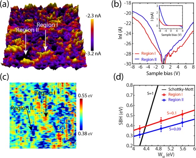
Since a C-AFM tip can be used as a metal nanocontact to measure simultaneously the topography image and I(V) curves, it is possible to make a metal–semiconductor (tip-HfSe2) junction and obtain information on the variation in electrical resistance and contact properties induced by defects on the HfSe2. Figure 4a shows the current map recorded with C-AFM using a highly n-doped Si tip with a work function of about 4.2 eV and a radius of curvature of 2 nm. The inhomogeneous current distribution is consistent with STM topography images. Moreover, voltage-dependent current spectra are recorded in a 128 × 128 grid fashion; the average curves recorded in region I and region II are shown in Figure 4b. We find different charge transport characteristics in region I (red line) and region II (blue line), with region II being much more conductive than region I, especially in the negative sample bias regime (see inset in Figure 4b). Furthermore, the I(V) traces reveal a rectifying behavior with an n-type Schottky barrier. The observation of an n-type Schottky barrier is reminiscent of the n-type doping of the HfSe2 surface. To understand the difference between region I and region II, we have considered thermionic emission as the main transport process. The thermionic emission current I is given by
| 1 |
with
| 2 |
where I0 is the saturation current, V is the applied bias voltage, q is the electron charge, and T is the sample temperature. A is the AFM tip contact area, calculated using the Hertz model.39 κB and A* are the Boltzmann constant and the Richardson constant, respectively. Then, the ideality factor (η) and the Schottky barrier height (ΦB) are obtained by
| 3 |
and
| 4 |
The calculated Schottky barrier height map is shown in Figure 4c; two distinct regions matching region I and region II of the current image are observed, with region I having a larger ΦB than region II. In the map, the highest barrier height is about 0.55 eV, while the lowest one is around 0.38 eV. Combined with the STS results of Figure 2, we assign region I to be a defect-dominated area. In principle, the Schottky barrier height expected from the Schottky–Mott rule should be ∼0.2 eV according to the following equation
| 5 |
The work function Wm of the tip is around 4.2 eV, and the electron affinity χ of the HfSe2 is 4.0 eV.8 The measured barrier height is larger than the expected value by about 0.18–0.35 eV. We attribute this discrepancy to partial Fermi-level pinning. The difference in the ΦB between region I and region II can be understood by the observed difference in the location of the CBM at the two regions (see the STM/STS measurements). The lower CBM (by about 0.2 eV) in region II leads to a smaller barrier height as compared to region I. Moreover, the ideality factors obtained in both regions are between 2 and 4, indicating that thermionic emission is not the sole contributor to the current, but tunneling across the barrier also plays a role.
Figure 4.
(a) Current image (600 nm × 600 nm) of the HfSe2 recorded with C-AFM at a sample bias of 4.7 V. A highly doped Si tip (work function 4.2 eV) has been used. (b) Semilogarithmic contact I(V) curves for region I and region II, as indicated in panel (a). Inset: the corresponding contact I(V) curves. (c) Extracted Schottky barrier height (SBH) map (200 nm × 200 nm) of the surface extracted from I(V) curves, as shown in panel (b). The apparent SBH variations are attributed to the presence of defects on the sample. (d) The Schottky barrier heights of region I (red) and region II (blue) as a function of the tip’s work functions (Wm). The pinning factor S is extracted using eq 6. The black line refers to the standard Schottky–Mott rule (see eq 5).
To investigate the partial Fermi-level effect, we have investigated the charge transport characteristics for tips of different work functions (PtSi of 4.8 eV and Pt of 5.6 eV). The ΦB determined at the two regions for each tip are then plotted as a function of the work function, Figure 4d. The pinning factor is then quantified by the slope S of the curve and given by
| 6 |
here, S takes values between 0 and 1. S = 1 indicates an unpinned interface and the Schottky–Mott rule is fully applicable. For S = 0, the ΦB is independent of the metal work function and the Fermi level is fully pinned. For S between 0 and 1, partial Fermi-level pinning occurs. Here, we found that in region I S is equal to 0.1, while in region II S is equal to 0.09; both of these values signify a strong Fermi-level pinning. A similar behavior has also been observed in metal/MoS2.40,41 Two mechanisms are suggested for the pinning effect in HfSe2. Firstly, distortion of the crystal surface to a large extent results in a notable charge redistribution at the interface between HfSe2 and the contact metal. This can reduce the width of Schottky barrier and enhance the orbital overlap, which could then cause the weak dependence of Wm on ΦB. Secondly, the Se atom vacancies on the HfSe2 surface (see Figure 1g) that act as metallic defects can induce the formation of additional gap states and subsequently strengthen the Fermi-level pinning.
Effect of Oxidation on HfSe2 Surface
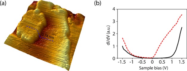
The oxidation of the HfSe2 crystal was first investigated by STM. The three-dimensional (3D) STM topography with a size of 25 nm × 25 nm in Figure 5a presents the HfSe2 surface after 2 days of air exposure. Small flakes with thickness of ∼0.74 nm are readily found on the surface, that is, a value about 0.13 nm larger than the interlayer distance of HfSe2. The surface of the material appears to be much rougher than the freshly cleaved surface. Because of this roughness, atomic-resolution imaging of the crystal’s lattice was not possible. The dI/dV spectra recorded on the pristine and air-exposed HfSe2 surfaces are shown in Figure 5b. The band gap of the air-exposed surface as measured by STS is about 2 eV, which is almost 2 times larger than that of HfSe2. However, the expected band gap of fully oxidized HfO2 is about 5.8 eV.42 This difference suggests that the outermost HfSe2 layer is only partly oxidized and some of the Hf–Se bonds are still preserved.
Figure 5.
(a) Three-dimensional (3D) image of HfSe2 surface after air exposure for 2 days. The blue dashed line profiles the flake height, It = 0.6 nA, Vs = −2.5 V; (b) dI/dV spectra of the oxidized surface (black curve) and pristine HfSe2 (red dashed curve) measured with the same STM tip, It = 0.4 nA, Vs = −1.5 V.
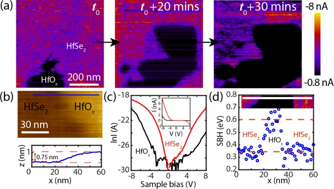
The air stability of HfSe2 was also investigated with C-AFM. In contrast to the ultrahigh vacuum measurements in the STM experiments, the C-AFM measurements were performed in a very low humidity-N2 environment to exclude the influence of water.43 The sample, however, is still exposed to a certain amount of oxygen, allowing us to study in situ the oxidation dynamics of the uppermost HfSe2 layers. Figure 6a shows the time-dependent oxidation process of HfSe2 during a C-AFM measurement. At t0, a small oxidized area was detected at the bottom side of the image by the distinct current intensity, which was 1 order of magnitude lower than that of the pristine surface. After 20 min of scanning of the same region, the oxidized part has spread along all directions, as shown in the second panel of Figure 6a. At t0 + 30 min, the oxidized region occupies more than half of the image. The height of the HfOx flake was measured to be around 0.75 nm, as shown in Figure 6b, in line with the STM result. The current–voltage characteristics averaged from several curves at the pristine and oxidized regions are shown in Figure 6c. As compared to the pristine HfSe2, the oxidized regions are significantly less conductive most probably due to the larger band gap of these regions. The Schottky barrier height of this HfOx layer is determined to be ∼0.61 eV, that is, about 44% larger than that of the unoxidized HfSe2 surface. More importantly, the ideality factor across these two regions has increased from approximately 4 at the unoxidized region to about 20 at the oxidized region. This huge increase in the ideality factor suggests that the current is not solely due to thermionic emission, but that also tunneling plays an important role. To this regard, the oxidized upper flake may act as a tunneling barrier. The measured structural and electrical variations confirm the air sensitivity of HfSe2. HfSe2-based devices operated at ambient conditions will require the use of a protective coating layer in order to avoid oxidation. Another approach is to use the uppermost layer as a dielectric layer; complete oxidation of the uppermost layer is expected to slow down the oxidation of the underlying layers. To that extent, new device architectures need to be considered to account for the effects observed here.
Figure 6.
(a) Oxidation evolution of HfSe2 as measured with C-AFM, which was taken at to, to + 20 min, and to + 30 min. The sample bias is 4.7 V. (b) AFM topography of the transition between an unoxidized and an oxidized region. The blue line shows the apparent height of the HfOx layer. (c) Semilogarithmic contact I(V) curves for HfSe2 and HfOx. Inset: the corresponding contact I(V) curves. (d) Schottky barrier height cross section showing a HfSe2–HfOx–HfSe2 transition.
Conclusions
In summary, HfSe2 crystal surface has been investigated in detail by STM and C-AFM. Atomically resolved STM images of the surface lattice structure demonstrate a high density of intrinsic defects, located both in the Se layer and in the Hf layer. The surface distortion and high density of defects indicate a very poor quality of the HfSe2 crystal, detrimental for many device applications. This poor quality most probably explains the low carrier mobilities found in HfSe2-based field-effect transistors. A prominent defect, with a dim dark appearance localized at the Hf layer with a density of 5 × 1011 cm–2, locally increases the band gap by about 25%, changing it from 1 to 1.25 eV. Moreover, the presence of defects reduces the local barrier height with metal contacts. Furthermore, the small dependence of the measured barrier height on the metal’s work function indicates partial Fermi-level pinning. We have also investigated the oxidation dynamics of HfSe2. After exposure of the crystal to ambient conditions, we find that oxidized layers grow fast and have a band gap of ∼2 eV. The large increase of the Schottky barrier height and ideality factor of the oxidized parts when contacting with a metal tip confirms our interpretation. Therefore, in order to obtain the predicted performance for HfSe2-based electronic devices, the influence of defects and oxidation has to be well controlled or eliminated.
Acknowledgments
This work is part of the research program on 2D semiconductor crystals with project number FV157-TWOD07, which is financed by the Netherlands Organization for Scientific Research (NWO). Q.Y. thanks the China Scholarship Council for financial support.
Supporting Information Available
The Supporting Information is available free of charge on the ACS Publications website at DOI: 10.1021/acs.jpcc.8b08713.
STM topography images of two different regions across the HfSe2 sample (Figure S1); STM topography images of three different TMD surfaces (Figure S2); height of the depression for dark defects (Figure S3); types of dark defects (Figure S4); STS of the bright defect, dark defect, and pristine surface (Figure S5); STM topography image and grid I−V map recorded at the same time (Figure S6) (PDF)
The authors declare no competing financial interest.
Supplementary Material
References
- Radisavljevic B.; Radenovic A.; Brivio J.; Giacometti V.; Kis A. Single-Layer MoS2 Transistors. Nat. Nanotechnol. 2011, 6, 147–150. 10.1038/nnano.2010.279. [DOI] [PubMed] [Google Scholar]
- Butler S. Z.; Hollen S. M.; Cao L.; Cui Y.; Gupta J. A.; Gutierrez H. R.; Heinz T. F.; Hong S. S.; Huang J.; Ismach A. F.; et al. Progress, Challenges, and Opportunities in Two-Dimensional Materials Beyond Graphene. ACS Nano 2013, 7, 2898–2926. 10.1021/nn400280c. [DOI] [PubMed] [Google Scholar]
- Jariwala D.; Sangwan V. K.; Lauhon L. J.; Marks T. J.; Hersam M. C. Emerging Device Applications for Semiconducting Two-Dimensional Transition Metal Dichalcogenides. ACS Nano 2014, 8, 1102–1120. 10.1021/nn500064s. [DOI] [PubMed] [Google Scholar]
- Duong D. L.; Yun S. J.; Lee Y. H. van der Waals Layered Materials: Opportunities and Challenges. ACS Nano 2017, 11, 11803–11830. 10.1021/acsnano.7b07436. [DOI] [PubMed] [Google Scholar]
- Splendiani A.; Sun L.; Zhang Y.; Li T.; Kim J.; Chim C.; Galli G.; Wang F. Emerging Photoluminescence in Monolayer MoS2. Nano Lett. 2010, 10, 1271–1275. 10.1021/nl903868w. [DOI] [PubMed] [Google Scholar]
- Fang Y.; Pan J.; He J.; Luo R.; Wang D.; Che X.; Bu K.; Zhao W.; Liu P.; Mu G.; Zhang H.; Lin T.; Huang F. Structure Re-Determination and Superconductivity Observation of Bulk 1T MoS2. Angew. Chem. 2018, 130, 1246–1249. 10.1002/ange.201710512. [DOI] [PubMed] [Google Scholar]
- Chi Z.; Chen X.; Yen F.; Peng F.; Zhou Y.; Zhu J.; Zhang Y.; Liu X.; Lin C.; Chu S.; Li Y.; Zhao J.; Kagayama T.; Ma Y.; Yang Z. Superconductivity in Pristine 2Ha-MoS2 at Ultrahigh Pressure. Phys. Rev. Lett. 2018, 120, 037002 10.1103/PhysRevLett.120.037002. [DOI] [PubMed] [Google Scholar]
- Yue R.; Barton A. T.; Zhu H.; Azcatl A.; Pena L. F.; Wang J.; Peng X.; Lu N.; Cheng L.; Addou R.; et al. HfSe2 Thin Films: 2D Transition Metal Dichalcogenides Grown by Molecular Beam Epitaxy. ACS Nano 2015, 9, 474–480. 10.1021/nn5056496. [DOI] [PubMed] [Google Scholar]
- Mleczko M. J.; Zhang C.; Lee H. R.; Kuo H.; Magyari-Kope B.; Moore R. G.; Shen Z.; Fisher I. R.; Nishi Y.; Pop E. Pop. HfSe2 and ZrSe2: Two-Dimensional Semiconductors with Native High-κ Oxides. Sci. Adv. 2017, 3, e1700481 10.1126/sciadv.1700481. [DOI] [PMC free article] [PubMed] [Google Scholar]
- Rasmussen F. A.; Thygesen K. S. Computational 2D Materials Database: Electronic Structure of Transition-Metal Dichalcogenides and Oxides. J. Phys. Chem. C 2015, 119, 13169–13183. 10.1021/acs.jpcc.5b02950. [DOI] [Google Scholar]
- Kang M.; Rathi S.; Lee I.; Lim D.; Wang J.; Li L.; Khan M. A.; Kim G. Electrical Characterization of Multilayer HfSe2 Field-Effect Transistors on SiO2 Substrate. Appl. Phys. Lett. 2015, 106, 143108 10.1063/1.4917458. [DOI] [Google Scholar]
- Yin L.; Xu K.; Wen Y.; Wang Z.; Huang Y.; Wang F.; Shifa T. A.; Cheng R.; Ma H.; He J. Ultrafast and Ultrasensitive Phototransistors Based on Few-Layered HfSe2. Appl. Phys. Lett. 2016, 109, 213105 10.1063/1.4968808. [DOI] [Google Scholar]
- Kang M.; Rathi S.; Lee I.; Li L.; Khan M. A.; Lim D.; Lee Y.; Park J.; Yun S. J.; Youn D.; Jun C.; Kim G. Tunable Electrical Properties of Multilayer HfSe2 Field Effect Transistors by Oxygen Plasma Treatment. Nanoscale 2017, 9, 1645–1652. 10.1039/C6NR08467B. [DOI] [PubMed] [Google Scholar]
- Zhang W.; Huang Z.; Zhang W.; Li Y. Two-Dimensional Semiconductors with Possible High Room Temperature Mobility. Nano Res. 2014, 7, 1731–1737. 10.1007/s12274-014-0532-x. [DOI] [Google Scholar]
- Zhou W.; Zou X.; Najmaei S.; Liu Z.; Shi Y.; Kong J.; Lou J.; Ajayan P. M.; Yakobson B. I.; Idrobo J. Intrinsic Structural Defects in Monolayer Molybdenum Disulfide. Nano Lett. 2013, 13, 2615–2622. 10.1021/nl4007479. [DOI] [PubMed] [Google Scholar]
- Liu H.; Zheng H.; Yang F.; Jiao L.; Chen J.; Ho W.; Gao C.; Jia J.; Xie M. Line and Point Defects in MoSe2 Bilayer Studied by Scanning Tunneling Microscopy and Spectroscopy. ACS Nano 2015, 9, 6619–6625. 10.1021/acsnano.5b02789. [DOI] [PubMed] [Google Scholar]
- Zhang S.; Wang C.; Li M.; Huang D.; Li L.; Ji W.; Wu S. Defect Structure of Localized Excitons in a WSe2 Monolayer. Phys. Rev. Lett. 2017, 119, 046101 10.1103/PhysRevLett.119.046101. [DOI] [PubMed] [Google Scholar]
- Wu Z.; Luo Z.; Shen Y.; Zhao W.; Wang W.; Nan H.; Guo X.; Sun L.; Wang X.; You Y.; Ni Z. Defects as a Factor Limiting Carrier Mobility in WSe2: A Spectroscopic Investigation. Nano Res. 2016, 9, 3622–3631. 10.1007/s12274-016-1232-5. [DOI] [Google Scholar]
- McDonnell S.; Addou R.; Buie C.; Wallace R. M.; Hinkle C. L. Defect-Dominated Doping and Contact Resistance in MoS2. ACS Nano 2014, 8, 2880–2888. 10.1021/nn500044q. [DOI] [PubMed] [Google Scholar]
- Liu X.; Balla I.; Bergeron H.; Hersam M. C. Point Defects and Grain Boundaries in Rotationally Commensurate MoS2 on Epitaxial Graphene. J. Phys. Chem. C 2016, 120, 20798–20805. 10.1021/acs.jpcc.6b02073. [DOI] [Google Scholar]
- Bampoulis P.; Bremen R. V.; Yao Q.; Poelsema B.; Zandvliet H. J. W.; Sotthewes K. Defect Dominated Charge Transport and Fermi Level Pinning in MoS2/Metal Contacts. ACS Appl. Mater. Interfaces 2017, 9, 19278–19286. 10.1021/acsami.7b02739. [DOI] [PMC free article] [PubMed] [Google Scholar]
- Ghorbani-Asl M.; Enyashin A. N.; Kuc A.; Seifert G.; Heine T. Defect-Induced Conductivity Anisotropy in MoS2 Monolayers. Phys. Rev. B 2013, 88, 245440 10.1103/PhysRevB.88.245440. [DOI] [Google Scholar]
- Lin Z.; Carvalho B. R.; Kahn E.; Lv R.; Rao R.; Terrones H.; Pimenta M. A.; Terrones M. Defect engineering of two-dimensional transition metal dichalcogenides. 2D Mater. 2016, 3, 022002 10.1088/2053-1583/3/2/022002. [DOI] [Google Scholar]
- Mirabelli G.; McGeough C.; Schmidt M.; McCarthy E. K.; Monaghan S.; Povey I. M.; McCarthy M.; Gity F.; Nagle R.; Hughes G.; Cafolla A.; Hurley P. K.; Duffy R. Air Sensitivity of MoS2, MoSe2, MoTe2, HfS2, and HfSe2. J. Appl. Phys. 2016, 120, 125102 10.1063/1.4963290. [DOI] [Google Scholar]
- Zou K.; Hong X.; Keefer D.; Zhu J. Deposition of High-Quality HfO2 on Graphene and the Effect of Remote Oxide Phonon Scattering. Phys. Rev. Lett. 2010, 105, 126601 10.1103/PhysRevLett.105.126601. [DOI] [PubMed] [Google Scholar]
- Addou R.; Colombo L.; Wallace R. M. Surface Defects on Natural MoS2. ACS Appl. Mater. Interfaces 2015, 7, 11921–11929. 10.1021/acsami.5b01778. [DOI] [PubMed] [Google Scholar]
- Addou R.; Wallace R. M. Surface Analysis of WSe2 Crystals: Spatial and Electronic Variability. ACS Appl. Mater. Interfaces 2016, 8, 26400–26406. 10.1021/acsami.6b08847. [DOI] [PubMed] [Google Scholar]
- Lucovsky G.; White R. M.; et al. Infrared-Reflectance Spectra of Layered Group-IV and Group-VI Transition-Metal Dichalcogenides. Phys. Rev. B 1973, 7, 3859–3870. 10.1103/PhysRevB.7.3859. [DOI] [Google Scholar]
- Schimmel T.; Fuchs H.; Sander R.; Lux-Steiner M. Atomically Resolved STM Imaging of Ion-Bombarded WSe2. Ultramicroscopy 1992, 42–44, 683–688. 10.1016/0304-3991(92)90342-H. [DOI] [Google Scholar]
- Matthes T. W.; Sommerhalter C.; Rettenberger A.; Bruker P.; Boneberg J.; Lux-Steiner M. C.; Leiderer P. Imaging of dopants in surface and sub-surface layers of the transition metal dichalcogenides WS2 and WSe2 by scanning tunneling microscopy. Appl. Phys. A: Mater. Sci. Process. 1998, 66, S1007–S1011. [Google Scholar]
- Murata H.; Kataoka K.; Koma A. Scanning Tunneling Microscope Images of Locally Modulated Structures in Layered Materials, MoS2(0001) and MoSe2(0001), Induced by Impurity Atoms. Surf. Sci. 2001, 478, 131–144. 10.1016/S0039-6028(01)00904-9. [DOI] [Google Scholar]
- Inoue A.; Komori T.; Shudo K. Atomic-Scale Structures and Electronic States of Defects on Ar+-Ion Irradiated MoS2. J. Electron Spectrosc. Relat. Phenom. 2013, 189, 11–18. 10.1016/j.elspec.2012.12.005. [DOI] [Google Scholar]
- Kobayashi K. Scattering Theory of Subsurface Impurities Observed in Scanning Tunneling Microscopy. Phys. Rev. B 1996, 54, 17029 10.1103/PhysRevB.54.17029. [DOI] [PubMed] [Google Scholar]
- Whangbo M. H.; Ren J.; Magonov S. N.; Bengel H.; Parkinson B. A.; Suna A. On the Correlation Between the Scanning Tunneling Microscopy Image Imperfections and Point Defects of Layered Chalcogenides 2H-MX2 (M = Mo, W; X = S, Se). Surf. Sci. 1995, 326, 311–326. 10.1016/0039-6028(94)00800-0. [DOI] [Google Scholar]
- Ugeda M. M.; Bradley A. J.; Zhang Y.; Onishi S.; Chen Y.; Ruan W.; Ojeda-Aristizabal C.; Ryu H.; Edmonds M. T.; Tsai H.; et al. Characterization of Collective Ground States in Single-Layer NbSe2. Nat. Phys. 2016, 12, 92–97. 10.1038/nphys3527. [DOI] [Google Scholar]
- Eknapakul T.; Fongkaew I.; Siriroj S.; Jindata W.; Chaiyachad S.; Mo S.-K.; Thakur S.; Petaccia L.; Takagi H.; Limpijumnong S.; Meevasana W. Direct Observation of Strain-Induced Orbital Valance Band Splitting in HfSe2 by Sodium Intercalation. Phys. Rev. B 2018, 97, 201104(R) 10.1103/PhysRevB.97.201104. [DOI] [Google Scholar]
- Park J. H.; Sanne A.; Guo Y.; Amani M.; Zhang K.; Movva H. C. P.; Robinson J. A.; Javey A.; Robertson J.; Banerjee S. K.; Kummel A. C. Defect Passivation of Transition Metal Dichalcogenides via a Charge Transfer van Der Waals Interface. Sci. Adv. 2017, 3, e1701661 10.1126/sciadv.1701661. [DOI] [PMC free article] [PubMed] [Google Scholar]
- Rak Z.; Mahanti S. D.; Mandal K. C.; Fernelius N. C. Electronic Structure of Substitutional Defects and Vacancies in GaSe. J. Phys. Chem. Solids 2009, 70, 344–355. 10.1016/j.jpcs.2008.10.022. [DOI] [Google Scholar]
- Hertz H. Über die berührung fester elastischer körper. J. Reine Angew. Math. 1882, 92, 156–171. [Google Scholar]
- Das S.; Prakash A.; Salazar R.; Appenzeller J. Toward Low-Power Electronics: Tunneling Phenomena in Transition Metal Dichalcogenides. ACS Nano 2014, 8, 1681–1689. 10.1021/nn406603h. [DOI] [PubMed] [Google Scholar]
- Kim C.; Moon I.; Lee D.; Choi M. S.; Ahmed F.; Nam S.; Cho Y.; Shin H.; Park S.; Yoo W. J. Fermi Level Pinning at Electrical Metal Contacts of Monolayer Molybdenum Dichalcogenides. ACS Nano 2017, 11, 1588–1596. 10.1021/acsnano.6b07159. [DOI] [PubMed] [Google Scholar]
- Peacock P. W.; Robertson J. Band Offsets and Schottky Barrier Heights of High Dielectric Constant Oxides. J. Appl. Phys. 2002, 92, 4712–4721. 10.1063/1.1506388. [DOI] [Google Scholar]
- Bampoulis P.; Teernstra V. J.; Lohse D.; Zandvliet H. J. W.; Poelsema B. Hydrophobic Ice Confined between Graphene and MoS2. J. Phys. Chem. C 2016, 120, 27079–27084. 10.1021/acs.jpcc.6b09812. [DOI] [Google Scholar]
Associated Data
This section collects any data citations, data availability statements, or supplementary materials included in this article.


