Abstract
Plasmonic nanopores combine the advantages of nanopore sensing and surface plasmon resonances by introducing confined electromagnetic fields to a solid-state nanopore. Ultrasmall nanogaps between metallic nanoantennas can generate the extremely enhanced localized electromagnetic fields necessary for single-molecule optical sensing and manipulation. Challenges in fabrication, however, hamper the integration of such nanogaps into nanopores. Here, we report a top-down approach for integrating a plasmonic antenna with an ultrasmall nanogap into a solid-state nanopore. Employing a two-step e-beam lithography process, we demonstrate the reproducible fabrication of nanogaps down to a sub-1nm scale. Subsequently, nanopores were drilled through the 20 nm SiN membrane at the center of the nanogap using focused-electron-beam sculpting with a transmission electron microscope, at the expense of a slight gap expansion for the smallest gaps. Using this approach, sub-3nm nanogaps can be readily fabricated on solid-state nanopores. We show the functionality of these plasmonic nanopores for single-molecule detection by performing DNA translocations. These integrated devices can generate intense electromagnetic fields at the entrance of the nanopore and can be expected to find applications in nanopore-based single-molecule trapping and optical sensing.
Keywords: solid-state nanopore, bowtie antenna, nanofabrication, single-molecule sensing
Graphical Abstract
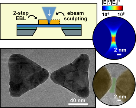
Solid-state plasmonic nanopores are an emerging class of single-molecule biosensors that show great promise for label-free manipulation and interrogation of the biomolecule of interest. The integration of a plasmonic nanoantenna and a nanopore brings new functionalities to the nanopore that arise from the strong light-matter interactions in the antenna. For instance, localized optical heating of the plasmonic nanostructures at the nanopore has been used to precisely control the temperature near the nanopore[1] and to enhance the DNA capture rate[2]. More importantly, the extreme light concentration by the plasmonic nanoantenna has been used to trap nanometer-sized particles inside a nanoslit[3] and simulations have predicted that this optical force can be used for controlling the translocation of a single DNA molecule[4]. Furthermore, the localized electromagnetic field is strongly enhanced at the nanoantenna, which creates routes for optical readout, such as surface-enhanced fluorescence[5] and surface-enhanced Raman spectroscopy[6] that can complement the traditional ionic current readout. Nanopore sensing will benefit from optical readout strategies as detection schemes allow for low noise acquisition at high bandwidth[7] and optical signals can carry rich information about the chemical composition of the analyte[8].
Plasmonic-nanogap-based structures are a superior class of plasmonic nanoantennas as they can generate extremely localized electromagnetic-field (|E|2) enhancements of up to 104 [9] when the gap mode is excited. These intense enhancements greatly boost fluorescence[10], third harmonic generation[11], and Raman scattering probabilities enabling single-molecule detection and characterization[8]. Moreover, by controlling the size of the nanogaps, the confinement of the optical field can be tailored such that only a single molecule can fit the sensing volume. While the gap-based plasmonic structures focus light field into a sub-diffraction-limit hot spot region, the maximum attainable intensity of the electromagnetic field is strongly affected the geometry of the nanostructure[12] and, in particular, its feed-gap size[13]. The dependence of the electromagnetic-field (EM) enhancement on the gap size has been extensively studied[14] and observed to dramatically increase with decreasing gap size. The strongest field enhancements are created in gaps down to ~1 nm in size[14–15], as non-local effects[16] and quantum tunneling[17] limit further enhancement for smaller gap sizes. Hence, for the strongest possible field enhancement it is essential to fabricate gap sizes down to only a few nanometers in size.
The fabrication of such nanometer sized feed-gaps is challenging, especially if they have to be integrated with nanopores. Both bottom-up and top-down approaches to fabricate nanogap-based plasmonic antennas have been demonstrated[18]. Using bottom-up synthesis, small nanogaps have been realized in nanoparticle aggregates[19], and DNA-encoded nanoparticle self-assembly[20]. Whereas these techniques have shown to produce small nanogaps and can be extended to large-scale essays, they are not well suited for nanopore integration. Top-down approaches do allow naturally for nanopore integration and yield well-defined nanostructures with good reproducibility[21]. However, nanoscale top-down patterning techniques like e-beam lithography (EBL) have a limited resolution[22], which makes fabricating nanometer-sized gap structures with reasonable yield very challenging.
To overcome these challenges, we here report a top-down fabrication technique to integrate an ultra-small nanogap (~3 nm) plasmonic antennas with a solid-state nanopore. In short, we fabricated bowtie-antenna plasmonic nanopores (Figure 1a), using a 2-step EBL patterning on a free-standing membrane, where our multistep approach allows to bypass the resolution limit of the conventional EBL. We used focused electron-beam sculpting with a transmission electron microscope (TEM) to subsequently drill a nanopore in the gap of the antenna. The fabricated nanostructures were examined using high-resolution transmission electron microscopy (HRTEM). Finally, we performed DNA translocations to demonstrate that these small nanogap plasmonic nanopores can be used for single molecule sensing.
Figure 1. Schematic of the plasmonic solid-state nanopore and the simulated electromagnetic field intensity.
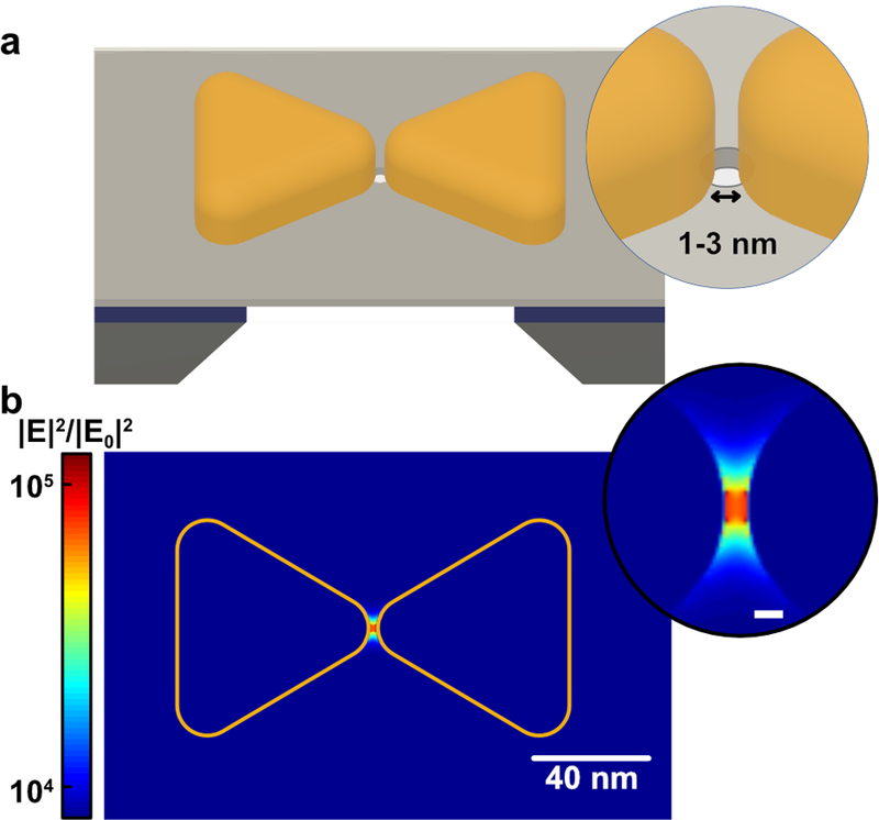
(a) Schematic of a solid-state nanopore with an integrated bowtie antenna structure. The bowtie antennas with ultra-small nanogaps (1–3 nm typically) are fabricated on free-standing SiN membrane, with a nanopore drilled in the center of the gap; (b) FDTD simulation of the near-field electromagnetic (EM) field intensity distribution around a bowtie structure with a 2-nm gap under longitudinal excitation at the resonant wavelength. The inset shows the EM field intensity in the nanogap (scale bar: 2 nm).
To estimate the maximum intensity of the EM field generated by the plasmonic nanogaps, we performed finite-difference time-domain (FDTD) simulations on bowtie antennas with nanopores. Figure 1b shows the simulated electric near-field intensity distribution of a bowtie antenna excited with longitudinal polarized laser at its resonant wavelength (900 nm). The EM hotspot localizes in the gap of the bowtie antenna, where it creates a ~104 EM intensity (|E|2) enhancement. In Supplementary Figure S1, we plot the dependence of the EM enhancement on the wavelength at the center of the gap. When the gap size decreases from 5 nm to 1 nm, the |E|2/|E0|2 increases more than 20 times. The common figure of merit in plasmonics is |E|4, which is the enhancement factor (EF) for surface-enhanced optical sensing. Values for EF are calculated to be larger than 108 for gaps smaller than 5 nm, and can be improved by about 5 order-of-magnitude, up to values >1011, when decreasing the gap size from 5 nm to 1 nm, see Fig.S1. For applications like surface-enhanced Raman spectroscopy, it is crucial to reproducibly obtain hotspots with an EF larger than 108 to achieve the single-molecule sensitivity[13].
Fabrication of ultra-small, especially sub-3 nm sized nanogaps is beyond the resolution of the conventional electron-beam lithography process. This resolution is typically limited by forward- and backscattered electrons that are generated elsewhere in the substrate and resist by the exposing electron beam. These backscattered electrons expose the resist at remote locations and this proximity effect significantly reduces the spatial patterning resolution of the EBL. We would like to note that although the proximity effect can be mitigated substantially by patterning on a thin membrane[23], achieving reliably sub-3-nm gap sizes remains challenging due short-range proximity effects caused by a relatively large electron-beam spot-size in conventional electron-beam pattern generators.
To surpass the conventional EBL resolution limit, we employed a 2-step EBL patterning[24]. A schematic of the full fabrication process is shown in Figure 2. Starting from a substrate with a free-standing SiN membrane, a layer of resist is spin coated on the substrate for the first patterning step. Then an array of one half of the bowtie nanostructures, alongside a set of marker structures, is patterned into the resist with an electron beam and developed. Subsequently, 30 nm of gold is evaporated onto the substrate and lift-off process is performed. Next, in the second step, a new layer is spin coated on the same substrate, and the same process is repeated but now for the second half of the bowtie antennas. The two patterns are aligned by an automated search for the marker structures defined in the first step. Finally, a nanopore is drilled in the gap of the antenna using a TEM. Details of the fabrication process can be found in the experimental section.
Figure 2. Fabrication process of sub-3-nm gaps integrated with solid-state nanopores.
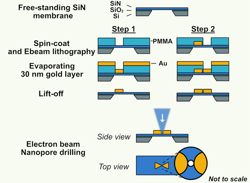
A 2-step electron-beam lithography (EBL) was used to create a bowtie nanoantenna with ultrasmall gap on a free-standing silicon nitride (SiN) membrane supported by a silicon oxide layer and a silicon frame. Subsequently a nanopore is drilled using the focused electron beam of a transmission electron microscope (TEM).
With this approach, the feed-gap size will now not be limited by the EBL resolution, but be set by the accuracy of the automated marker search that is used in the second patterning step to align the first and second patterns. The typical precision of pattern alignment using this routine is about ±10 nm, which by itself does not present an improvement over the single-step EBL resolution. However, this error in alignment can be compensated by deliberately writing an array of slightly mismatched bowtie nanostructures. By writing the second half of the bowtie progressively offset in X and Y within the plane by at the design level (Supplementary Figure S2) extremely small nanogaps will be created somewhere in the array. There are three advantages of using this kind of mismatched array. First, in case the alignment of the second pattern has a small error, a sub-1-nm gap in between the dimers will be achieved, not necessarily at the designed location, but elsewhere in the written pattern. To ensure that at least one sub-1-nm nanogap can be found on the free-standing membrane, we recursively offset patterns in 30 rows and columns each with 1 nm, to allow alignment errors within ±15 nm. Second, since the EBL does not set the resolution of the gap size, the process is compatible with any high resolution EBL resist and substrate. Finally, this method creates bowtie antennas with varying gap sizes ranging from <1 nm up to 10–15 nm. Hence a gap of a suitable size for the intended experiment can be chosen as the preferred site for TEM drilling.
Figure 3a shows a HRTEM image of a typical small-gap bowtie nanostructures fabricated using the described 2-step EBL method. The 30 nm thick gold nanostructure consists of 2 equilateral triangles with a 80-nm width and a tip rounding with a ~10 nm radius, in accordance with the EBL beam spot size. Figure 3b shows a zoom of a 0.5-nm gap of a typical structure, which is 0.5nm. Figure 3c and 3d show TEM images of ~1.5 and ~2.2 nm gaps.
Figure 3. TEM images of bowtie structures with different gap-sizes.
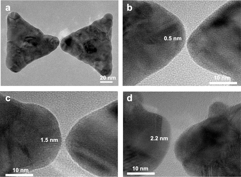
(a) TEM image of a typical bowtie structure with an ultra-small nanogap. (b-d) Close-up TEM images of bowtie structure with 0.5-nm (b), 1.5-nm (c), and 2.2-nm (d) nanogaps.
After nanostructure fabrication, a nanopore was drilled with a TEM in the small feed-gap of the nanoantenna. To precisely fit the small gaps, the beam is focused down to about 1 nm. Figure 4a-b shows examples of nanopores drilled in a bowtie antenna in the same antenna as displayed in Figure 3b and 3c. As is clear from Figure 4a-b, a slight drilling-induced gap expansion can be observed from 0.5 to ~2 nm and from 1.5 nm to ~1.8 nm, respectively. This gap expansion during drilling is typical, as illustrated by the additional examples in the Supplementary Figure S3. The expansion dictates a lower limit of gap sizes that can be achieved for plasmonic nanopores with this technique and restricts the fabrication to nanogaps larger than 1 nm. Gap sizes down to 2 nm gaps for nanoantennas with nanopores can be readily obtained. Sometimes, gap shrinkage rather than gap expansion was observed, which usually results in bridge formation between the bowtie antennas, as shown in Supplementary Figure S4. Such electron-beam induced shrinking is typically more pronounced for a poorly focused electron beam, suggesting that this may result from electron beam induced gold-atom interdiffusion[25]. Carbon contamination can also be observed during the TEM drilling if the samples are not thoroughly cleaned, as shown in Supplementary Figure S5. Interestingly, nanopores can be expanded to sizes larger than the nanogap, as shown in Figure 4a-b. Larger nanopore diameters have a larger open-pore current and significantly higher associated biomolecular capture rates, but decrease the efficiency of delivering the target molecules into the hot spot.
Figure 4. TEM images of bowtie structures after nanopore drilling.
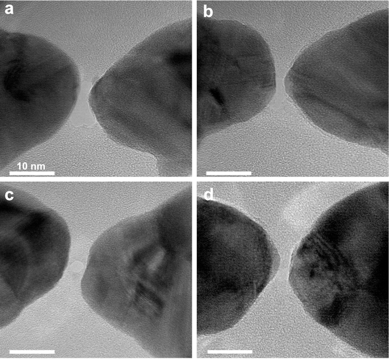
(a-b) shows the same structure as shown in Figure 3b-c. The gap had been expanded into around 2 nm after nanopore drilling. (c-d) Other examples of plasmonic nanopores with an ultra-small nanogap. Scale bars: 10 nm.
Finally, we performed DNA translocation experiments to demonstrate single-molecule detection with a small-gap plasmonic nanopore and characterize the effect of plasmon excitation on the DNA translocation. A schematic of the experiment is shown in Figure 5a. A nanopore chip was placed in a flow cell containing a 2M LiCl electrolyte solution. Next, double-stranded DNA was added to one compartment of the flow cell and electrophoretically driven through the nanopore by an applied bias voltage. The DNA molecule obstructs the nanopore during translocation, leading to a transient blockade of the ionic current that was set up by the bias voltage. The small-gap plasmonic nanostructure was excited in the longitudinal mode using 785 nm wavelength laser light in a confocal configuration. Experimental details are described in the experimental section.
Figure 5. Typical current traces from DNA translocations through plasmonic nanopores with ultra-small nanogaps.
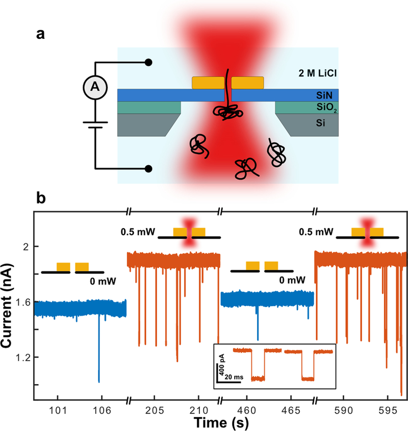
(a) Schematic of the experimental setup for plasmonic nanopore DNA translocation experiments. (b) Typical current traces during a DNA translocation experiment under 100 mV bias voltage without (blue) and with (orange) laser excitation, with 2 zooms of sample translocation events during laser excitation at higher time resolution. 48.5bp λ-DNA was used in the experiment. The current trace is low-pass filtered at 10kHz. A corresponding scatter plot is shown in Supplementary Figure S6.
Figure 5b shows typical current traces with and without laser excitation of the plasmonic nanostructure (TEM image shown in Supplementary Figure S6) at 100 mV, using a plasmonic nanopore with a open pore conductance of 15 nS. This is equivalent to a nanopore with an effective diameter of ~4 nm, using an effective membrane thickness of 7 nm[26]. First, we notice a strong current increase from 1.55 to 1.90 nA upon laser excitation of the plasmonic nanopore with 0.5 mW of laser power. This current increase can be attributed to plasmonic heating of the nanopore and corresponds to a temperature increase of about 15 ℃[1b]. Second, a marked increase in the event rate of the DNA molecules can be observed. Whereas in absence of laser excitation, very few translocations are observed, many more can be discerned during plasmon excitation. This enhancement of the event rate is consistent with previously observed DNA translocations in LiCl through larger-size plasmonic nanopores, and can be attributed to thermophilic migration of the DNA molecules towards the locally heated plasmonic antenna[2]. Finally, we notice that the DNA translocations during plasmon excitation are almost exclusively single file (unfolded), as dictated by the small 4 nm pore, with a large spread in the DNA translocation times (Supplementary Figure S6). These long translocation times may be an effect of plasmon excitation, but at this point we cannot rule out that they result from interactions of DNA with the pore. [27]. Summing up, we conclude that the observation of single well-defined DNA translocations demonstrate the feasibility of using small-gap plasmonic nanopores as single molecule DNA sensors.
In conclusion, we have developed a method to integrate sub-3-nm plasmonic gaps with solid-state nanopores. By using 2-step EBL patterning, the limit of EBL resolution could be surpassed to routinely obtain plasmonic nanostructures with even sub-1-nm feed-gaps. Next, nanopores were successfully manufactured in the small nanogaps using TEM drilling. Electron beam irradiation during drilling expanded the smallest gaps slightly, which sets the lower limit of the nanogaps sizes for plasmonic nanopores to 1 nm. Since nanometer-sized feed gaps are critical to generate extremely intense plasmonic fields, we believe that this method constitutes an important step towards realizing plasmonic nanopores that make optimal use of the advantages that plasmonic hotspots have to offer, such as surface enhanced Raman spectroscopy. Finally, this fabrication process to create nanopores in ultra-small gaps will also be of merit to alternative transverse detection schemes, such as tunneling current detection, which can characterize single-molecules traversing the nanopore.
Experimental Section
Fabrication details
First, the free-standing SiN membranes are fabricated as explained in [28]. In brief, SiN/SiO2 coated silicon wafers were patterned on the backside using photolithography. Then reactive ion etching (RIE) was used to remove the protective SiN/SiO2 layers to expose the silicon for subsequent KOH wet etching. After KOH wet etching to remove the silicon and free up SiN/SiO2 membrane, another RIE step was used to remove the protective layer SiN layer at the front side and a buffered oxide etch (BOE) was used to create a 20 nm thick free-standing SiN membrane, with typical sizes ranging from 30 μm×30 μm to 60 μm×60 μm. Next, an array of plasmonic bowtie nanoantennas, consisting of two equilateral triangles with a tip-to-base height of 80 nm, is defined using EBL in two consecutive steps. For each EBL step, we first spin-coated ~100 nm PMMA resist layer (950K MW , 3% in anisole) on the SiN membranes. In the first step, an array of the left-hand triangles of the bowtie nanostructures and alignment marks for the second step are written using a Raith EBPG 5200 electron beam lithography system, at accelerating voltage of 100 kV, with pressure below 5×10⁻⁷ mBar. The resists were exposed with e-beam doses ranging from 2000–2500 μC/cm2. In the second step, the complementary right-hand triangles are written. The first-step patterns were manually aligned to the center of the free-standing membranes, while the second-step patterns were aligned by an automatic mark search routine on the markers fabricated in the first EBL step. All the patterns were developed in a mixture of methyl isobutyl ketone (MIBK) and isopropanol (IPA) with a volume ratio of 1:3 (MIBK:IPA) for 60 s. Electron Beam Evaporation was then performed to deposit a 30-nm gold layer with 1-nm Titanium as adhesion layer at a pressure below 2.0×10⁻⁶ Torr. The resist was subsequently removed using lift-off by immersing the device overnight in 80 ℃ PRS-3000 solution. Finally, a single nanopore was drilled using a TEM (FEI Tecnai 200S) on each free-standing membrane. The electrons were accelerated under a tension of 200 kV and focused on the SiN membranes, with a beam current density of 108-109 e/nm2/s.
DNA translocation experiment
After oxygen plasma treatment a plasmonic nanopore chip is placed in a flow cell containing 2M LiCl electrolyte solution. Next, Double-stranded DNA (48.5 kbp, 10 ng/μL) is added to the compartment of flow cell facing the etch pit of the chip and electrophoretically driven through the nanopore by an applied bias voltage. The voltage is applied by a pair of Ag/AgCl electrodes connected to a patch clamp amplifier (Axon Axopatch 200B, Molecular Devices). The DNA molecule obstructs the nanopore during translocation, leading to a transient blockade of the ionic current that is set up by the bias voltage. The small-gap plasmonic nanostructure is excited using a 785 nm laser, polarized longitudinally along the line that connects the dimers of the antenna. The plasmonic nanopore is located on the chip by monitoring nanopore ionic current while scanning the membrane with a laser beam. The excitation of the plasmonic structure in the vicinity of the nanopore will result in ionic current increase due to local heating of the electrolyte near the nanopore. Further experimental details are described elsewhere[2]
Supplementary Material
Acknowledgments
This work was supported by National Human Genome Research Institute of the National Institute of Health under Award Number 1R01HG007406–01 and the European Research Council Advanced Grant SynDiv (No. 669598). We would like to thank Meng-Yue Wu for drilling nanopores. Xin Shi is sponsored by the China Scholarship Council (201606740021).
Footnotes
Supporting Information
Supporting Information is available from the Wiley Online Library.
References
- [1].(a) Crick CR, Albella P, Ng B, Ivanov AP, Roschuk T, Cecchini MP, Bresme F, Maier SA, Edel JB, Nano letters 2014, 15, 553–559; [DOI] [PubMed] [Google Scholar]; (b) Jonsson MP, Dekker C, Nano letters 2013, 13, 1029–1033. [DOI] [PubMed] [Google Scholar]
- [2].Nicoli F, Verschueren D, Klein M, Dekker C, Jonsson MP, Nano letters 2014, 14, 6917–6925. [DOI] [PMC free article] [PubMed] [Google Scholar]
- [3].Chen C, Juan ML, Li Y, Maes G, Borghs G, Van Dorpe P, Quidant R, Nano letters 2011, 12, 125–132. [DOI] [PubMed] [Google Scholar]
- [4].Belkin M, Chao S-H, Jonsson MP, Dekker C, Aksimentiev A, ACS nano 2015, 9, 10598–10611. [DOI] [PMC free article] [PubMed] [Google Scholar]
- [5].(a) Assad ON, Gilboa T, Spitzberg J, Juhasz M, Weinhold E, Meller A, Advanced Materials 2017, 29, 1605442; [DOI] [PubMed] [Google Scholar]; (b) Nam S, Choi I, Fu C.-c., Kim K, Hong S, Choi Y, Zettl A, Lee LP, Nano letters 2014, 14, 5584–5589. [DOI] [PubMed] [Google Scholar]
- [6].Cecchini MP, Wiener A, Turek VA, Chon H, Lee S, Ivanov AP, McComb DW, Choo J, Albrecht T, Maier SA, Nano letters 2013, 13, 4602–4609. [DOI] [PubMed] [Google Scholar]
- [7].Gilboa T, Meller A, Analyst 2015, 140, 4733–4747. [DOI] [PubMed] [Google Scholar]
- [8].Zrimsek AB, Chiang N, Mattei M, Zaleski S, McAnally MO, Chapman CT, Henry A-I, Schatz GC, Van Duyne RP, Chemical Reviews 2017, 117, 7583–7613. [DOI] [PubMed] [Google Scholar]
- [9].Xu H, Aizpurua J, Käll M, Apell P, Physical Review E 2000, 62, 4318. [DOI] [PubMed] [Google Scholar]
- [10].Kinkhabwala A, Yu Z, Fan S, Avlasevich Y, Müllen K, Moerner W, Nature Photonics 2009, 3, 654–657. [Google Scholar]
- [11].Aouani H, Rahmani M, Navarro-Cía M, Maier SA, Nature nanotechnology 2014, 9, 290–294. [DOI] [PubMed] [Google Scholar]
- [12].McFarland AD, Young MA, Dieringer JA, Van Duyne RP, The Journal of Physical Chemistry B 2005, 109, 11279–11285. [DOI] [PubMed] [Google Scholar]
- [13].Nam J-M, Oh J-W, Lee H, Suh YD, Accounts of chemical research 2016, 49, 2746–2755. [DOI] [PubMed] [Google Scholar]
- [14].Zhu W, Esteban R, Borisov AG, Baumberg JJ, Nordlander P, Lezec HJ, Aizpurua J, Crozier KB, Nature communications 2016, 7, 11495. [DOI] [PMC free article] [PubMed] [Google Scholar]
- [15].Marinica DC, Kazansky AK, Nordlander P, Aizpurua J, Borisov A, Nano letters 2012, 12, 1333–1339. [DOI] [PubMed] [Google Scholar]
- [16].Ciracì C, Hill R, Mock J, Urzhumov Y, Fernández-Domínguez A, Maier S, Pendry J, Chilkoti A, Smith D, Science 2012, 337, 1072–1074. [DOI] [PMC free article] [PubMed] [Google Scholar]
- [17].(a) Zhu W, Crozier KB, Nature communications 2014, 5, 5228; [DOI] [PubMed] [Google Scholar]; (b) Scholl JA, García-Etxarri A, Koh AL, Dionne JA, Nano letters 2013, 13, 564–569. [DOI] [PubMed] [Google Scholar]
- [18].Ding S-Y, Yi J, Li J-F, Ren B, Wu D-Y, Panneerselvam R, Tian Z-Q, Nature Reviews Materials 2016, 1, 16021. [Google Scholar]
- [19].Kneipp K, Kneipp H, applied spectroscopy 2006, 60, 322A–334A. [DOI] [PubMed] [Google Scholar]
- [20].(a) Lim D-K, Jeon K-S, Kim HM, Nam J-M, Suh YD, Nature materials 2010, 9, 60; [DOI] [PubMed] [Google Scholar]; (b) Thacker VV, Herrmann LO, Sigle DO, Zhang T, Liedl T, Baumberg JJ, Keyser UF, Nature communications 2014, 5, 3448. [DOI] [PubMed] [Google Scholar]
- [21].Banholzer MJ, Millstone JE, Qin L, Mirkin CA, Chemical Society Reviews 2008, 37, 885–897. [DOI] [PMC free article] [PubMed] [Google Scholar]
- [22].Manfrinato VR, Zhang L, Su D, Duan H, Hobbs RG, Stach EA, Berggren KK, Nano letters 2013, 13, 1555–1558. [DOI] [PubMed] [Google Scholar]
- [23].Fischbein MD, Drndić M, Applied physics letters 2006, 88, 063116. [Google Scholar]
- [24].Wang D, Zhu W, Best MD, Camden JP, Crozier KB, Nano letters 2013, 13, 2194–2198. [DOI] [PubMed] [Google Scholar]
- [25].Liu Y, Sun Y, Nanoscale 2015, 7, 13687–13693. [DOI] [PubMed] [Google Scholar]
- [26].Kowalczyk SW, Grosberg AY, Rabin Y, Dekker C, Nanotechnology 2011, 22, 315101. [DOI] [PubMed] [Google Scholar]
- [27].Wanunu M, Sutin J, McNally B, Chow A, Meller A, Biophysical Journal 2008, 95, 4716–4725. [DOI] [PMC free article] [PubMed] [Google Scholar]
- [28].Janssen XJ, Jonsson MP, Plesa C, Soni GV, Dekker C, Dekker NH, Nanotechnology 2012, 23, 475302. [DOI] [PubMed] [Google Scholar]
Associated Data
This section collects any data citations, data availability statements, or supplementary materials included in this article.


