

Summary
Commercially available electrochromic (EC) windows are based on solid-state devices in which WO3 and NiOx films commonly serve as the EC and counter electrode layers, respectively. These metal oxide layers are typically physically deposited under vacuum, a time- and capital-intensive process when using rigid substrates. Herein we report a facile solution deposition method for producing amorphous WO3 and NiOx layers that prove to be effective materials for a solid-state EC device. The full device containing these solution-processed layers demonstrates performance metrics that meet or exceed the benchmark set by devices containing physically deposited layers of the same compositions. The superior EC performance measured for our devices is attributed to the amorphous nature of the NiOx produced by the solution-based photodeposition method, which yields a more effective ion storage counter electrode relative to the crystalline NiOx layers that are more widely used. This versatile method yields a distinctive approach for constructing EC windows.
Subject Areas: materials science, coatings, energy materials
Graphical Abstract
Highlights
-
•
Amorphous WO3 and NiOx films are produced by a solution-deposition method
-
•
The WO3 and NiOx films are assembled into a solid-state electrochromic device
-
•
The solid-state device exhibits state-of-the-art electrochromic performance
-
•
Amorphous NiOx is a superior counter electrode material compared with crystalline NiOx
Materials Science; Coatings; Energy Materials
Introduction
Electrochromic (EC) windows (also known as smart or dynamic windows) undergo changes in light transmittance in response to an applied voltage, enabling the dynamic control of daylight and solar heat passing through buildings (Granqvist, 2006, Granqvist, 2012a, Runnerstrom et al., 2014). This technology can provide both indoor thermal and visual comfort for building occupants while improving building energy efficiency by as much as 20% (Granqvist, 2012a). These features have prompted substantial investment into deploying EC windows at scale, but the high price of such windows ($1,000/m2 c.f. ∼$150/m2 for a regular window (Smart windows cost, 2016)) has prevented their widespread use. A significant fraction of the cost is imbedded in the vacuum environment required to sputter EC window layers. This process can require a substantial capital outlay, and the long residence times needed to fabricate the key layers on rigid substrates also preclude rapid throughput (Garg et al., 2005). These factors present the impetus to develop solution-based deposition methodologies to reduce the costs associated with fabricating EC windows (Barile et al., 2017, Cai et al., 2016a, Llordés et al., 2016).
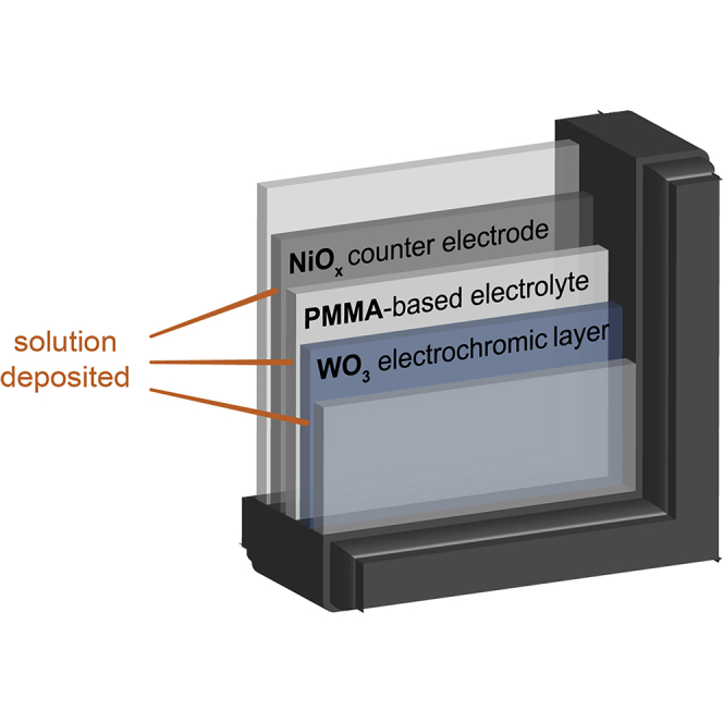
A conventional EC window consists of an EC layer, an electrolyte layer, and an ion storage counter electrode sandwiched between two transparent conducting layers (Figure 1). Thin films of WO3 and NiOx are widely used as the respective EC and counter electrode layers in commercial EC windows (Gillaspie et al., 2010, Niklasson and Granqvist, 2006). Both of these layers contribute to reversible color switching in response to an electrical bias (Figure 1). The NiOx layers are lithiated to form LiyNiOx before device assembly to provide a source of intercalating Li+ during reduction (coloration) of WO3. A voltage applied to the assembled device drives coloration of both metal oxide layers as Li+ migrates into the WO3 layer. The ion-conducting and electrically insulating electrolyte layer serves to shuttle Li+ between the metal oxide layers and prevent short circuiting of the device. Liquid electrolytes are common in academic studies, but solid polymer-based electrolytes are used in commercial systems to satisfy safety and sealing issues (Granqvist, 2012b, Thakur et al., 2012).
Figure 1.

Working Principles for an Electrochromic Device
Scheme outlining the coloration and bleaching process of an EC device with a WO3 electrochromic layer and NiOx counter electrode layer sandwiched between two transparent conductive glass substrates. The pristine device is formed by transparent LiyNOx and WO3 layers and an interstitial electrolyte. Applying a forward bias to the electrochromic layer of the device injects electrons into WO3, which are then compensated by Li+ migrating from the counter electrode through the electrolyte to yield colored LixWO3. The simultaneous extrusion of Li+ from LiyNiOx enables the formation of colored Liy-zNOx. The bleaching process is obtained by applying a reverse bias, yielding the initial LiyNiOx and WO3 transparent layers. The coloration and bleaching processes are summarized by the overall reversible reaction shown in the Scheme.
The EC behavior of these layers is exquisitely sensitive to impurities, film defects, thickness, porosity, and crystallinity (Cai et al., 2016b, Granqvist, 2014, Lee et al., 2006, Scherer and Steiner, 2013). These factors therefore impose very stringent conditions on how EC windows can be manufactured. Physical vacuum deposition has emerged as the most reliable and scalable method of producing uniform and optical-quality metal oxide films of variable thicknesses (Thummavichai et al., 2017). Notwithstanding, the metal oxide semiconductor industry teaches that manufacturing methods progressively transition from vacuum to solution-processing methods to reduce costs (Yu et al., 2016). The ability to solution process at ambient temperatures and pressures offers the opportunity to reduce energy consumption and capital equipment while also reducing processing times (Llordés et al., 2016). Moreover, the avoidance of high vacuum lessens the safety concerns associated with handling potentially hazardous materials (e.g., lithium-containing chemicals). There are several reports of solution-based methods for processing EC or counter electrode layers, including electrodeposition (Baeck et al., 2003, Cai et al., 2016b), chemical bath deposition (Ristova et al., 2002, Vidales-Hurtado and Mendoza-Galván, 2008, Xia et al., 2008), sol-gel methods (Livage and Ganguli, 2001), and spray pyrolysis (Kamal et al., 2005, Tenent et al., 2010). However, none of these methods are well suited for synthesizing both WO3 and NiOx films. Consequently, these layers are evaluated in electrochemical half-cells or in devices in which the working or counter electrode is physically deposited (Jiao et al., 2003, Srivastava et al., 2005, Zhang et al., 2009). These observations motivated us to build an EC device wherein all layers are solution-processed.
We demonstrate herein the use of a “photodeposition” method (Cheng et al., 2018, Smith et al., 2013) to solution-process both the WO3 and NiOx EC layers of an EC device with a solution-deposited poly(methyl methacrylate) (PMMA)-based electrolyte. To our knowledge, this is the first report of a solid-state EC device containing internal layers that are fully solution-processable at low temperature. The performance of our laboratory-scale solid-state EC devices meets or exceeds current literature benchmarks in terms of optical modulation (ΔT633 nm; measured as the difference in light transmittance between the fully colored and bleached states at λ = 633 nm), switching time for coloration (tcolor; defined by the time required to reach 90% of a transmittance change from the fully bleached to fully colored state) and bleaching (tbleach), and coloration efficiency (CE; the change in optical density acquired by injection of charge per unit area; Table 1). We also demonstrate the superior performance of amorphous thin film materials in EC windows by directly comparing amorphous and crystalline NiOx counter electrodes in the same device architecture and produced by analogous solution-based methods. This study presents an opportunity to harness low-cost solution-processing methods for the production of high quality EC devices.
Table 1.
Performance Parameters of Our Solid-State EC Devices in Comparison with That of Solid-State Devices Reported in the Literature
| Counter Electrode Material | Phase | Deposition Method | ΔT (%) | tcolor (s) | tbleach (s) | CE (cm2/C) | Reference |
|---|---|---|---|---|---|---|---|
| NiO porous film | Crystalline | Chemical bath deposition | 55 | 10 | 20 | 87.2 | Zhang et al., 2009a |
| NiO nanoparticle film | Crystalline | Inkjet printing | 75 | 10 | 13 | 131.9 | Cai et al., 2016ab |
| NiOx film | Crystalline | Magnetron sputtering | 52 | 5 | 2 | – | Liu et al., 2016c |
| NiOxfilm | Amorphous | Photodeposition | 60 | 4 | 6 | 141 | this workd |
| NiOxfilm | Crystalline | Photodeposition | 26 | 78 | 17 | 72 | this workd |
All devices use WO3 as the electrochromic layer, NiOx as the counter electrode, and a polymer-based electrolyte.
Measured at 633 nm over the −2.5 to +2.5 V potential range.
Measured at 550 nm over the −2.5 to +2.5 V potential range.
Measured at 550 nm over the −1.8 to +1.8 V potential range.
Measured at 633 nm over the −2.1 to +2.1 V potential range.
Results and Discussion
Electrode Synthesis and Device Assembly
Amorphous tungsten oxide (a-WO3) films were prepared using a photodeposition methodology known to yield amorphous metal oxide layers (Cheng et al., 2018, He et al., 2017, Smith et al., 2013). Briefly, a solution of WCl6 in 2-propanol was spin-cast onto a fluorine-doped tin oxide (FTO) substrate and the resultant precursor film was irradiated with UV light (λmax = 185 nm) to form a metal oxide film. Characterization of the films by top-view and cross-sectional scanning electron microscopy (SEM) was consistent with the successful formation of porous a-WO3 films of ∼600 nm thickness (Figure S1). NiOx films were prepared following a similar procedure: aqueous solutions of 0.25 M NiCl2 were spin-cast onto an FTO substrate followed by UV irradiation (λmax = 185 nm) for 8 hr. The complete liberation of chlorine from the precursor film and the formation of NiOx was confirmed by X-ray fluorescence and X-ray photoelectron spectroscopy analyses (Figure S2). The X-ray diffraction (XRD) pattern of the as-prepared NiOx films showed a broad reflection centered at 2θ = 18° indexed to the (001) facets of α-Ni(OH)2 (Smith et al., 2016), together with the reflections corresponding to the FTO substrate (Figure S3). This broad reflection was no longer observed, and no additional reflections appeared after annealing the NiOx films at 200°C for 1 hr, which denotes the successful formation of amorphous films (Figure S3). The thickness of a-NiOx films prepared by spin casting and UV treating five layers of NiCl2 precursor on the FTO substrate before the annealing step was determined to be 120 nm by cross-sectional SEM (Figure 2). Cross-sectional and top-view SEM images (Figures 2 and S4A) show that the NiOx films follow the contour of FTO and have smooth uniform surfaces. Crystalline NiOx (c-NiOx) films were also obtained by annealing the as-deposited NiOx films at 400°C for 1 hr. The resulting XRD pattern shows well-defined reflections corresponding to crystalline cubic NiO (Figure S3). Five-layer c-NiOx films show smooth uniform surfaces with a thickness of 105 nm (Figures S4B and S4C).
Figure 2.

SEM Characterization of Amorphous NiOx Films
Cross-sectional SEM images of five-layer a-NiOx films produced by photodeposition followed by annealing at 200°C for 1 hr. Cross-sectional SEM images were acquired on fresh edges of cleaved samples at a tilt angle of 52°. See also Figures S1–S4, S6, and S7.
Solid-state EC devices with active areas of ∼2 cm2 were assembled using a-WO3 films coated on FTO glass as the working electrode, either a- or c-NiOx films deposited on FTO glass as the counter electrode, and a PMMA-based gel as the electrolyte. NiOx counter electrodes were lithiated before device assembly by submerging the films in 1 M LiClO4 propylene carbonate and applying a potential of −1.5 V (vs Ag/AgCl) across the cell for 5 min. The PMMA-based gel electrolyte was drop-cast directly onto the a-NiOx electrode and contained within a silicone spacer with a thickness of 1 mm. The device was completed with the a-WO3 working electrode and sealed with epoxy glue.
Electrochromic Performance of Solid-State Devices
The EC performance of the full devices containing either a- or c-NiOx counter electrode was tested by using UV-Vis spectroscopy to measure the optical properties under applied potentials (Figure 3). The optical modulation (ΔT633 nm) was determined by recording the transmittance of the devices in either a fully colored or a fully bleached state at potentials of −2.1 or +2.1 V, respectively. EC devices with the a-NiOx counter electrode showed a ΔT633 nm–60%, compared with ΔT633 nm–26% for the device with c-NiOx counter electrode (Figure 3A) (c.f. 19% for devices in which the counter electrode was bare FTO [Figure S5]). Switching times from the fully colored to the fully bleached state (tbleach), and the reverse (tcolor), were measured by tracking the transmittance at λ = 633 nm in response to consecutive applied potentials of +2.1 and −2.1 V for 30 s each (Figure 3B). The device with the a-NiOx counter electrode showed rapid switching times of tbleach ∼ 6 s and tcolor ∼4 s, whereas the device with a c-NiOx counter electrode showed much slower tcolor and tbleach of 78 and 17 s, respectively.
Figure 3.

Amorphous NiOx Layers Make Superior Counter Electrodes
(A) Transmittance spectra of EC devices using a-NiOx (orange trace) and c-NiOx (black trace) as counter electrodes at colored and bleached states. The spectra were recorded after coloring at −2.1 V or bleaching at +2.1 V for 60 s. The images are the solid-state device using a-NiOx as counter electrode in bleached and colored states.
(B) Transmittance change at wavelength of 633 nm for the EC devices with a-NiOx (orange trace) and c-NiOx (black trace) on FTO as counter electrode as a function of time. The devices were bleached at +2.1 V for 30 s, then colored at −2.1 V for another 30 s. Switching times tcolor and tbleach are indicated.
(C) Changes in optical density of the devices using a-NiOx and c-NiOx (inset) on FTO as counter electrode at 633 nm as a function of charge density. Coloration efficiency values were determined by fitting the linear region of the plot (Equation 1 and 2).
See also Figures S5, S8, and S9.
CE, which measures the change in optical density acquired by injection of charge per unit area, was determined in accordance with Equations 1 and 2:
| (Equation 1) |
| (Equation 2) |
where Δ(OD) is the change in optical density and ΔQ is the charge density (C/cm2) obtained from electrochemical measurements; Tb is the maximum transmittance in the bleached state at a fixed wavelength (obtained from Figure 3B); and Tc is the varying transmittance obtained during the coloration process at this same wavelength. The CE values derived from the slope of the linear region of Δ(OD) versus ΔQ (Figure 3C) were determined to be 141 cm2/C for a device containing an a-NiOx counter electrode. This value is approximately twice that of the device with c-NiOx counter electrode (72 cm2/C).
The differences in performance metrics of the EC devices containing either an a-NiOx or c-NiOx counter electrode demonstrate the superior EC performance of a-NiOx systems. It appears that the superior performance of a-NiOx is manifest in the superior ion-storage properties of the films given that a-NiOx is characterized by a charge capacity of 4.1 mC/cm2 during the pre-lithiation process that is 2-fold higher than the value measured for c-NiOx (1.6 mC/cm2). These findings are consistent with the higher ion storage capacity generally observed for amorphous materials (Ku et al., 2012, Lee et al., 2014). The improved ion storage performance that arises in amorphous materials is believed to be due to the larger interstitial spaces between more disordered atoms (Lee et al., 2014, Legrain et al., 2015, Llordés et al., 2016). These larger interatomic spaces can accommodate intercalated ions and facilitate the mobility of ions in materials. In the case of NiOx counter electrode materials in EC devices, the amorphous film is capable of balancing more charges during each EC cycle, thereby accommodating greater lithium insertion into the WO3 during each coloration cycle and resulting in higher ΔT. Furthermore, the enhanced ion mobility in a-NiOx yields faster switching times between bleach and colored states.
Table 1 lists the performance of our solid-state EC devices containing photodeposited NiOx counter electrodes along with other reported devices of similar sizes and configurations. The ΔT633 nm of 60% reported here for the a-NiOx is in keeping with systems synthesized by other methods. The switching times (tbleach and tcolor) of our device is among the fastest reported to date, exceeded only by tbleach for films made using high-vacuum sputtering methods. The CE of 141 cm2/C exceeds all other known examples of devices based on WO3 and NiOx materials, highlighting the excellent EC performance of our solution-processed devices containing amorphous films. It is worth noting that the performance is also comparable with commercially available EC windows, which use sputtered WO3 and NiOx films and polymer-based electrolytes. These full-scale windows typically show an optical modulation of merely ∼45% over the visible light region and a switching time of 15–20 min (with the important caveat that the device sizes are different) (Range of products, 2018).
Performance Dependence on a-NiOx Thickness
The thicknesses of the a-NiOx films are controlled simply by spin casting and UV treating a variable number of NiCl2 precursor layers on the FTO substrate before annealing. NiOx films with thicknesses of 70, 120, 240, and 360 nm were prepared by 3, 5, 10, or 15 layers of deposition, respectively (Figures 2, S6, and S7). Amorphous NiOx films of increasing thicknesses (120, 240, and 360 nm) were assembled into EC devices as the counter electrode material (with all other parameters held constant) and similarly assessed for their optical properties in response to an applied voltage. Increasing thickness of a-NiOx from 120 nm to 360 nm caused a slight decrease in ΔT633 nm from 60% to 56% (Figure S8). Switching times tbleach and tcolor also increased slightly reaching 11 and 13 s, respectively, for the thickest of the three a-NiOx films (Figure S8). The stability of the EC devices was also tested by tracking the transmittance change over time while continuously switching between the colored and bleached states. The thicker NiOx films exhibit enhanced cycling stability despite the loss in optical modulation and increase in switching times. SEM characterization showed that the 120-nm a-NiOx film was compromised during cycling, whereas the morphologies of the thicker films (240 and 360 nm) were mostly maintained (Figure S9). For the device with a 120-nm thickness of a-NiOx, 81% of the initial optical modulation value remained after 100 cycles (Figure 4A). The EC device with a 240-nm thickness of a-NiOx retained 90% of the initial ΔT after 100 cycles and 75% after 200 cycles (Figure 4B). Further increasing the thickness of the a-NiOx film to 360 nm enabled the device to retain nearly 100% of the initial ΔT after 400 cycles (Figure 4C). By contrast, solid-state devices using inkjet-printed WO3 and NiO nanoparticle electrodes retain only 80% ΔT633 nm after 100 cycles, with significant further degradation thereafter (Cai et al., 2016a).
Figure 4.

Thickness-Dependent Electrochromic Cycling Stability
(A–C) Transmittance changes at wavelength of 633 nm as a function of time during the electrochromic switching between colored and bleached states for EC devices using a-NiOx films with thicknesses of (A) 120 nm, (B) 240 nm, and (C) 360 nm as counter electrodes. In each electrochromic cycle, the devices were held at potential −2.1 V for 30 s then switched to +2.1 V for another 30 s.
See also Figure S8.
Conclusion
Solution-based photodeposition of readily available metal precursors (WCl6 and NiCl2) can be used to synthesize both the working and counter electrode materials of EC windows. The exceptional performance of EC devices containing these materials is demonstrated here with amorphous WO3 and NiOx thin films assembled together with a PMMA-based gel electrolyte. The resulting solid-state systems exhibit optical modulations (ΔT633 nm), switching times (tcolor and tbleach), coloration efficiencies (CE), and cycling stabilities commensurate with the best reported devices to date, including those produced by expensive or specialized methods. We also show that this low-temperature process yields amorphous layers of NiOx that act as superior counter electrodes relative to crystalline NiOx, which we anticipate will trigger greater research efforts on the use of amorphous materials for EC devices. These collective results represent an opportunity to drive down the costs of energy-saving EC windows that have already attracted substantial commercial investment.
Limitations of the Study
This study demonstrates the ability to use photodeposition to make uniform EC nickel and tungsten oxide layers. The formation of the photodeposited a-NiOx films must be optimized to compete with sputtering at an industrial scale. Future investigations will also seek to resolve the factors that lead to the increases in transmittance of the bleached state during cycling (Figure 4C).
Methods
All methods can be found in the accompanying Transparent Methods supplemental file.
Acknowledgments
The authors are grateful to the Canadian Natural Science and Engineering Research Council (RGPIN 337345-13), Canadian Foundation for Innovation (229288), Canadian Institute for Advanced Research (BSE-BERL-162173), Canada Research Chairs, and Stewart Blusson Quantum Matter Institute for financial support. Additional thanks to the Center for High-Throughput Phenogenomics for access to SEM facilities. D.M.W. and C.P.B. also wish to acknowledge the generous and ongoing support of Peter Bradshaw.
Author Contributions
C.P.B. supervised the project. W.C. designed and performed the experiments. M.M. carried out XRD measurements. D.J.D. conducted SEM analyses. K.H., C.K., and B.T. assisted with thin film preparation. W.C., D.M.W., and C.P.B. wrote the manuscript with input from all authors.
Declaration of Interests
The authors declare no competing interests.
Published: December 21, 2018
Footnotes
Supplemental Information includes Transparent Methods and 9 figures and can be found with this article online at https://doi.org/10.1016/j.isci.2018.11.014.
Supplemental Information
References
- Baeck S.-H., Choi K.-S., Jaramillo T.F., Stucky G.D., McFarland E.W. Enhancement of photocatalytic and electrochromic properties of electrochemically fabricated mesoporous WO3 thin films. Adv. Mater. 2003;15:1269–1273. [Google Scholar]
- Barile C.J., Slotcavage D.J., Hou J., Strand M.T., Hernandez T.S., McGehee M.D. Dynamic windows with neutral color, high contrast, and excellent durability using reversible metal electrodeposition. Joule. 2017;1:133–145. [Google Scholar]
- Cai G., Darmawan P., Cui M., Chen J., Wang X., Eh A.L.-S., Magdassi S., Lee P.S. Inkjet-printed all solid-state electrochromic devices based on NiO/WO3 nanoparticle complementary electrodes. Nanoscale. 2016;8:348–357. doi: 10.1039/c5nr06995e. [DOI] [PubMed] [Google Scholar]
- Cai G., Cui M., Kumar V., Darmawan P., Wang J., Wang X., Lee-Sie Eh A., Qian K., Lee P.S. Ultra-large optical modulation of electrochromic porous WO3 film and the local monitoring of redox activity. Chem. Sci. 2016;7:1373–1382. doi: 10.1039/c5sc03727a. [DOI] [PMC free article] [PubMed] [Google Scholar]
- Cheng W., He J., Dettelbach K.E., Johnson N.J.J., Sherbo R.S., Berlinguette C.P. Photodeposited amorphous oxide films for electrochromic windows. Chem. 2018;4:821–832. [Google Scholar]
- Garg D., Henderson P.B., Hollingsworth R.E., Jensen D.G. An economic analysis of the deposition of electrochromic WO3 via sputtering or plasma enhanced chemical vapor deposition. Mater. Sci. Eng. B. 2005;119:224–231. [Google Scholar]
- Gillaspie D.T., Tenent R.C., Dillon A.C. Metal-oxide films for electrochromic applications: present technology and future directions. J. Mater. Chem. 2010;20:9585–9592. [Google Scholar]
- Granqvist C.-G. Electrochromic materials: out of a niche. Nat. Mater. 2006;5:89–90. doi: 10.1038/nmat1577. [DOI] [PubMed] [Google Scholar]
- Granqvist C.G. Oxide electrochromics: an introduction to devices and materials. Sol. Energy Mater. Sol. Cells. 2012;99:1–13. [Google Scholar]
- Granqvist, C.G. (2012b). Electrochromic device. World patent WO2012138281A1.
- Granqvist C.G. Electrochromics for smart windows: oxide-based thin films and devices. Thin Solid Films. 2014;564:1–38. [Google Scholar]
- He J., Weekes D.M., Cheng W., Dettelbach K.E., Huang A., Li T., Berlinguette C.P. Photodecomposition of metal nitrate and chloride compounds yields amorphous metal oxide films. J. Am. Chem. Soc. 2017;139:18174–18177. doi: 10.1021/jacs.7b11064. [DOI] [PubMed] [Google Scholar]
- Jiao Z., Wu M., Qin Z., Xu H. The electrochromic characteristics of sol–gel-prepared NiO thin film. Nanotechnology. 2003;14:458. [Google Scholar]
- Kamal H., Elmaghraby E.K., Ali S.A., Abdel-Hady K. The electrochromic behavior of nickel oxide films sprayed at different preparative conditions. Thin Solid Films. 2005;483:330–339. [Google Scholar]
- Ku J.H., Ryu J.H., Kim S.H., Han O.H., Oh S.M. Reversible lithium storage with high mobility at structural defects in amorphous molybdenum dioxide electrode. Adv. Funct. Mater. 2012;22:3658–3664. [Google Scholar]
- Lee S.-H., Deshpande R., Parilla P.A., Jones K.M., To B., Mahan A.H., Dillon A.C. Crystalline WO3 nanoparticles for highly improved electrochromic applications. Adv. Mater. 2006;18:763–766. [Google Scholar]
- Lee J., Urban A., Li X., Su D., Hautier G., Ceder G. Unlocking the potential of cation-disordered oxides for rechargeable lithium batteries. Science. 2014;343:519–522. doi: 10.1126/science.1246432. [DOI] [PubMed] [Google Scholar]
- Legrain F., Malyi O., Manzhos S. Insertion energetics of lithium, sodium, and magnesium in crystalline and amorphous titanium dioxide: a comparative first-principles study. J. Power Sources. 2015;278:197–202. [Google Scholar]
- Liu Q., Dong G., Xiao Y., Delplancke-Ogletree M.-P., Reniers F., Diao X. Electrolytes-relevant cyclic durability of nickel oxide thin films as an ion-storage layer in an all-solid-state complementary electrochromic device. Sol. Energy Mater. Sol. Cells. 2016;157:844–852. [Google Scholar]
- Livage J., Ganguli D. Sol–gel electrochromic coatings and devices: a review. Sol. Energy Mater. Sol. Cells. 2001;68:365–381. [Google Scholar]
- Llordés A., Wang Y., Fernandez-Martinez A., Xiao P., Lee T., Poulain A., Zandi O., Saez Cabezas C.A., Henkelman G., Milliron D.J. Linear topology in amorphous metal oxide electrochromic networks obtained via low-temperature solution processing. Nat. Mater. 2016;15:1267–1273. doi: 10.1038/nmat4734. [DOI] [PubMed] [Google Scholar]
- Niklasson G.A., Granqvist C.G. Electrochromics for smart windows: thin films of tungsten oxide and nickel oxide, and devices based on these. J. Mater. Chem. 2006;17:127–156. [Google Scholar]
- (2018). Range of products | EControl-Glas GmbH und Co. KG. Available at: https://www.econtrol-glas.de/en/knowledge-center/range-of-products.
- Ristova M., Velevska J., Ristov M. Chemical bath deposition and electrochromic properties of NiOx films. Sol. Energy Mater. Sol. Cells. 2002;71:219–230. [Google Scholar]
- Runnerstrom E.L., Llordés A., Lounis S.D., Milliron D.J. Nanostructured electrochromic smart windows: traditional materials and NIR-selective plasmonic nanocrystals. Chem. Commun. (Camb.) 2014;50:10555–10572. doi: 10.1039/c4cc03109a. [DOI] [PubMed] [Google Scholar]
- Scherer M.R.J., Steiner U. Efficient electrochromic devices made from 3D nanotubular gyroid networks. Nano Lett. 2013;13:3005–3010. doi: 10.1021/nl303833h. [DOI] [PubMed] [Google Scholar]
- (2016).Smart Windows Cost-How Much Does Smart Glass Cost? - Modernize. Available at: https://modernize.com/home-ideas/32437/smart-windows-cost.
- Smith R.D.L., Prévot M.S., Fagan R.D., Zhang Z., Sedach P.A., Siu M.K.J., Trudel S., Berlinguette C.P. Photochemical route for accessing amorphous metal oxide materials for water oxidation catalysis. Science. 2013;340:60–63. doi: 10.1126/science.1233638. [DOI] [PubMed] [Google Scholar]
- Smith R.D.L., Sherbo R.S., Dettelbach K.E., Berlinguette C.P. On how experimental conditions affect the electrochemical response of disordered nickel oxyhydroxide films. Chem. Mater. 2016;28:5635–5642. [Google Scholar]
- Srivastava A.K., Deepa M., Singh S., Kishore R., Agnihotry S.A. Microstructural and electrochromic characteristics of electrodeposited and annealed WO3 films. Solid State Ionics. 2005;176:1161–1168. [Google Scholar]
- Tenent R.C., Gillaspie D.T., Miedaner A., Parilla P.A., Curtis C.J., Dillon A.C. Fast-switching electrochromic Li+ -doped NiO Films by ultrasonic spray deposition. J. Electrochem. Soc. 2010;157:H318–H322. [Google Scholar]
- Thakur V.K., Ding G., Ma J., Lee P.S., Lu X. Hybrid materials and polymer electrolytes for electrochromic device applications. Adv. Mater. 2012;24:4071–4096. doi: 10.1002/adma.201200213. [DOI] [PubMed] [Google Scholar]
- Thummavichai K., Xia Y., Zhu Y. Recent progress in chromogenic research of tungsten oxides towards energy-related applications. Prog. Mater. Sci. 2017;88:281–324. [Google Scholar]
- Vidales-Hurtado M.A., Mendoza-Galván A. Optical and structural characterization of nickel oxide-based thin films obtained by chemical bath deposition. Mater. Chem. Phys. 2008;107:33–38. [Google Scholar]
- Xia X.H., Tu J.P., Zhang J., Wang X.L., Zhang W.K., Huang H. Electrochromic properties of porous NiO thin films prepared by a chemical bath deposition. Sol. Energy Mater. Sol. Cells. 2008;92:628–633. [Google Scholar]
- Yu X., Marks T.J., Facchetti A. Metal oxides for optoelectronic applications. Nat. Mater. 2016;15:383–396. doi: 10.1038/nmat4599. [DOI] [PubMed] [Google Scholar]
- Zhang J., Tu J.P., Xia X.H., Qiao Y., Lu Y. An all-solid-state electrochromic device based on NiO/WO3 complementary structure and solid hybrid polyelectrolyte. Sol. Energy Mater. Sol. Cells. 2009;93:1840–1845. [Google Scholar]
Associated Data
This section collects any data citations, data availability statements, or supplementary materials included in this article.