Abstract
High-density biosensor arrays are essential for many cutting-edge biomedical applications including point-of-care vaccination screening to detect multiple highly-contagious diseases. Typical electrochemical biosensing techniques are based on the measurement of sub-pA currents for micron-sized sensors requiring highly-sensitive readout circuits. Such circuits are often too complex to scale down for high-density arrays. In this paper, a high-density 4,096-pixel electrochemical biosensor array in 180 nm CMOS is presented. It uses a coulostatic discharge sensing technique and interdigitated electrode geometry to reduce both the complexity and size of the readout circuitry. Each biopixel contains an interdigitated microelectrode with a 13 aA low-leakage readout circuit directly underneath. Compared to standard planar electrodes, the implemented interdigitated electrodes achieve a maximum amplification factor of 10.5× from redox cycling. The array’s sensor density is comparable to state-of-the-art arrays, all without augmenting the sensors with complex post-processing. The detection of anti-Rubella and anti-Mumps antibodies in human serum is demonstrated.
Index Terms: Biosensor, electrochemical biosensor, high-density array, interdigitated electrode, low-leakage switch
I. Introduction
Numerous biomedical applications rely on high-density biosensor arrays, which consist of thousands of individually addressable miniature sensors on a single substrate. One interesting application is the simultaneous detection of a wide range of humoral antibodies either for checking the immune system for the presence of antibodies created in the body post-vaccination, i.e., vaccination screening, or scanning the complete antibody profile for signs of illness as is the case in immunosignaturing (IMS) [1]–[3]. For the former, a single device capable of measuring multiple analytes would make rapid and comprehensive verification of immunization possible. For the latter, rather than directly sensing the disease antigen(s), IMS measures the immune system’s response to the disease, i.e., the patient’s antibody profile, which is amplified rapidly by white blood cells to several orders of magnitude higher concentration than the antigen itself. This shift in focus towards monitoring a set of antibodies not only leads to accurate and early diagnosis, but also allows for the tracking of disease progression [4]. For example, the antibody profile of an individual infected with rhinovirus for the first time is vastly different than the profile during all subsequent infections of the same virus. This occurs because during the initial infection the body has yet to determine the appropriate antibody to target the virus, for which it produces a wide variety of combinations.
To enable these technologies, instead of running several targeted tests for all the possible antibodies, which would require impractical amounts of time, reagents, and biological samples, a single unguided assay can be run. As illustrated in Fig. 1(a), this single assay can be performed by using an array of densely packed sensors, which are functionalized to detect a large set of antibodies in an individual.
Fig. 1.
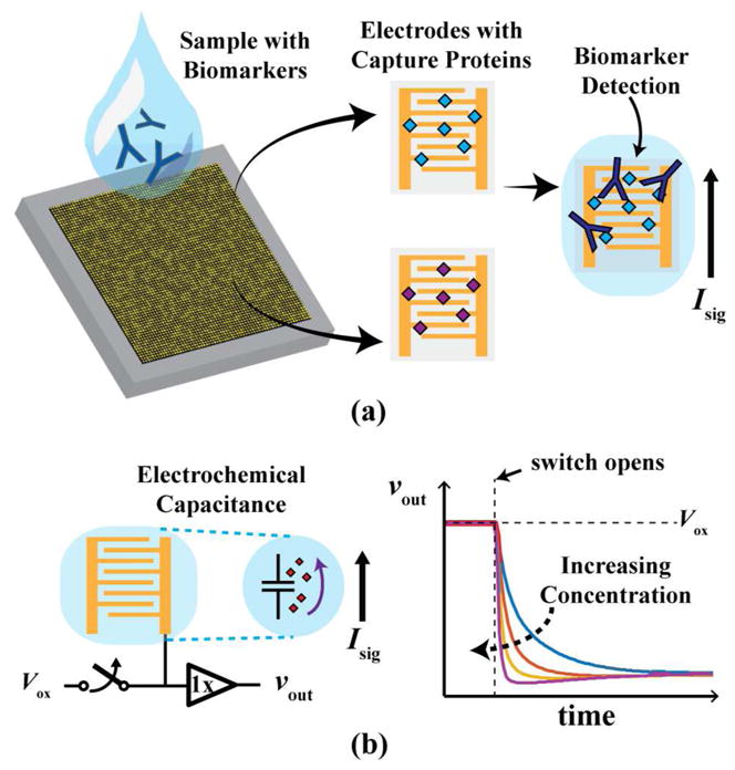
(a) Illustration of a high-density array of electrodes functionalized with multiple capture probes for detecting biomarkers. (b) Coulostatic discharge readout technique used to convert a current into a voltage using the inherent electrochemical capacitance of the sensor.
Current high-density array technologies use optical detection (i.e., fluorescent dyes attached to the analyte) thus requiring complex microarray imaging equipment that is too bulky and impractical for point-of-care (POC) applications where measurements are made in remote areas away from the resources of centralized labs. While electrochemical detection is known to improve the size and scalability of biosensors [5], most implementations still require a potentiostat with an extremely sensitive transimpedance amplifier (TIA) to measure the minute signals associated with microelectrodes, and such designs typically only scale to a ~100×100 μm2 pixel area [6]–[19]. For higher-density implementations, many potentiostat-based arrays either have specially-fabricated sensors to increase sensitivity (i.e., amplify the signal) [10], [20]–[22] or implement parts of the measurement circuitry outside of the array to decrease the pixel size [8], [9]. Nonetheless, neither approach addresses the fundamental difficulty of measuring small currents with decreased sensor size.
In this paper, extended from [23], the design and validation of an integrated high-density biosensor array for vaccination screening, that also enables POC IMS, is presented. It leverages an alternative and little-used electrochemical detection method, coulostatic discharge [23]–[27], to significantly reduce the complexity and size of the readout circuitry. Fig. 1(a) shows an illustration of the array functionalized with different capture proteins to simultaneously detect multiple disease biomarkers. Each biopixel transduces capture events into an electrical signal, Isig(t), whose magnitude is related to the biomarker concentration. Unlike chronoamperometry, where this current is measured directly, the current is used to discharge the sensor’s innate double layer capacitance (Fig. 1b), translating the measurement to changes in vout(t). This technique effectively transforms a miniature current measurement to a much simpler voltage-over-time measurement. As the sensor’s intrinsic capacitance is on the order of tens of pF and Isig(t) is ~1 pA/μM, the discharge rate of vout(t) is on the order of 1 V/s/μM, which greatly relaxes and simplifies the readout circuitry requirements. Hence, this technique along with electrochemical amplification from interdigitated electrodes (IDEs) allows for all the sensors and circuitry to be packed densely enough for high-density array applications using only the features available in a standard CMOS processes.
The remainder of the paper is organized as follows: Section II describes the coulostatic discharge sensing principle, and Section III discusses the design of the biopixel circuitry. Sections IV and V present characterization and biological measurement results, respectively. Comparisons are made in Section VI, and conclusions are drawn in Section VII.
II. Sensing Principle
Coulostatic discharge is an electrochemical technique developed independently by both Reinmuth and Delahay in 1962 that uses the inherent double-layer capacitance between an electrode and an electrolytic solution to convert the signal current to a voltage that changes slowly over time [24], [27]. Specifically, the measurement is performed by charging up this capacitance to a particular voltage and then letting it discharge through the electrochemical cell. To use this method for biomarker detection, the surface of the electrodes must be coated with capture molecules that give the sensor specificity (i.e., the ability to distinguish a specific molecule from others).
The assay steps used in this work are as follows: 1) Each biopixel is functionalized by immobilizing capture proteins on the gold-plated sensor using a standard method of dropcasting an excess amount of proteins to saturate the surface completely. The sensor’s surface is known as the working electrode (WE), which is where the biochemical detection occurs that is subsequently transduced into an electrical signal (Fig. 2a-i). A single sensor contains two WEs separated by an insulating material (e.g., oxide in an IC). Each type of capture protein binds to a specific target antibody due to the binding affinity of the antibody-antigen complex. 2) The biological sample is added to the sensors and incubated so that any antibody biomarkers present in the sample bind to their specific capture protein (Fig. 2a-ii). After washing to remove any unbound molecules, a secondary antibody that binds to the bound antibodies is added to the array, effectively sandwiching the biomarkers (Fig. 2a-iii). This secondary antibody is conjugated with an enzyme, alkaline phosphatase (ALP), that reacts with a p-aminophenyl phosphate (pAPP) substrate, thus generating a by-product redox molecule, p-aminphenyl (pAP), that is detected by the biopixel (Fig. 2a-iv). Detection occurs when pAP approaches a WE biased at a specific voltage, known as the oxidation potential, and reacts to form quinonimine (QI) by transferring electrons to the WE. QI, in turn, reacts at the second working electrode biased at the reduction potential converting back into pAP by receiving electrons. Thus, this shuttling of electrons creates a current proportional to the concentration of the biomarker in the sample. An important distinction to make here is that actual full-scale IMS relies on in-situ printing a large number of randomly-generated peptides onto the array sensors [2], [28]–[30]. To use this array for IMS technology, peptides would be used in place of proteins to detect the antibody profile [31]. The underlying sensing mechanism is the same for both cases, so successful operation of the protein-based assay implies that the array can be used for IMS.
Fig. 2.
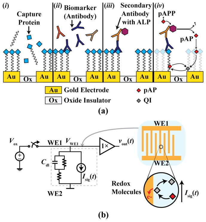
(a) Steps of the antibody detection assay and (b) coulostatic discharge measurement circuit with equivalent sensor model.
The resulting signal would typically be measured directly using standard amperometric techniques and current-based readout circuitry (e.g., as is done in a glucometer). However, in coulostatic discharge, a potential is applied to the electrode only briefly allowing a build-up of charge on the sensor’s intrinsic capacitance, Cdl. This capacitance, known as double layer capacitance, is formed from the layers of ions and charged molecules that assemble at the interface between the electrode and ionic solution, and exists between the electrode and the bulk solution (Fig. 2b). After the source supplying the potential to the electrode is disconnected, Cdl is discharged through the electrochemical cell by the current generated due to the redox reactions, thus slowly decreasing the voltage of the electrode at a rate related to the biomarker concentration.
As implied by Fig. 2(b), near the beginning of the discharge phase the sensor behaves as an RC circuit, where the capacitance is Cdl and the resistance is determined by the initial redox current, which is related to the concentration of the redox molecules. Hence, the discharge rate can be written as
| (1) |
where Isig(t) is the current generated after opening the switch. In practice, the discharge curve is nonlinear due to the voltage dependence of both Isig(t) and Cdl. As described by the Nernst-Planck equation [32], Isig(t) depends on the concentration gradient of the redox molecules around the electrode:
| (2) |
where n is the number of electrons transferred per reaction, F is the Faraday constant, A is the area of the electrode, Do is the diffusion coefficient of the redox molecule, Cox(t) is the concentration of the redox molecule at the electrode surface, and δ is the width of the diffusion layer, which, for microelectrodes, is simply the distance between electrode fingers. Also, the Nernst equation links the voltage of an electrode, i.e., WE1 in Fig. 2, to the concentration of redox molecules at its surface as follows
| (3) |
where E0 is the standard potential of the redox species, R is the universal gas constant, T is the absolute temperature, and Cox,lim is the total concentration of the oxidant and reductant at the electrode surface [33]. Furthermore, the capacitance Cdl is also a function of the electrode voltage. Specifically, Cdl is given by
| (4) |
where ε0εr is the dielectric constant, λD is the Debye length, which is a measure of how far the electric field extends into the solution, kT/q is the thermal voltage, and VWE is the potential of the electrode [32]. Note that the presence of Cdl, which is on the order of 10 pF - 1 nF, obviates the need for an explicit capacitor in each biopixel. This capacitance is also at least one order of magnitude larger than the capacitance formed by the metal electrodes alone, so it dominates the sensor capacitance.
Fig. 3(a) shows simulated discharge curves obtained using (2)–(4) and known redox coefficients. Due to the nonlinear nature of these curves, the optimum range at which to sample the voltage signal is not obvious. To examine the tradeoffs of different sampling times, a noise model of the biopixel including the buffer and sensor’s equivalent noise contributions, ib,n(t) and ie,n(t), is shown in Fig. 3(b), where the noise only affects the measurement after the switch is open. As the measurements are taken by subtracting two samples of the buffer’s output taken at different times (i.e., right after the switch opens and after a certain amount of time), thus implementing correlated double sampling [34], the buffer in this model is connected only to the sensor. Also, charge injection is cancelled by measuring this difference.
Fig. 3.
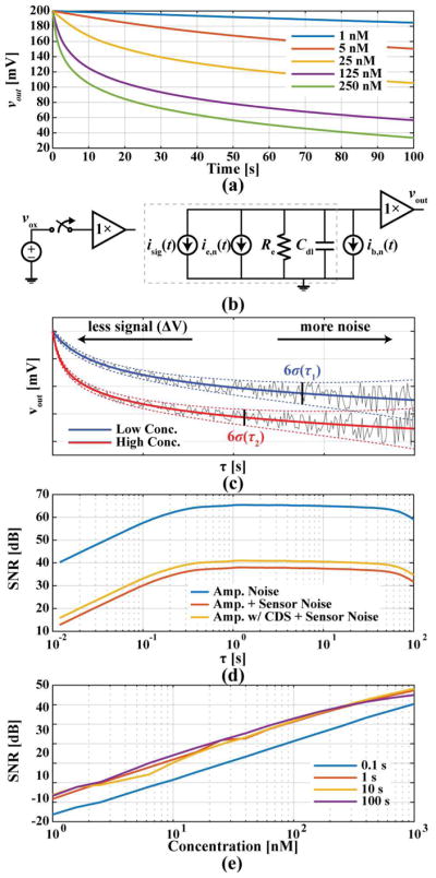
(a) Simulated discharge curves, (b) noise circuit model of pixel, (c) illustration of sampling time tradeoffs, (d) SNR at different sampling times with various noise sources included at a concentration of 100 nM, and (e) SNR in a range of concentrations at various τ.
As described above, Isig(t) integrates onto Cdl, thus creating the characteristic discharge curves illustrated in Fig. 3(a). The sensor’s impedance is modelled as Cdl in parallel with the charge transfer resistance, Rct, which is a measure of how readily the sensor surface reacts with the redox molecules. It follows from Fig. 3(b) and the previous discussion that the voltage noise power can be computed as
| (5) |
where τ is the time at which the buffer output is measured, Se,n(f) and Sb,n(f) are the one-sided power spectral densities (PSDs) of the noise current signals of the sensor and buffer, respectively, and Cdl is assumed to be constant. The noise contributed by the sensor is highly dependent on several biological and chemical factors. Measurement results show that this noise source, which can be modeled as having a white component and a 1/f component, is considerably more dominant than the noise contributed by the buffer, so the buffer design in this system is practically constrained only by the biopixel area.
As shown in Fig. 3(c), for large values of τ the signal component in vout(τ) increases, but the noise variance also increases due to both the white and 1/f components of Se,n(f). In contrast, for small values of τ the signal component in vout(τ) decreases, but the 1/f noise barely affects the measurement. Therefore, a range of suitable sampling times as well as an optimal point that maximizes the signal-to-noise ratio (SNR) can be found. Using estimated values for Rct and Cdl, as well as measured noise PSDs for the buffer and sensor, the noise variance for different values of τ between 10 ms and 100 s was computed. The computed SNR for a 100 nM concentration for different scenarios is shown in Fig. 3(d). As it can be seen from the figure, the SNR is maximized at τ ≅ 1.2 s.
Fig. 3(e) shows that the same trend exists across various concentrations. Depending on the desired resolution, concentration range, and targeted measurement speed, the sampling time, τ, can be reduced. For instance, in applications such as IMS, where coarse or even binary detection is sufficient, a smaller sampling time can be chosen to decrease the time required to scan an entire array. Also, by relating the noise level back to current using Cdl and the sampling time, a current of ~600 fA is expected at τ ≅ 1 s, so the switch should have a leakage smaller than this value.
III. System Design
A. Architecture
Fig. 4 shows a block diagram of the implemented biosensor array, where VWE1 and VWE2 are the input voltages applied to the working electrodes WE1 and WE2, respectively, v1, v2, …, v64 are the array outputs, and the readout circuit below each biopixel comprises a unity-gain buffer and a low-leakage switch controlled by the digital signals r and re. As each vi output is shared among the 64 pixels from its respective column, a 6-bit decoder with outputs d1, d2, …, d64 is used to select the row of the array whose buffer outputs are connected to the array outputs. Given that all the buffers in a column are connected to the same output, the higher the biopixel is in the array, the longer the routing to the output pad is, so the signal sees a different delay to the output depending on the position of the biopixel. However, due to the slow-varying nature of the coulostatic discharge technique, these delays negligibly affect the measurements and are accounted for in the settling time. Nonetheless, in larger arrays, where the number of biopixels might force the use of smaller sampling times, this issue might need to be addressed. In such cases, this problem could be circumvented by dividing the array into subsections with separate outputs, so that the biopixel-to-output-pad paths are more uniform across the array.
Fig. 4.
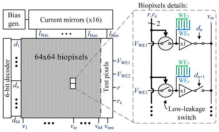
Simplified block diagram of the chip.
The working electrode WE2 is shared by all the pixels within the array, and it is always connected to VWE2. In contrast, each biopixel has its own WE1, and VWE1 is applied to this electrode only when the low-leakage switch is closed. Not shown in the figure are the counter electrode, implemented as a wide gold-plated strip across the center of the array, and the reference electrode, an external Ag/AgCl wire. Together, these electrodes, controlled by off-chip circuitry for flexibility, set the potential of the solution and provide a common reference voltage for the WEs.
A bias current is generated by a constant-gm reference located at the corner of the array and an off-chip resistor. This current is copied to 16 current mirrors at the top of the array, and each distributes this current down the columns to 16 local bias-voltage generators along the length of the chip. Each one of these bias-voltage generators (256 in total), biases the buffers of a 4×4 quadrant of biopixels to reduce area overhead.
To assess the performance of the low-leakage switch, test pixels were implemented on the right side of the array with a dedicated output, vtest. Each one of such pixels is almost identical to an array’s biopixel, but instead of having an IDE connected to the input of its buffer, it has a MIM capacitor of 100 fF, 1 pF or 10 pF size with its other terminal connected to ground. Instead of a low-leakage switch, some of these test pixels have a standard switch consisting of a PMOS transistor with its body tied to the supply voltage.
B. Sensor Design
Since IMS arrays of 330,000 pixels have been shown to be able to diagnosis multiple illnesses reliably, the eventual target number of sensors for a future full-sized electrochemical IMS array is on the order of 100,000. Therefore, assuming the array is fabricated using the full reticle size and that 10% is used for control and output circuitry overhead, the maximum size for each pixel would be ~100×100 μm2. Specifically, an area of 42×42 μm2 per sensor would allow for an array of exactly 330,000 pixels. Guided by this analysis, the electrode geometries were designed using similar pixel areas and constrained by the minimum width and spacing rules of the process.
The microelectrode sensors were fabricated using the top metal layer. Each biopixel consists of two interdigitated electrodes designed to amplify the signal using an electrochemical amplification technique known as redox cycling. Redox cycling is the effect when a reversible redox pair repeatedly diffuses between two electrodes biased at different potentials, one at the reduction potential and the other at the oxidation potential of the pair, transferring electrons through redox reactions at the two electrodes. Hence, a single redox molecule can contribute multiple times to the overall current. The redox current signal, Irc, obtainable from a planar IDE is given by the following empirical equation:
| (6) |
where W and G are the finger width and the gap between fingers, respectively, and
| (7) |
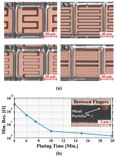
where N is the number of fingers and b is length of the fingers [35]–[38]. It follows from (6) that for a given area, a smaller gap width and a larger number of fingers provide higher amplification. As shown in Fig. 5, four different electrode designs were fabricated. Electrodes A.1 and A.2 have finger and gap widths of 5 μm and 5 μm, whereas electrodes B.1 and B.2 have finger and gap widths of 2 μm and 3 μm. In a standard phosphate buffered saline (PBS) buffer solution, the Cdl of these designs range from 24 to 180 pF. According to (6), the amplification factors of A.1, A.2, B.1 and B.2 are 2.25×, 5.27×, 4.93×, and 9.41×, respectively. Given that (6) is strictly applicable to two-dimensional IDE geometries, the estimated amplification factors are expected to underestimate the measured values.
Fig. 5.
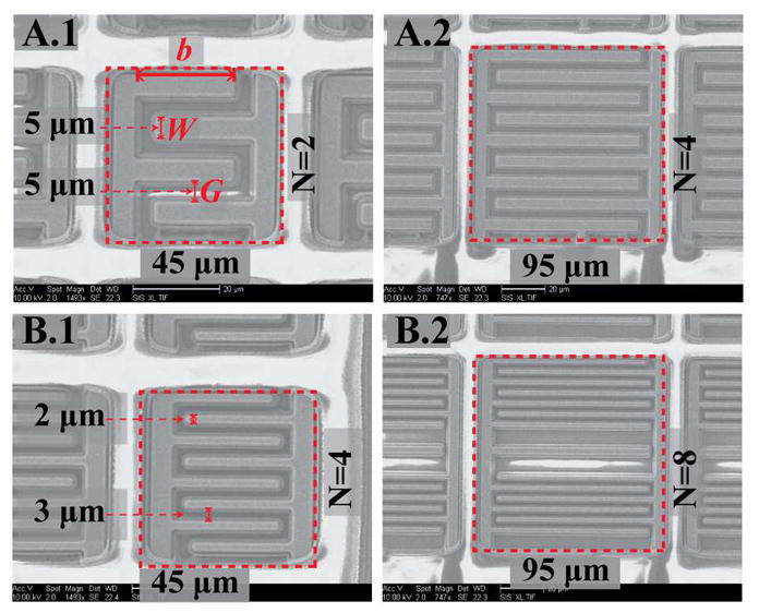
SEM images of the different IDE designs. Both the A and B designs (left and right) have the same finger width and spacing.
Often, physical channels, trenches, and walls are fabricated directly on top of or around the sensor to increase the cycling efficiency, which is a measure of a sensor’s ability to keep the same redox molecules shuttling between the two electrodes without them diffusing away from the sensing area [20], [21], [35]. While these structures are all effective in increasing the amplification, they require complex and customized post-processing steps, thus making the fabrication more time consuming and expensive. To avoid these additional complex post-processing steps while still increasing the signal amplification, an alternative approach that is CMOS foundry compatible was taken. Specifically, the passivation layer directly above each sensor was removed to create 3D structures. By waiving design rule check errors meant to protect the bottom layers of the chip from over etching (the top metal is often used as an etch stop), structures that take advantage of the height of the electrodes were created. Given that the passivation was opened across the entire IDE, the etchant can carve down the gaps between the fingers. As shown in Fig. 6(a), this allows for the formation of 3D trenches between the two electrodes that increase the collection efficiency by trapping the redox molecules and further amplifying the signal. Moreover, as seen in Fig. 6(b), due to the existence of walls left over by the removal of passivation between pixels, effective nanowells were created that isolate the sensors and contain the redox active molecules generated during the assay.
Fig. 6.
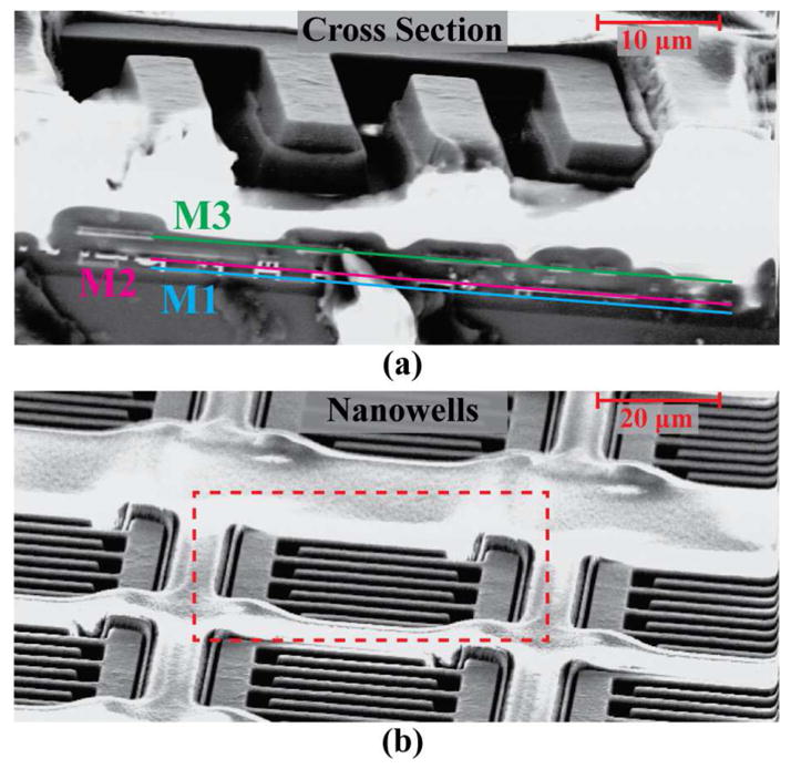
SEM images of (a) chip cross section showing trenches between fingers and (b) nanowells surrounding each pixel.
C. Biopixel Circuitry
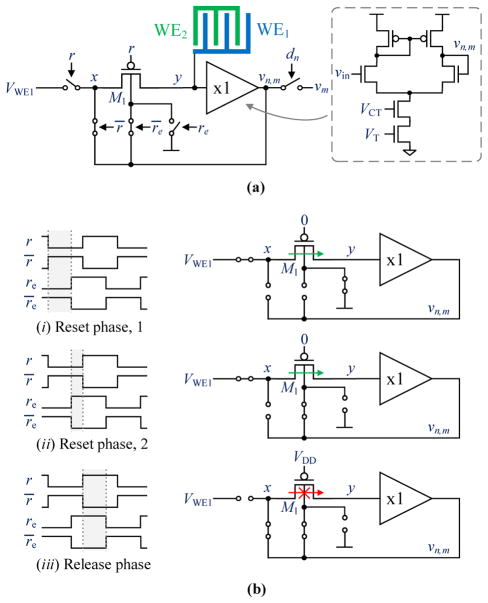
The details of the readout circuit beneath each biopixel are shown in Fig. 7(a). It consists of a low-leakage switch and a unity-gain buffer. To save circuit area, the buffer is used both to read out the voltage of the electrode, vn,m, and to assist the operation of the switch by driving the body of the right-most PMOS transistor when the switch is open. PMOS devices were chosen for the switch to allow for the low-leakage design to be used in any standard CMOS process where individual control of the NMOS body is not possible. The entire circuitry fits underneath the 45×45 μm2 sensor using only three metal layers for routing and one metal layer for the electrodes.
Fig. 7.
(a) Biopixel readout circuit. (b) Ultra-low-leakage switch operation. The frequency of the reset signals is 1 Hz with reset early leading by 1 μs.
The buffer is implemented as a differential amplifier with a cascoded tail transistor. It has 42.8 dB gain and a 26 kHz unity gain bandwidth product. Due to both the switch being PMOS and the voltages used to control the WEs, the input devices of the buffer were required to be NMOS. To minimize the 1/f noise contribution of the buffer, these transistors were made as large as possible given the limited area available.
The low-leakage switch is driven by the digital signals reset, r, and reset-early, re. It comprises of four PMOS transistors with their bodies tied to VDD, illustrated as switches in Fig. 7(a), and a body-driven PMOS transistor, M1 [20], [39]. To minimize the leakage current through M1 when the working electrode WE1 is discharging, both the node labeled as x and the body of M1 are connected to the buffer output, so ideally the PN junctions of M1 see no voltage drop and thus have no leakage current.
The low-leakage switch operation is illustrated in Fig. 7(b). Three phases of operation are distinguished: (i) reset phase 1, (ii) reset phase 2, and (iii) release phase. During (i), M1 is on and the node labeled as y is charged to VWE1. During (ii), M1 is still on, but its body connection is switched from VDD to the buffer output. This is done before M1 is turned off to avoid any charge injection from M1’s channel to node y. Then, during (iii), M1 is turned off and node y starts discharging through the electrodes. Given that both the body of M1 and node x are being driven by the buffer during this phase, the voltage difference between the source, drain, and body terminals of M1 are ideally zero, so that the leakage current is minimized. In practice, the buffer’s offset voltage causes a small voltage drop across the body of M1 and node y, but simulation and measurement results suggest that this is not a problem in practice. For the assay measurement tests, the frequency of the reset signals is set to 1 Hz with re leading r by 1 μs. When measuring the output of the buffer during the release phase, the first and final points are measured at 1 μs and τ after the switch opens.
IV. Characterization Measurements
A 5×5 mm2 chip (Fig. 8) was fabricated in a 1P4M 180 nm CMOS SOI process. The array contains 64×64 biopixels split into four quadrants, each with a different IDE design. Each unit biopixel is only 45×45 μm2.
Fig. 8.
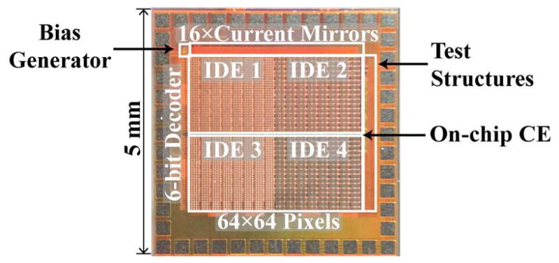
Chip photograph.
A. Electrical Characterization
The entire chip consumes a maximum of 95 mW (23 μW per biopixel) from a 2.5 V supply. The offset of the buffer averaged across the entire array was measured to be 1.78 ± 0.16 mV. The input-referred total integrated noise of the buffer is 33 μVrms (100 kHz bandwidth) with a 1/f noise corner of 120 Hz.
To assess the performance of the low-leakage switch, discharge tests were run using the test pixels. There are two different types of test pixels: one with a standard PMOS switch and the other, which is identical to the one used in the array, with a body-driven switch (Fig. 9a). Separate pixels of each type are attached to known MIM capacitors in place of the top metal electrodes. For each of these tests, up to 0.5 V was placed across the two working electrodes. Just as in a normal discharge test, the switch opens and charge begins to leak from the capacitor into the switch causing the voltage measured to decrease over time. The slope of the measured voltage over time and the known capacitance size was then used to calculate the leakage current the test sensor experiences. The body-driven switch leakage was measured to be 13 aA, which is less than that of the standard PMOS switch with the body tied to VDD, which was 195 aA (Fig. 9b). The body-driven switch had better performance across the entire voltage range.
Fig. 9.
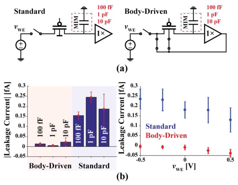
(a) Test pixel schematics. (b) Average leakage measurement results from the test structures with 0.5 V applied across each (left) and the average leakage of all the test structures at different sensor voltages (n = 3).
The results suggest that a standard switch could be used instead of a low-leakage switch in this application. This is the case because the array was designed in an SOI process. However, the biopixel topology is meant to be used in different processes, where standard switches might not perform as well. For instance, in a standard 180 nm process, according to simulations, the leakage current of a typical PMOS switch is ~1.3 pA, whereas that of the low-leakage switch is ~4 fA.
B. Sensor Preparation
For electrochemical compatibility, an electroless nickel immersion gold (ENIG) plating process (MICRO, Stapleton Technologies Inc.) was used to plate the exposed top metal aluminum electrodes [7], [12], [40], [41]. After a thorough cleaning of the surface with acid, akaline, and deoxygenation cleaners, the entire chip was put through a double zincate process to prepare the exposed aluminum electrodes for the subsequent electroless nickel and gold plating steps. The SEM images of each sensor after plating are shown in Fig. 10(a). Typically, as with most on-chip electrochemical sensors, it is desirable to maximize the thickness of both the nickel and gold layers in order to achieve reliable adhesion and uniform coverage. The combined thickness of these layers is usually around 3 μm. Since the electrodes in this work are interdigitated instead of a single pad of metal, the spacings and features of the IDEs are small enough that the plating can create unwanted shorts between the two working electrodes. Furthermore, even collections of small metal particles left over from the plating process can cause individual IDEs to have much lower resistances. Hence, different plating times of both the nickel and gold steps were experimented with and evaluated by measuring the resistance between the two halves of the IDE (Fig. 10b). A total plating time of ~5 minutes was found to be optimal due to its high resistance while still maintaining a robust and even coverage of gold across the array.
Fig. 10.
(a) SEM images of each sensor after gold plating colored to show texture. (b) Minimum resistance measured between the working electrodes with different gold plating times. Inset shows metal particles that can provide a low resistance path if plated for an extended period.
C. Electrochemical Characterization
To evaluate the performance of the sensors as well as the gold plating, a chip with bare gold electrodes was used to measure the redox molecule Ferro/Ferricyanide as a proxy for the actual assay. After cleaning the chip by sonicating in isopropyl alcohol, the chip was mounted in a socket designed to create a ~10 μL well over the sensors. External Ag/AgCl and Pt electrodes were dipped into this well to form the reference and counter electrodes. Next, coulostatic discharge was run using the in-pixel circuitry to measure the sensors in various concentrations of Ferri/Ferricyanide in both single working electrode, as seen in Fig. 11(a), and dual working electrode modes to compare the same sensor with and without redox cycling. In single electrode mode, both sides of the IDE are shorted together, instead of biased independently, effectively making them into a single electrode with combined area where no redox cycling can occur. In dual electrode mode, the IDE operates as intended with one electrode biased at 200 mV and the other at 0 mV relative to VCM, allowing for the shuttling of the redox molecules. Using these measurements, the amplification factor was determined by calculating the ratio of the signals between the dual and single electrode modes. As shown in Fig. 11(b), the average amplification factors for each design are 5.33 ± 1.2×, 8.1 ± 1.5×, 6.06 ± 2.1×, and 10.5 ± 2.1×, respectively. These values are slightly larger than the theoretical values due to the 3D trench and nanowell structures. IDEs with the same gap and finger widths but greater number of fingers have higher amplification. Smaller gap size also increases the redox cycling, as expected. Furthermore, the large variation in amplification can be explained as either a result of un-even plating of gold in the trenches or variability in the formation of the trenches themselves. The latter seems more likely since the plating procedure is widely used while the etching between fingers is unconventional and not guaranteed by the foundry.
Fig. 11.
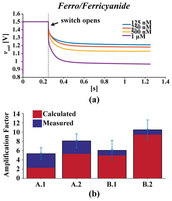
(a) Discharge measurements of combined working electrodes with various concentrations of Ferro/Ferricyanide. (b) Calculated and measured (n = 60) amplification factor using coulostatic discharge.
V. Biological Measurement Results
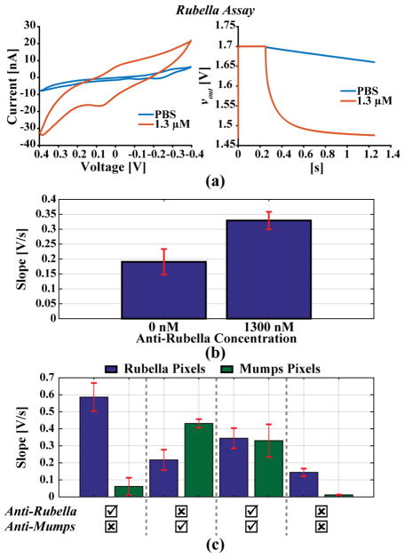
For the biological tests, only a portion of the array that has the same electrode design, A.2, was used to allow for a fair comparison between tests. To demonstrate a bioassay, 2 μg (66 pmol) of Rubella virus capsid protein (ab74574, Abcam) in PBS was dropcast on the surface of the gold sensor array using 20 μg of Traut’s Reagent (26101, ThermoFischer Pierce) and blocked with 1% bovine serum albumin (37525, ThermoFischer Scientific). Mouse anti-Rubella antibodies (ab34749, Abcam) were subsequently added and incubated for one hour. For the secondary antibody, 1 μg of rabbit anti-mouse secondary antibodies linked with ALP (ab6729, Abcam) was used. Lastly, 6 mM pAPP substrate (sc-281392, Santa Cruz Biotechnology) in a 0.1 M glycine buffer pH 8.4 was added and allowed to incubate for ten minutes. The ALP enzyme reacts with the pAPP substrate producing AP, an electrochemically active molecule that shuttles electrons between the two fingers of the sensor. Fig. 12(a) shows measurement results for both CV, measured with a 25 mV/s scan rate from −0.2 V to 0.3 V for 3 cycles, and coulostatic discharge. Both successfully detect the presence of anti-Rubella antibodies. The experiment was then repeated for anti-Rubella spiked into human serum (HS-20, Omega Scientific, Inc.). Fig. 12(b) shows the average discharge rates for serum with and without the antibody.
Fig. 12.
(a) CV and discharge curves for a single electrode compared with a control. (b) Average discharge rate for positive and negative detection of anti-Rubella antibody (n = 30). (c) Discharge rates for multi-antibody detection of both anti-Rubella and anti-Mumps antibodies (n = 8).
Next, a multi-biomarker assay meant to simultaneously detect both anti-Rubella and anti-Mumps (ab9880, Abcam) antibodies was performed using the array. The same portion of the array used for the previous Rubella-only test was split into two, with each part functionalized with either Rubella or Mumps protein (ab74560, Abcam). Four different chips were used for this experiment, all functionalized exactly as described above. Each chip was given a different test sample of serum spiked with 1.3 μM Rubella antibodies, 2.3 μM Mumps antibodies, both, or neither. As seen in Fig. 12(c), the parts of the array that are exposed to their corresponding antibody show a higher slope than those that are not. Although there exists a large chip-to-chip variation, likely due to disparity in functionalization or test conditions between the different chips, the array can still distinguish between each of these different samples to detect the presence of either biomarker, thereby demonstrating its capability to monitor vaccinations.
VI. Comparison
Table I compares this work to other integrated electrochemical biosensor arrays, and Fig. 13 plots their pixel areas and number of devices per pixel with different markers to signify those that have special post-processing and/or have measurement circuitry external to the array. Due to redox cycling, this work achieves a relatively small pixel area and high sensor density (400 pixels/mm2) without any complex post-processing, which others need to increase sensitivity. While augmenting sensors with additional structures and materials is effective, it requires complex fabrication steps that are much more difficult and expensive to produce and scale than an array built purely with a standard CMOS process. To the best of our knowledge, this work is the highest density amperometric biosensor array that does not require additional post-processing steps. Furthermore, coulostatic discharge greatly decreases the number of devices required in the measurement circuitry (~12) allowing for all the circuit to reside completely within the area of a pixel. In fact, the two arrays based on coulostatic discharge have the lowest number of devices that fit completely within a pixel. Hence, rather than occupying a considerable amount of area with circuit blocks external to the array, this work makes efficient use of the chip area as illustrated by the total density calculation in Table I.
TABLE I.
Comparison with State-of-the-Art Integrated Electrochemical Biosensor Arrays
| HASSIBI [6] | MANICKAM [7] | KIM [8] | ROTHE [9] | HALL [20] | NASRI [10] | THIS WORK | |
|---|---|---|---|---|---|---|---|
| Technology (μm) | 0.18 | 0.35 | 0.5 | 0.35 | 0.032 | 0.065 | 0.18 |
| Num. Pixels | 50 | 100 | 100 | 1,024 | 8,192 | 4 | 4,096 |
| Sensor Density [#/mm2] | 52.1 | 69.4 | 1,046 | 100 | 50,000 | 22.2 | 400 |
| Total Density [#/mm2] | 11.90 | 25.00 | 11.11 | 28.44 | 327.68 | 0.44 | 163.84 |
| Electrode Area [μm2] | 3,600 | 1,600 | 225 | 491 | 1 | 5,000 | 2,025 |
| Pixel Area [μm2] | 19,200 | 10,000 | 745 | 10,000 | 20 | 45,000 | 2,500 |
| Devices Per Pixel | 301 | 34 | >9* | 21** | 3 | 37 | 12 |
| Complex Post-Processing? | NO | NO | YES | YES | YES | YES | NO |
| Dual Electrode? | YES | NO | NO | NO | YES | NO | YES |
| Technique | MULT. | EIS | CA | AMP. | CD | FSCV | CD |
MULT – multiple techniques, EIS – Electrochemical Impedance Spectroscopy, CA – Chronoamperometry, Amp. – Amperometry, CD – Coulostatic discharge, FSCV – Fast scan cyclic voltammetry
Part of the measurement circuitry is located outside of the pixel and a 50 fF capacitor and buffer circuit were not included in the device count.
All the measurement circuitry is located outside of the pixel. This is a per row device number.
Fig. 13.
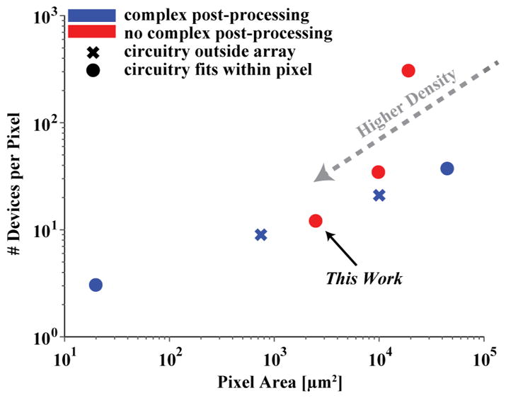
Plot comparing the pixel areas and number of devices per pixel of high-density electrode arrays summarized in Table I.
VII. Conclusion
This paper presents a scalable coulostatic discharge-based high-density biosensor array designed to miniaturize multiple antibody measurement technology. Using coulostatic discharge rather than standard amperometry, the measurement circuitry in each biopixel is simplified to just a low-leakage switch and output buffer, thereby minimizing the overall density and area of the array. Furthermore, by optimizing on-chip IDE geometries and waiving fabrication design rules to create 3D structures, a signal amplification of ~10× was achieved without any complex, costly, and time-consuming post-processing of the sensors. Using this array, Rubella antibody was detected in human serum and simultaneous measurements of both Rubella and Mumps antibodies were possible on the same chip. These tests demonstrate this array’s promise for use in full-scale IMS technology for rapid and accurate point-of-care screening and diagnosis.
Acknowledgments
This work was supported in part by Intel Labs through SRC, the UCSD Medical Devices and Systems (MDS) initiative, the National Institute of Health (Grant R21 AI121914), and the UCSD Center for Aids Research (Grant P30 AI36214).
The authors would like to thank Mentor Graphics for the use of their Analog FastSPICE tool.
Biographies

Alexander C. Sun (S’13) received his B.S. degree in 2012 in Electrical Engineering and Computer Science from the University of California, Berkeley and his M.S. degree in 2014 in Electrical and Computer Engineering from the University of California at San Diego where he is currently pursuing a PhD. His research focus is on electrochemical biosensors, electrochemical measurement techniques, and compact, low power circuit design for biomedical and point-of-care devices.

Enrique Alvarez-Fontecilla received his B.S. and M.S. degrees in Electrical Engineering from Universidad Católica de Chile (PUC), Santiago, Chile, in 2011 and 2013, respectively. He is currently pursuing the Ph.D. degree at the University of California at San Diego. From 2012 to 2015 he worked as an Adjunct Assistant Professor at PUC in both the School of Engineering and the Institute of Philosophy.

A. G. Venkatesh received the B.Sc. degree in biochemistry from the University of Madras, Tamil Nadu, India, the M.Sc. degree in biotechnology from Bharathidasan University, Tamil Nadu, India, the M.Tech. degree in bioelectronics from Tezpur University, Assam, India, and the Ph.D. degree in physics from Bielefeld University, Bielefeld, Germany. During his doctoral research, he developed a novel platform to monitor DNA-protein interactions in real-time and, as a Postdoctoral Researcher at the University of Freiburg, Freiburg im Breisgau, Germany, he developed low-cost, smartphone-based devices for biomedical applications. At the University of California at San Diego, he was involved in developing smartphone-based electrochemical assays for clinical applications in the point-of-care domain. Currently as a Bioelectronic scientist at Roswell Biotechnologies, San Diego, USA, he is developing next generation DNA sequencing biosensor platforms. As an Interdisciplinary Researcher, he is interested in research that involves the integration of physics, chemistry, and biology.

Eliah Aronoff-Spencer received his B.S. degree in Biochemistry with honors from University of California, Santa Cruz, CA, USA in 1998 and MD and PhD Degree in Biophysics in 2006 from Albert Einstein College of Medicine, Bronx, New York. From 2005–2006 he was an AECOM Global health fellow working primarily in South Africa. He completed the Physician Scientist Training Program at the University of California at San Diego, CA, USA in 2013, with Double Board Certification in Internal Medicine and Infectious Diseases and post-doctoral training in Bioinformatics. He Joined the UC San Diego faculty in 2014 where he is Assistant Professor of Medicine in the Division of Infectious Diseases and Global Public Health. He is the Director of the Center for Health Design at the UCSD Design Lab, and Co-director of Distributed Health Labs at the Qualcomm Institute.

Drew A. Hall (S’07--M’12) received the B.S. degree in computer engineering with honors from the University of Nevada, Las Vegas, NV, USA, in 2005, and the M.S. and Ph.D. degrees in electrical engineering from Stanford University, Stanford, CA, USA, in 2008 and 2012, respectively.
From 2011 to 2013, he was a Research Scientist in the Integrated Biosensors Laboratory at Intel Corporation. Since 2013, he has been with the Department of Electrical and Computer Engineering, University of California at San Diego, as an Assistant Professor. His research interests include bioelectronics, biosensors, analog circuit design, medical electronics, and sensor interfaces.
Dr. Hall received the First Place in the Inaugural International IEEE Change the World Competition and First Place in the BME-IDEA invention competition, both in 2009. He received the Analog Devices Outstanding Designer Award in 2011, an Undergraduate Teaching Award in 2014, the Hellman Fellowship Award in 2014, and an NSF CAREER Award in 2015. He is also a Tau Beta Pi Fellow. He has served as an Associate Editor of the IEEE TRANSACTIONS ON BIOMEDICAL INTEGRATED CIRCUITS since 2015 and has been a member of the CICC Technical Program Committee since 2017.
Contributor Information
Alexander C. Sun, Electrical and Computer Engineering Department, University of California, San Diego, La Jolla, CA 92093 USA.
Enrique Alvarez-Fontecilla, Electrical and Computer Engineering Department, University of California, San Diego, La Jolla, CA 92093 USA.
A. G. Venkatesh, Electrical and Computer Engineering Department, University of California, San Diego, La Jolla, CA 92093 USA
Eliah Aronoff-Spencer, School of Medicine, University of California, San Diego, La Jolla, CA 92093 USA.
Drew A. Hall, Electrical and Computer Engineering Department, University of California, San Diego, La Jolla, CA 92093 USA.
References
- 1.Stafford P, Cichacz Z, Woodbury NW, Johnston SA. Immunosignature system for diagnosis of cancer. Proc Natl Acad Sci. 2014 Jul;111(30):E3072–E3080. doi: 10.1073/pnas.1409432111. [DOI] [PMC free article] [PubMed] [Google Scholar]
- 2.Legutki JB, Zhao Z-G, Greving M, Woodbury N, Johnston SA, Stafford P. Scalable high-density peptide arrays for comprehensive health monitoring. Nat Commun. 2014 Sep;5 doi: 10.1038/ncomms5785. [DOI] [PubMed] [Google Scholar]
- 3.Legutki JB, Johnston SA. Immunosignatures can predict vaccine efficacy. Proc Natl Acad Sci U S A. 2013 Nov;110(46):18614–18619. doi: 10.1073/pnas.1309390110. [DOI] [PMC free article] [PubMed] [Google Scholar]
- 4.Restrepo L, Stafford P, Johnston SA. Feasibility of an early Alzheimer’s disease immunosignature diagnostic test. J Neuroimmunol. 2013 Jan;254(1–2):154–160. doi: 10.1016/j.jneuroim.2012.09.014. [DOI] [PubMed] [Google Scholar]
- 5.Roda A, Michelini E, Zangheri M, Di Fusco M, Calabria D, Simoni P. Smartphone-based biosensors: A critical review and perspectives. TrAC Trends Anal Chem. 2016 May;79:317–325. [Google Scholar]
- 6.Hassibi A, Lee TH. A programmable electrochemical biosensor array in 0.18 μm standard CMOS. ISSCC. 2005 IEEE International Digest of Technical Papers. Solid-State Circuits Conference, 2005; 2005; pp. 564–617. [Google Scholar]
- 7.Manickam A, Chevalier A, McDermott M, Ellington AD, Hassibi A. A CMOS electrochemical impedance spectroscopy biosensor array for label-free biomolecular detection. 2010 IEEE International Solid-State Circuits Conference - (ISSCC); 2010; pp. 130–131. [Google Scholar]
- 8.Kim BN, Herbst AD, Kim SJ, Minch BA, Lindau M. Parallel recording of neurotransmitters release from chromaffin cells using a 10×10 CMOS IC potentiostat array with on-chip working electrodes. Biosens Bioelectron. 2013 Mar;41:736–744. doi: 10.1016/j.bios.2012.09.058. [DOI] [PMC free article] [PubMed] [Google Scholar]
- 9.Rothe J, Frey O, Stettler A, Chen Y, Hierlemann A. Fully Integrated CMOS Microsystem for Electrochemical Measurements on 32 × 32 Working Electrodes at 90 Frames Per Second. Anal Chem. 2014 Jul;86(13):6425–6432. doi: 10.1021/ac500862v. [DOI] [PMC free article] [PubMed] [Google Scholar]
- 10.Nasri B, et al. 15.7 Heterogeneous integrated CMOS-graphene sensor array for dopamine detection. 2017 IEEE International Solid-State Circuits Conference (ISSCC); 2017; pp. 268–269. [Google Scholar]
- 11.Ghoreishizadeh SS, Georgiou P, Carrara S, Micheli GD. An integrated platform for differential electrochemical and ISFET sensing. 2016 IEEE International Symposium on Circuits and Systems (ISCAS); 2016; pp. 2875–2878. [Google Scholar]
- 12.Niitsu K, Ota S, Gamo K, Kondo H, Hori M, Nakazato K. Development of Microelectrode Arrays Using Electroless Plating for CMOS-Based Direct Counting of Bacterial and HeLa Cells. IEEE Trans Biomed Circuits Syst. 2015 Oct;9(5):607–619. doi: 10.1109/TBCAS.2015.2479656. [DOI] [PubMed] [Google Scholar]
- 13.Chen Y, et al. CMOS high density electrical impedance biosensor array for tumor cell detection. Sens Actuators B Chem. 2012 Oct;173:903–907. [Google Scholar]
- 14.Li L, Liu X, Qureshi WA, Mason AJ. CMOS Amperometric Instrumentation and Packaging for Biosensor Array Applications. IEEE Trans Biomed Circuits Syst. 2011 Oct;5(5):439–448. doi: 10.1109/TBCAS.2011.2171339. [DOI] [PubMed] [Google Scholar]
- 15.Yang C, Huang Y, Hassler BL, Worden RM, Mason AJ. Amperometric Electrochemical Microsystem for a Miniaturized Protein Biosensor Array. IEEE Trans Biomed Circuits Syst. 2009 Jun;3(3):160–168. doi: 10.1109/TBCAS.2009.2015650. [DOI] [PubMed] [Google Scholar]
- 16.Levine PM, Gong P, Levicky R, Shepard KL. Active CMOS Sensor Array for Electrochemical Biomolecular Detection. IEEE J Solid-State Circuits. 2008 Aug;43(8):1859–1871. [Google Scholar]
- 17.Ayers S, Gillis KD, Lindau M, Minch BA. Design of a CMOS Potentiostat Circuit for Electrochemical Detector Arrays. IEEE Trans Circuits Syst Regul Pap. 2007;54(4):736–744. doi: 10.1109/TCSI.2006.888777. [DOI] [PMC free article] [PubMed] [Google Scholar]
- 18.Thewes R, et al. Sensor arrays for fully-electronic DNA detection on CMOS. 2002 IEEE International Solid-State Circuits Conference; 2002; pp. 350–473. [Google Scholar]
- 19.Augustyniak M, et al. A 24×16 CMOS-Based Chronocoulometric DNA Microarray. 2006 IEEE International Solid State Circuits Conference - Digest of Technical Papers; 2006; pp. 59–68. [Google Scholar]
- 20.Hall DA, et al. 16.1 A nanogap transducer array on 32nm CMOS for electrochemical DNA sequencing. 2016 IEEE International Solid-State Circuits Conference (ISSCC); 2016; pp. 288–289. [Google Scholar]
- 21.Ma C, Contento NM, Bohn PW. Redox Cycling on Recessed Ring-Disk Nanoelectrode Arrays in the Absence of Supporting Electrolyte. J Am Chem Soc. 2014 May;136(20):7225–7228. doi: 10.1021/ja502052s. [DOI] [PubMed] [Google Scholar]
- 22.Ino K, et al. Densified Electrochemical Sensors Based on Local Redox Cycling between Vertically Separated Electrodes in Substrate Generation/Chip Collection and Extended Feedback Modes. Anal Chem. 2014 Apr;86(8):4016–4023. doi: 10.1021/ac500435d. [DOI] [PubMed] [Google Scholar]
- 23.Sun A, Alvarez-Fontecilla E, Venkatesh AG, Aronoff-Spencer E, Hall DA. A 64×64 High-Density Redox Amplified Coulostatic Discharge-Based Biosensor Array in 180nm CMOS. presented at the ESSCIRC 2017; Leuven, Belgium. 2017; [DOI] [PMC free article] [PubMed] [Google Scholar]
- 24.Reinmuth WH, Wilson CE. An Impulse (Coulostatic) Relaxation Method for the Study of Rapid Electrode Processes. Anal Chem. 1962 Aug;34(9):1159–1161. [Google Scholar]
- 25.Zhu X, Ahn CH. On-Chip Electrochemical Analysis System Using Nanoelectrodes and Bioelectronic CMOS Chip. IEEE Sens J. 2006 Oct;6(5):1280–1286. [Google Scholar]
- 26.Sun A, Au A, Venkatesh AG, Gilja V, Hall DA. A scalable high-density electrochemical biosensor array for parallelized point-of-care diagnostics. 2015 IEEE Biomedical Circuits and Systems Conference (BioCAS); 2015; pp. 1–4. [Google Scholar]
- 27.Delahay P. Coulostatic Method for the Kinetic Study of Fast Electrode Processes. I. Theory. J Phys Chem. 1962 Nov;66(11):2204–2207. [Google Scholar]
- 28.Halperin RF, Stafford P, Johnston SA. Exploring Antibody Recognition of Sequence Space through Random-Sequence Peptide Microarrays. Mol Cell Proteomics MCP. 2011 Mar;10(3) doi: 10.1074/mcp.M110.000786. [DOI] [PMC free article] [PubMed] [Google Scholar]
- 29.Brown JR, Stafford P, Johnston SA, Dinu V. Statistical methods for analyzing immunosignatures. BMC Bioinformatics. 2011 Aug;12:349. doi: 10.1186/1471-2105-12-349. [DOI] [PMC free article] [PubMed] [Google Scholar]
- 30.Breitling F, Nesterov A, Stadler V, Felgenhauer T, Bischoff FR. High-density peptide arrays. Mol Biosyst. 2009 Feb;5(3):224–234. doi: 10.1039/b819850k. [DOI] [PubMed] [Google Scholar]
- 31.Legutki JB, Magee DM, Stafford P, Johnston SA. A general method for characterization of humoral immunity induced by a vaccine or infection. Vaccine. 2010 Jun;28(28):4529–4537. doi: 10.1016/j.vaccine.2010.04.061. [DOI] [PubMed] [Google Scholar]
- 32.Bard Allen J, Faulkner Larry R. Electrochemical Methods Fundamentals and Applications. 2. Wiley; 2001. [Google Scholar]
- 33.Zhu X, Choi J-W, Ahn CH. A new dynamic electrochemical transduction mechanism for interdigitated array microelectrodes. Lab Chip. 2004 Nov;4(6):581–587. doi: 10.1039/b407930b. [DOI] [PubMed] [Google Scholar]
- 34.Avila D, Alvarez E, Abusleme A. Noise Analysis in Pulse-Processing Discrete-Time Filters. IEEE Trans Nucl Sci. 2013 Dec;60(6):4634–4640. [Google Scholar]
- 35.Dam VaT, Olthuis W, van den Berg A. Redox cycling with facing interdigitated array electrodes as a method for selective detection of redox species. Analyst. 2007 Mar;132(4):365–370. doi: 10.1039/b616667a. [DOI] [PubMed] [Google Scholar]
- 36.Min J, Baeumner AJ. Characterization and Optimization of Interdigitated Ultramicroelectrode Arrays as Electrochemical Biosensor Transducers. 2004:724–729. [Google Scholar]
- 37.Paeschke M, Wollenberger U, Köhler C, Lisec T, Schnakenberg U, Hintsche R. Properties of interdigital electrode arrays with different geometries. Anal Chim Acta. 1995 Apr;305(1–3):126–136. [Google Scholar]
- 38.Aoki K, Morita M, Niwa O, Tabei H. Quantitative analysis of reversible diffusion-controlled currents of redox soluble species at interdigitated array electrodes under steady-state conditions. J Electroanal Chem Interfacial Electrochem. 1988 Dec;256(2):269–282. [Google Scholar]
- 39.Su JJ, Demirci KS, Brand O. A Low-Leakage Body-Guarded Analog Switch in 0.35- BiCMOS and Its Applications in Low-Speed Switched-Capacitor Circuits. IEEE Trans Circuits Syst II Express Briefs. 2015 Oct;62(10):947–951. [Google Scholar]
- 40.Ota S, Niitsu K, Kondo H, Hori M, Nakazato K. A CMOS sensor platform with 1.2 μm × 2.05 μm electroless-plated 1024 × 1024 microelectrode array for high-sensitivity rapid direct bacteria counting. 2014 IEEE Biomedical Circuits and Systems Conference (BioCAS) Proceedings; 2014. pp. 460–463. [Google Scholar]
- 41.Hwang S, LaFratta CN, Agarwal V, Yu X, Walt DR, Sonkusale S. CMOS Microelectrode Array for Electrochemical Lab-on-a-Chip Applications. IEEE Sens J. 2009 Jun;9(6):609–615. [Google Scholar]


