Abstract
Multimode interference (MMI) waveguides can be used to create wavelength-dependent spot patterns which enables simultaneous analyte detection on a single optofluidic chip, useful for disease diagnostics. The fidelity of such multi-spot patterns is important for high sensitivity and accurate target identification. Buried rib structures have been incorporated into these SiO2-based waveguides to improve environmental stability. Through experiments and simulation, this letter explores design parameters for a buried MMI rib waveguide based on anti-resonant reflecting optical waveguides in order to produce high-fidelity spot patterns. Optimal rib heights and widths are reported in the context of available microfabrication etch technology and performance for an optimized biosensor is shown.
Keywords: Biophotonics, biosensors, dielectric waveguides, fluorescence spectroscopy, integrated optics, multimode interference waveguides, multiplexing
I. INTRODUCTION
OPTOFLUIDIC devices for use in lab-on-a-chip systems are being developed for applications such as chemical screening, genomic sequencing, and analyte detection for clinical diagnostics [1], [2]. In recent years the push for clinical diagnostics has been expedited to address threats like the global outbreaks of Ebola hemorrhagic fever and Zika virus and the growing need for rapid detection and analysis of antibiotic resistance in bacteria [3]–[5]. In order for chip-based systems to reach required limits of detection (LOD) they must be sensitive to targets (e.g. DNA strands, proteins, or viruses) labeled with as few fluorescing molecules as possible. In addition, optofluidic systems need the ability to multiplex so that multiple targets can be detected simultaneously. A simple passive photonic device capable of optofluidic multiplexing is the MMI waveguide, which has been widely developed for use in telecommunications for its ability to split and combine optical signals. The MMI waveguide has a small footprint and was recently implemented for optofluidic multiplexing [6].
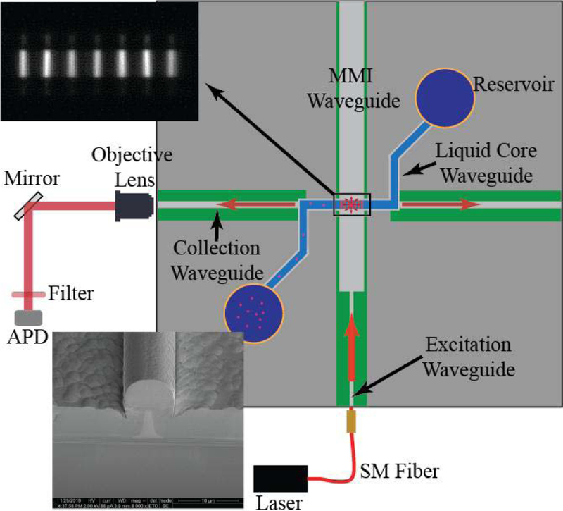
Multiplexing capabilities and sensitivity enhancements have already been shown for a liquid core anti-resonant reflecting optical waveguide (LC-ARROW) platform [6], [7]. As seen in Fig. 1, the platform passes bioparticles orthogonally through an MMI excitation pattern, which consists of N equally spaced spots. The number of spots N is wavelength dependent giving the sensor its ability to multiplex. Standard fluorescent dyes which fluoresce at specific wavelengths are used to selectively label genetic markers, such as DNA strands. As labeled molecules pass the spot pattern they can be identified by the generated number of fluorescence peaks. The acquired signal can be enhanced through a simple signal processing algorithm to provide increased signal-to-noise ratios (SNRs) [7], [8]. This algorithm multiplies the collected fluorescence signal shifted by a multiple of the time between peaks T. For the spot pattern to be considered “high-fidelity”, individual spots should be of uniform intensity, narrow, and clearly separated without background illumination between neighboring spots. The single-mode excitation waveguides used to excite the MMI waveguide are critical, as their geometry determines the size of the mode to be self-imaged in the MMI waveguide’s output.
Fig. 1.

Representation of the LC-ARROW optofluidic platform under test. (Top Left Inset) Top view image of the MMI waveguides spot pattern generated at an excitation wavelength of λ = 633 nm and liquid core filled Cy-5 fluorophores. (Bottom Left Inset) SEM image of the excitation waveguide’s facet, which shows the buried rib structure. The rib structure is highlighted for print visibility.
In this letter, we concentrate on optimizing the buried rib excitation waveguide’s structural geometry and demonstrate how they affect the fidelity of resulting excitation spot patterns and subsequent fluorescence signals. The buried design is necessary to reduce water absorption in the rib structure. Water absorption reduces mode confinement in the excitation waveguide and is detrimental to the MMI waveguide’s excitation pattern [9], [10].
II. PLATFORM CONSTRAINTS
The purpose of this section is to discuss the constraints inherent in the optofluidic platform that limits the MMI waveguide’s design parameters. The optofluidic platform has already proven capable of simultaneous identification of various biomarkers, including labeled DNA strands and single viruses [6], [11], [12]. These results were attained with standard single-oxide rib waveguide design which produced less than optimal high-fidelity spot patterns. For the sensor to surpass previous limits in sensitivity, high-fidelity spot patterns from the MMI waveguide are prerequisite.
The platform, as illustrated in the top view image of Fig. 1, consists of an MMI waveguide which intersects a liquid core between 5 and 6 μm tall and 12 μm wide. For the excitation modes to pass through the core at the optimum height and to provide structural integrity to the hollow channel, 6 μm of plasma enhanced chemical vapor deposited (PECVD) oxide is deposited as the optical guiding layer forming the walls of the liquid core. PECVD SiO2 (nc = 1.51) is attractive as a guiding layer in our system as it can be deposited at low temperatures, achieves high thicknesses and has a low photoluminescence in the visible regime. PECVD SiO2 is hygroscopic because of its low deposition temperatures. To prevent water absorption in the core, another 6 μm of PECVD oxide (nc = 1.45) is deposited to form a top cladding layer [10], [13]. This comes at the cost of a reduced refractive index contrast of 3.9%, which fundamentally widens the mode compared to a non-buried rib waveguide of the same geometry [14], [15].
The reduced index contrast of the new buried structure also widens the effective width weff of the MMI waveguide. The geometry of the MMI waveguide is governed by
where nc is the refractive index of the core, L the length of the MMI waveguide, N the number of self-imaged spots, and λ the wavelength of excitation light [14]. In order to enable optofluidic multiplexing over various wavelengths, the MMI was designed to produce N = 7 spots at 633 nm, N = 8 spots at 556 nm and N = 9 at 488 nm. At these colors, the chosen fluorescent dyes are excited at their wavelengths of maximum absorption and the excitation beams are properly removed by a single penta-bandpass filter prior to being collected by a single-photon counting avalanche photodiode. The tight band dλ constraints from aligning emission wavelengths with the filter inflict strict fabrication tolerances on the width of the MMI waveguide. In order to fit within the required wavelength range, MMI widths must be accurate to +/ − 0.8% of target widths [14]. Further, the MMI waveguide must be made long to attain a common multiple of the beat lengths across these wavelengths [16]. Typically this increase can be minimized by reducing the width. However, the width of the waveguide must be kept wide to provide sufficient spacing between modes in order to avoid blurring the signal from the passing particles. Thus the waveguide must hold its tight tolerances over a larger area [17], [18]. In order to achieve high-fidelity spot patterns suitable under these constraints, optimization experiments were required in order to match optical simulations.
III. FABRICATION AND DESIGN
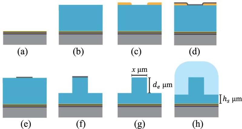
The fabrication and design for the full biosensor can be found in reference [10]. The focus here is in the buried MMI waveguides used in the optimization experiments. To make the buried rib waveguides, we began with a single 100 mm 〈100〉 oriented silicon wafer which had 6 alternating commercially sputtered (Evaporated Coatings Inc.) dielectric films of silicon dioxide (SiO2, n = 1.47) and tantalum pentoxide (Ta2O5, n = 2.107), which form the ARROW layers. The wafer was placed into a PECVD reactor and 6 μm of silicon dioxide (nc = 1.51) was deposited. This film serves as the guiding layer for the excitation, collection and MMI waveguides. The oxide was patterned with positive photoresist (AZ3330) that forms the rib features. A thin film of Ni, ∼100 nm, was then evaporated over the wafer to serve as an etch mask. The Ni covering the resist was removed in a sonicated acetone bath followed by rinsing with isopropyl alcohol (IPA). The sonication ensures smooth side walls and complete removal of Ni in the etch field of the wafer. The rib waveguides were formed by anisotropically etching de μm into the PECVD oxide, using an inductively coupled plasma (ICP) reactive ion etcher (RIE), after which the Ni mask was removed and the waveguides underwent an anneal overnight at 300◦C. Annealing ensures that the oxide is “dry” prior to the cladding layer growth. A 6 μm cladding layer of PECVD SiO2 (n = 1.45) was finally deposited over the rib structures forming buried rib waveguides (BRWs). The same reactor was used for the cladding layer, however the process parameters are adjusted to obtain the lower index of refraction [13].
The lithography mask used for waveguide comparisons consists of different excitation waveguide geometries (x = 2, 4 and 6 μm wide) so comparable structures could be made on the same wafer. The excitation waveguides of various widths couple into 75 μm wide by 1975 μm long MMI waveguides on the same chip for ease of testing and comparison. Different etch depths were achieved by cleaving sections of the wafer after etching a specific depth. The cleaved piece was set aside as the rest of the wafer underwent further etching. This was repeated until various etch depths de were attained.
IV. EXPERIMENTS
To examine which excitation waveguide geometry would produce the optimal input mode, the BRWs with varying excitation widths and depths were characterized by capturing optical mode images for each geometry. Multiple chips with all excitation waveguide widths (measured 2.8 μm, 4.5 μm, 6.5 μm) and specific etch depths were cleaved by diamond scribe to produce smooth facets appropriate for optical testing. Each chip was placed on a chip mount attached to a five axis stage and aligned to a single mode fiber excited by a 633 nm laser (Thorlabs S1FC635). For all tests we coupled light into the fundamental mode of the waveguide. The output mode at the chip edge was guided off-chip by an objective lens and the image captured by a CCD camera. The saved images were then used to calculate the horizontal full-width-at-half-maximum (FWHM) for each mode. Simulations of each expected mode profile for the various geometries were also calculated using Photon Design’s FIMMWAVE software.
In order to characterize the output at the end facet of an MMI waveguide, a figure of merit Peak-Valley Difference (P2VD) is defined as the normalized intensity difference between a detected peak and an adjoining valley, was calculated for each imaged MMI spot pattern. Further, we fit the MMI spot pattern plot into a sum of Gaussian functions using non-linear least square fitting method to obtain the FWHM for each spot in the pattern and took the average. These metrics were used to quantify the fidelity of the MMI waveguide’s interference/spot pattern and verify the input mode is correctly self-imaged. The MMI waveguide output pattern was captured similarly to that of the excitation modes using a white light laser source (NKT Photonics) coupled into the ARROW chip. Wavelength scans between the wavelengths of 430 nm and 670 nm were made to generate different MMI waveguide spot patterns. Those which produced patterns with highest fidelity were recorded. The excitation mode of the MMI waveguides input was then recorded at the wavelengths corresponding to the imaged spot patterns.
To verify that the optimized waveguide geometries improved the overall operation of the optofluidic platform, 200 nm fluorescence beads (FluoSpheresªF8806) stained with Cy-5 and Alexa 488 dyes at a concentration of 107 beads/mL were flowed through the full sensor and excited by the MMI spot pattern at wavelengths of 488 nm, 556 nm and 633 nm to capture fluorescence traces for optimized and non-optimized devices. The setup used to capture the trace is shown in Fig. 1. The fluorescence signal was coupled off chip by a 12 μm wide collection waveguide to a single-photon avalanche photodiode (Excelitas). To eliminate the excitation wavelengths, the signal passed through a single penta-bandpass optical filter (FF01–440/521/607/694/809–25, Semrock).
V. EXPERIMENTAL RESULTS
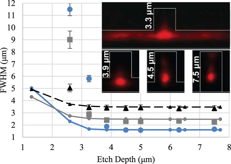
Experimental and simulated results from measuring the FWHM for various excitation waveguides are shown in Fig. 3. Experimental data points come from an average of five waveguides. As expected, narrower excitation waveguides produce tighter optical modes as shown in their FWHM. Also evident is the role that the etch depth plays in the lateral confinement. The FWHM drastically increases at etch depths less than 3 μm for the wider waveguides and 2 μm wide waveguides completely lose confinement at ∼3.5 μm depths. At these depths the experimental data deviates from the simulated data as the rib structures provides little to no confinement for the modes, especially at narrower widths. We attribute this to fabrication refractive index variance in the core and cladding of the BRWs inherent from the deposition method [19] and roughness at the interface from the rib etch. As the etch depth increases, the optical mode becomes more confined and elliptical within the area of the rib itself. Improvement to the mode FWHM stops at around an etch depth of 4 μm. Etching through the oxide into the underlying ARROW layers, an additional ∼1.3 μm, also does not improve the confinement of the mode. These account for the etch depths greater than 6 μm in the graph.
Fig. 3.

FWHM for various width waveguides versus etch depth. (Blue dots = 2.8 μm wide, Gray squares = 4.5 μm wide, Black triangles = 6.5 μm wide, Lines with corresponding shapes and colors are the simulated data of the waveguides with matching widths). Insets ‰âŁ” Mode images captured for 2.8 μm wide waveguides of various etch depths, with rib profiles sketched and rib height de indicated. All data acquired at an excitation wavelength of 633 nm. Experimental error was found to be between 10% and 15% with higher error induced from the multimode nature of the wider waveguides.
As expected, the optimum width to produce tight modes requires waveguides as narrow as lithography conditions allow, here between 2 and 3 μm. The data also indicates that the optimum etch depth for a 6 μm thick SiO2 core layer with a top cladding layer is just over 4 μm. Etching any deeper increases process time and produces excessive etch roughness in the field. Deeper etches tend to form micro pillars in the etch field, which causes the cladding layer to form undesired air pockets as it is deposited over the pillars.
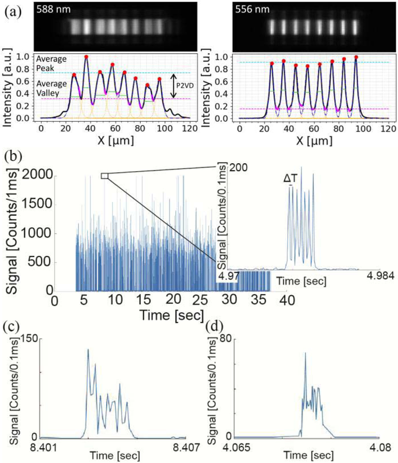
The excitation waveguide for the full optimized optofluidic device used for testing with fluorescent beads, measured to be ∼3 μm wide by 5 μm tall for the optimized device, when imaged by an SEM. Fig. 4a shows MMI pattern taken from top-down view of the liquid core waveguide filled with a quantum dot solution and excited at the wavelength that produced the best 8-spot pattern for each chip. The optimized chip shows improvement in both FWHM and P2VD. In this example, the FWHM drops from 6.3 μm to 4 μm for an optimized device (Quantum dot patterns usually give wider spots than direct facet measurement because of scattering through the top oxide). Likewise, the P2VD increased from 0.42 to 0.75, demonstrating significant performance improvement in both key parameters.
Fig. 4.

Experimental data collected from MMI waveguide with and without optimized geometries. (a) On the left is an MMI waveguide spot pattern taken from un-optimized waveguide, on the right is the pattern for optimized waveguide which shows uniformly distributed spots. Corresponding plots with analysis confirms improvement in both FWHM and P2VD of the spots after optimization. (b) Fluorescence trace acquired from fluorescently labeled 0.2 μm beads flowing through an optofluidic channel excited at 633 nm. The zoomed in trace shows the pattern of the peaks created by an optimized high-fidelity spot pattern. (c-d) The zoomed in bead traces acquired from un-optimized waveguides where (c) is from a 4.8 μm wide excitation waveguide etched 3 μm deep and (d) is from a 5.5 μm wide excitation waveguide etched 4.2 μm deep.
The full optofluidic sensor with optimized waveguide geometries also shows excellent response to the multi-spot MMI excitation. The fluorescence trace shown in Fig. 4b, illustrates data collected at a 633 nm wavelength as beads pass the excitation beams. As we can see, evenly spaced counts are visible when zoomed into the signal. These peaks can be used to identify the passing target because it clearly defines T between peaks. The peaks are quite uniform which will result in improved SNR enhancement after signal processing. Further, the individual spots of the pattern do not produce overlap between spots resulting in reduced background noise and false recognition from the algorithm. The generated peak pattern in Fig. 4b can be compared to peak patterns generated from waveguides that were not optimized in Fig. 4c and d. The non-uniformity of these peaks results in reduced detection accuracy. It is evident that high-fidelity spot patterns produced from MMI waveguides are important for high-sensitivity multiplexed detection of passing target molecules.
Fig. 2.

Buried rib waveguide fabrication process. (a) Begins with ARROW layers deposited on Si substrate (b) Guiding layer oxide deposition (c) Spin on and pattern photoresist (d) Evaporate Ni (e) Ni etch mask shaped from liftoff process (f) Anisotropic etch to form rib structures (g) Remove Ni mask from and anneal rib waveguides of various geometries (h) Deposit cladding layer.
ACKNOWLEDGMENTS
The authors would like to thank T. Yuzvinsky at the W.M. Keck Center for Nanoscale Optofluidics at UC Santa Cruz for assistance with SEM imaging.
This work was supported by NIH under Grant 4R33AI100229 and Grant 1R01AI116989.
Contributor Information
Matthew A. Stott, Department of Electrical and Computer Engineering, Brigham Young University, Provo, UT 84602 USA.
Vahid Ganjalizadeh, School of Engineering, University of California at Santa Cruz, Santa Cruz, CA 95064 USA.
Gopikrishnan Meena, School of Engineering, University of California at Santa Cruz, Santa Cruz, CA 95064 USA.
Johnny McMurray, Department of Electrical and Computer Engineering, Brigham Young University, Provo, UT 84602 USA.
Maclain Olsen, Department of Electrical and Computer Engineering, Brigham Young University, Provo, UT 84602 USA.
Marcos Orfila, Department of Electrical and Computer Engineering, Brigham Young University, Provo, UT 84602 USA.
Holger Schmidt, School of Engineering, University of California at Santa Cruz, Santa Cruz, CA 95064 USA.
Aaron R. Hawkins, Department of Electrical and Computer Engineering, Brigham Young University, Provo, UT 84602 USA.
REFERENCES
- [1].Fan X and White IM, “Optofluidic microsystems for chemical and biological analysis,” Nature Photon, vol. 5, no. 10, pp. 591–597, 2011. [DOI] [PMC free article] [PubMed] [Google Scholar]
- [2].Ozcelik D, Cai H, Leake KD, Hawkins AR, and Schmidt H, “Optofluidic bioanalysis: Fundamentals and applications,” Nanophotonics, vol. 6, no. 4, pp. 647–661, 2017. [DOI] [PMC free article] [PubMed] [Google Scholar]
- [3].CDC. (Jun. 22, 2016). 2014–2016 Ebola Outbreak in West Africa Accessed: Feb. 1, 2018. [Online]. Available: https://www.cdc.gov/vhf/ebola/outbreaks/2014-west-africa
- [4].Osterholm MT, “Ebola and Zika: Cautionary Tales,” Science, vol. 353, no. 6304, p. 1073, 2016. [DOI] [PubMed] [Google Scholar]
- [5].CDC. (2013). Antibiotic Resistance Threats in the United States Accessed: Feb. 1, 2018. [Online]. Available: https://www.cdc.gov/drugresistance/threat-report-2013/pdf/ar-threats-2013-508.pdf
- [6].Ozcelik D et al. , “Optofluidic wavelength division multiplexing for single-virus detection,” Proc. Nat. Acad. Sci. USA, vol. 112, no. 42, pp. 12933–12937, 2015. [DOI] [PMC free article] [PubMed] [Google Scholar]
- [7].Ozcelik D et al. , “Signal-to-noise enhancement in optical detection of single viruses with multispot excitation,” IEEE J. Sel. Topics Quantum Electron, vol. 22, no. 4, Jul-Aug 2016, Art. no. 4402406. [DOI] [PMC free article] [PubMed] [Google Scholar]
- [8].Lien V, Zhao K, Berdichevsky Y, and Lo Y-H, “High-sensitivity cytometric detection using fluidic-photonic integrated circuits with array waveguides,” IEEE J. Sel. Topics Quantum Electron, vol. 11, no. 4, pp. 827–834, Jul. 2005. [Google Scholar]
- [9].Parks JW, Wall TA, Cai H, Hawkins AR, and Schmidt H, “Enhancement of ARROW photonic device performance via thermal annealing of PECVD-based SiO2 waveguides,” IEEE J. Sel. Topics Quantum Electron, vol. 22, no. 6, pp. 249–254, Nov-Dec 2016. [DOI] [PMC free article] [PubMed] [Google Scholar]
- [10].Wall T, McMurray J, Meena G, Ganjalizadeh V, Schmidt H, and Hawkins AR, “Optofluidic lab-on-a-chip fluorescence sensor using integrated buried ARROW (bARROW) waveguides,” Micromachines, vol. 8, no. 8, p. 252, 2017. [DOI] [PMC free article] [PubMed] [Google Scholar]
- [11].Cai H, Stott MA, Ozcelik D, Parks JW, Hawkins AR, and Schmidt H, “On-chip wavelength multiplexed detection of cancer DNA biomarkers in blood,” Biomicrofluidics, vol. 10, p. 064116, Dec. 2016. [DOI] [PMC free article] [PubMed] [Google Scholar]
- [12].Ozcelik D et al. , “Scalable spatial-spectral multiplexing of single-virus detection using multimode interference waveguides,” Sci. Rep, vol. 7, Sep. 2017, Art. no. 12199. [DOI] [PMC free article] [PubMed] [Google Scholar]
- [13].Wall T et al. , “Mitigating water absorption in waveguides made from unannealed PECVD SiO2,” IEEE Photon. Technol. Lett, vol. 29, no. 10, pp. 806–809, May 15, 2017. [DOI] [PMC free article] [PubMed] [Google Scholar]
- [14].Soldano LB and Pennings ECM, “Optical multi-mode interference devices based on self-imaging: Principles and applications,” J. Lightw. Technol, vol. 13, no. 4, pp. 615–627, Apr. 1995. [Google Scholar]
- [15].Ulrich R and Kamiya T, “Resolution of self-images in planar optical waveguides,” J. Opt. Soc. Amer, vol. 68, no. 5, pp. 583–592, 1978. [Google Scholar]
- [16].Chung L-W, Lee S-L, and Lin Y-J, “Principles and application of reduced beat length in MMI couplers,” Opt. Express, vol. 14, no. 19, pp. 8753–8764, 2006. [DOI] [PubMed] [Google Scholar]
- [17].Besse PA, Bachmann M, Melchior H, Soldano LB, and Smit MK, “Optical bandwidth and fabrication tolerances of multimode interference couplers,” J. Lightw. Technol, vol. 12, no. 6, pp. 1004–1009, Jun. 1994. [Google Scholar]
- [18].Vázquezl C, Tapetado A, Orcutt J, Meng HC, and Ram R, “Tolerance analysis for efficient MMI devices in silicon photonics,” Proc. SPIE, vol. 8990, p. 89900A, Mar. 2014. [Google Scholar]
- [19].Zhou H, Kim HK, Shi FG, Zhao B, and Yota J, “Optical properties of PECVD dielectric thin films: Thickness and deposition method dependence,” Microelectron. J, vol. 33, no. 11, pp. 999–1004, 2002. [Google Scholar]


