

Abstract
Objective:
To improve the existing manually-assembled cochlear implant electrode arrays, a thin film electrode array (TFEA) was micro-fabricated to have a maximum electrode density of 15 sites along an 8-mm length, with each site having a 75 × 1.8-μm (diameter × height) disk electrode.
Methods:
The micro-fabrication method adopted a sequence of photoresist transferring, lift-off, two-step oxygen plasma etching, and fuming nitric acid release to reduce lift-off complexity, protect the metal layer, and increase the release efficiency.
Results:
Systematic in vitro characterization showed that the TFEA’s bending stiffness was 6.40 × 10⁻¹⁰ N·m2 near the base and 1.26 × 10⁻¹⁰ N·m2 near the apex. On average, the TFEA electrode produced an impedance of 16 kΩ and a maximum current limit of 800 μA, measured with a 1-kHz sinusoidal current using monopolar stimulation in saline. A TFEA prototype was implanted in a cat cochlea to obtain in vivo measurements of electrically-evoked auditory brainstem and inferior colliculus responses to monopolar stimulation with 41-μs/phase, biphasic pulses. Both physiological responses produced a threshold of ~300 μA and a dynamic range of 5–8 dB above the threshold. Comparing with existing electrode arrays, the present TFEA had 104 times less bending stiffness, 97% less electrode area, and comparable physiological thresholds.
Conclusion:
Using a simplified structure and stable fabrication method, the present TEFA produced physical and physiological performance comparable to existing commercial devices.
Significance:
The present TFEA and micro-fabrication method represent a step closer towards an automated process replacing the labor-intensive and expensive manual assembly of electrode arrays in most neural prostheses including the cochlear implant.
Keywords: Cochlear implant, MEMS, Parylene, Thin film electrode array, Electrode impedance, Auditory brainstem responses, Inferior colliculus, Threshold, Dynamic range
I. Introduction
The cochlear implant (CI) has been one of the most successful neural prostheses to date. At present, commercially available cochlear implant electrode arrays are all manually assembled, consisting of a wire-bundle design with 12–26 electrodes, a length of 16–30 mm, an electrode interval of 0.75–2.4 mm, and an electrode surface area of 0.12–1.5 mm2 [1]. These fundamental design features have not changed in the last 30 years, despite advances that have been made in signal processing, biomaterials, and semiconductor fabrication. As a result, the performance and accessibility of CIs have been limited by the relatively small number of electrodes and labor-intensive assembly of the electrode array [2] [3].
Micro-fabrication may improve the existing commercial products for it not only enables integrated micro-scale electrodes and interconnecting wires, but also lowers the manufacturing cost by scalability. Thin-film electrode arrays (TFEAs) have been used in various applications, including retinal and spinal cord prosthetics, and electromyographic signal recordings [4] [5] [6]. For CIs, TFEAs have been developed from boron diffusion silicon (Si) substrate designs [7] [8] to flexible polymer substrate designs [9]. The state-of-the-art cochlear TFEA developed by Johnson and Wise contains 32 electrodes on an 8-mm-long array in a curve-controlled shape with a system-level ASIC [10]. Despite these significant advances [11] [12], none of the MEMS electrodes is currently used in commercial CIs applications for humans. A TFEA with lower risk of structural delamination and less complexity of fabrication is still needed for actual cochlear implant application, especially over a long period of time that is comparable to the current commercially available manually-assembled cochlear implant arrays.
Here a Parylene TFEA was developed for cochlear implants. An improved fabrication process reduced the lift-off complexity while increasing both the metal layer protection and the release efficiency. Section II details the design and fabrication. Section III systematically characterizes the fabricated TFEA in vitro to measure its mechanical and electrical properties. Section IV systematically characterizes the array in vivo in a cat model to measure its physiological responses. Section V compares both physical and physiological performance of the present TFEA, commercial arrays, and other TFEAs. Section VI shows that the present TFEA significantly simplifies the structure and the fabrication process while producing comparable performance.
II. Design and Fabrication
A. Materials
Parylene C, a thermoplastic semicrystalline polymer, was chosen as the substrate and encapsulation layer for the TFEA because of the following favorable properties. First, Parylene C has a Young’s modulus of ~3.2 GPa, which is much more flexible than rigid Si (130–188 GPa). Second, Parylene C has a dielectric constant of 3.1 F/m at 1 kHz [13], which provides sufficient electrical insulation [4]. Third, Parylene C is mostly immune to hydrolytic degradation, enabling long-term usage in the cochlear perilymph. Fourth, Parylene C is biocompatible, which is evidenced by the United States Food and Drug Administration’s approval of Parylene-coated devices.
Platinum (Pt) was chosen as the electrode material. As one of the most popular bio-potential electrode materials, Pt exhibits well-documented biocompatibility and electrochemical stability [1]. Furthermore, Pt has a charge density limit of 0.4 mC/cm2, which is greater than the safe stimulation charge density for auditory neurons (0.15 mC/cm2) [14]. Titanium (Ti) was chosen for its strong adhesion to Parylene C [15].
B. Design
The design parameters and schematics are shown in Table I and Fig. 1, respectively. Two versions of the TFEA were designed. Both versions contained disk electrodes, which had a three-dimensional (3D) convex profile and a diameter of 150 μm. The annular area near the rim, approximately 75 μm in width, was covered by the Parylene C insulating layer. The apical end of the TFEA had a “round” top for easy insertion. The basal end of the TFEA contained terminal pads for electrical connections.
Table I.
Design parameters for the TFEA
| Design parameter | Long TFEA | Short TFEA |
|---|---|---|
| Length | 16 mm | 8 mm |
| Apical width | 0.7 mm | 0.5 mm |
| Basal width | 1.2 mm | 1 mm |
| Exposed electrode diameter | 75 μm | 75 μm |
| Electrode interval | 200 μm (minimum) | 200 μm (minimum) |
| Minimum wire width | 15 μm | 15 μm |
| Minimum wire spacing | 13 μm | 13 μm |
| Total thickness | 7.8 μm | 7.8 μm |
| Substrate thickness | 5 μm | 5 μm |
| Maximum electrode density | 23 sites/16 mm | 15 sites/8 mm |
Fig. 1.

Design schematics of the cochlear TFEA. (a) Schematic of the TFEA inserted into the scala tympani along the lateral wall. (b) Top view of a TFEA, (c) enlarged top view, and (d) cross-sectional view of the electrode site.
C. Fabrication
From Fig. 2, 500-nm aluminum (Al) was first evaporated as the sacrificial layer. 2.2-μm positive photoresist AZ GXR-601 was spun and patterned as the electrode mold. Then 5-μm Parylene C was deposited at ~1.84 g/μm as the substrate of the TFEA (PDS2010 Specialty Coating System, Indianapolis, IN, USA). 20-nm Ti and 200-nm Pt were patterned by lift-off using NR9–3000PY negative photoresist as the electrodes and wires. After cleaning the Parylene substrate with O2 plasma, 1-μm Parylene was deposited as the insulation layer. To pattern the Parylene, a two-step etching process was conducted: 2.2-μm positive photoresist AZ GXR-601 was first patterned to define the electrodes, and the exposed insulation layer was etched with reactive ion O2 plasma etching (O2 RIE etching) (Branson IPC 3000, SemiStar Corp., Morgan Hill, CA, USA) to expose the electrodes. 13.5-μm positive photoresist AZ4620 were then patterned to define the profile of TFEA, followed by an inductively coupled O2 plasma etching process (O2 ICP etching) (NE 550, ULVAC Technologies, Inc., Methuen, MA, USA) to etch the Parylene C outside the TFEA. The wafer was then immersed into fuming nitric acid to remove the residual photoresist and release the TFEA. The released TFEA was cleaned, dried, and vacuum annealed at 150 °C for 12 h, which strengthened the adhesion between the Parylene layers. To mechanically enhance the TFEA and avoid buckling during insertion, a pre-shaped polyimide tape carved by a fine scalpel was adhered to the back of the TFEA. The TFEA was then connected to the PCB board with pre-aligned spring-loaded pins (pogo pins).
Fig. 2.

Schematics of fabrication process
D. Results
A total of 97 TFEAs were fabricated on one 4-inch wafer with a yield rate of ~71%. The yield loss was mainly due to the residual stress that twisted the TFEA after release. Fig. 3 (a) and (b) show the 8-mm and 16-mm TFEA samples, respectively; (c) and (d) show the circular electrode area with the center (75 μm diameter) being exposed and other areas, including the interconnecting wires, being covered by the Parylene insulation layer; (e) and (f) show the 3D convex disk electrode, with the electrode surface 1.8 μm being higher than the top surface of the Parylene insulation layer (measured by the S neox non-contact 3D surface profiler, Sensofar, Barcelona, Spain).
Fig. 3.
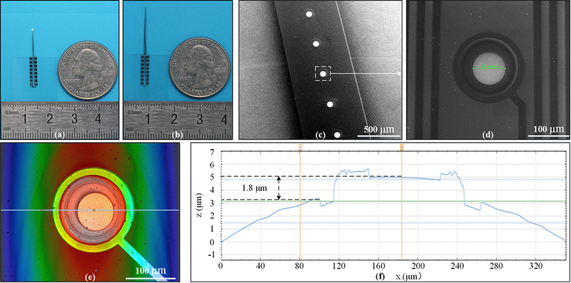
Fabrication results of the TFEA. Optical images of an 8-mm-long TFEA (a) and a 16-mm-long TFEA (b). SEM images of the TFEA with 500-μm (c) and 100-μm (d) magnifications. (e) A 3D profile of the TFEA electrode site. (f) Profile plotted with the data along the horizontal blue line in (e).
E. Discussion
The present design and fabrication process led to the following improved features. First, the convex profile of the AZ GXR-601 photoresist was transferred to the metal layer above it, which was a result of the favorable conformality of Parylene coating. As shown in Fig. 4, because AZ GXR-601 exhibited higher light absorptivity at the top surface compared with the bottom surface, the underlying AZ GXR-601 formed a trapezoid structure after lithography, which produced a smooth slope at the electrode edge to ensure the sputtered metal continuity. Secondly, the lift-off process led to a minimum wire spacing and wire width of 12.6 μm and 15.6 μm, respectively. Compared with previous attempts utilizing double-layer photoresist or the TMAH surface hardening technique [10] [16], the procedures were simplified with negative photoresist.
Fig. 4.

(a) Schematic of trapezoid structure of AZ GXR-601 resulted from the light absorptivity difference during the lithography. (b) SEM image of the electrode area. Inset: zoom-in image showing the trapezoid slope at the edge of electrode.
Fig. 5 compares the previous single etching process (a) with the present two-step process (b) and their control experiment results (c) (d). The first step in the present process used O2 RIE etching to expose the electrodes and terminal pads while the second step used O2 ICP etching to define the profile of TFEA. Some ICP machines, before finishing the etching process, require an Argon (Ar) de-chuck step that can physically collide with the electrode surface. The present two-step process thus had the following two benefits. (1) Reduced damage to the electrode surface when Ar is employed during the etching process. (2) Less etching depth in the first etching step enabled better control of the sizes of exposed electrodes considering the notable lateral etching depth (O2 RIE aspect ratio: 5:1).
Fig. 5.

(a) Schematic of the traditional single step ICP process. (b) Schematic of the two-step etching process applied in this work (all colors correspond with those in Fig. 2). Optical microscope images: (c) Pt layer damage after the single-step ICP process. (d) Pt in good condition after the two-step etching process.
In the previous works, Parylene devices were released with photoresist as the sacrificial layer and acetone as the solvent [4], or Al as the sacrificial layer and Al etchant as the solvent [17], or peeling off the device from the Si wafer directly [5]. Adopting photoresist as the sacrificial layer limits the process compatibility because photoresist is soluble in many solvents. Also, the reaction rate of Al in the Al etchant (H3PO4: HAc: HNO3 = 16:2:1) is slow (530 nm/min) [18]. In addition, peeling off the device directly may rip the device because of its flimsy structure and low tensile strength. The present approach used Al as a sacrificial layer to guarantee the process compatibility. Fuming nitric acid was chosen as the etchant for three reasons: (1) to remove photoresist, especially after plasma etching; (2) to etch Al, creating space beneath the TFEA; and (3) to utilize its high volatility, boosting the solvent’s micro-motion and helping release the TFEA without entirely etching the sacrificial layer. With the present method, all TFEAs were successfully released from the wafer in 20 minutes with no residual photoresist.
III. In vitro characterizations
A. Mechanical bending experiment
Fig. 6 (a) shows the experimental protocol to evaluate the bending stiffness of TFEA. A force sensor probe (FT-S Microforce Sensing Probe, FemtoTools AG, Buchs, Switzerland) with a precision of 0.005 μN was vertically mounted onto a micromanipulator. An 8-mm TFEA was horizontally attached to a stable platform, with a fixation position being set at either electrode #15 (near the basal end towards the platform) or electrode #3 (near apical position close to the tip of the array). A bending force was applied 1 mm away from the fixation position in the direction normal to the surface of the TFEA. Fig. 6 (b) shows that the measured force increased linearly as a function of the bending displacement within the elastic deflection range. The TFEA was approximately modeled as a cantilever beam with a rectangular cross-section [19]. With (1), the bending stiffness (EIz) of the basal and apical part was calculated to be 6.40 × 10⁻¹⁰ N·m2 and 1.26 × 10⁻¹⁰ N·m2, respectively.
Fig. 6.

(a) Schematic of the bending experiment. (b) Force-displacement function for the bending experiment of an 8-mm TFEA. Apical and basal bending lengths were both 1 mm.
| (1) |
B. Electrical characterization experiment
The cochlear implant-electrode interface can be analyzed in an equivalent circuit model [20] with lumped parameters, as depicted in Fig. 7. Stimulating current flows through the scala tympani, which is represented by a resistive network, and returns to the ground to produce an intracochlear electric field and a neuron activation pattern [21]. At the electrode-perilymph interface, the Warburg resistance RW and capacitance CW are used to model the capacitive effects of the double layer of metal and perilymph. In parallel to RW and CW is the Faradic resistance RF, modeling the electron charge transfer across the interface. In addition, RB is the bulk resistance associated with the nearby electrode solution resistance [22] [23]. The proposed TFEA was herein characterized in the following three experiments.
Fig. 7.

Equivalent circuit of the electrode-cochlea system. Axoplasmic resistance network: axoplasmic resistance Rn. Perilymph-spiral lamina interface: membrane capacity Cm, membrane resistance Rm. Cochlear perilymph resistance network: perilymph resistance RL, RT. Electrode-perilymph interface: Warburg capacitance CW, charge transfer resistance RF, bulk resistance RB.
1). Electrical impedance spectroscopy (EIS)
In the EIS experiment, the impedance spectrum of the electrode-electrolyte system was obtained by an electrochemical workstation (PGSTAT 302F, Metrohm AG, Herisau, Switzerland) from 1 Hz to 100 kHz. As shown in Fig. 8 (a), the EIS experiment was conducted with an 8-mm/15-site TFEA in the 0.01 mol/L phosphate buffer saline (1×PBS). A three-electrode system was deployed with a TFEA electrode as the working electrode, an Ag/AgCl electrode as the reference electrode, and a Pt electrode as the counter electrode. Fig. 8 (b) shows the magnitude and phase spectra, which demonstrates that the TFEA’s electrode had an average impedance magnitude of 15.8 kΩ at 1 kHz. The impedance phase angle ranged from −72.8° to −14.8°, indicating that the electrode impedance contained both resistive and capacitive components in the frequency range.
Fig. 8.

EIS Experiment: (a) schematic and (b) frequency-dependent impedance spectrum. The data were measured from 4 electrodes with the error bar representing the mean and standard deviation.
2). Biomimetic stimulation experiment
An in vitro stimulation experiment was conducted to mimic the CI environment. An 8-mm TFEA was inserted into a quartz tube (diameter: 4.5 mm) in the 0.01 mol/L phosphate buffer saline (1× PBS) to simulate scala tympani and cochlear perilymph, as shown in Fig. 9 (a) and (b). Unlike a voltage source used in the electrical impedance spectroscopy experiment, a constant current source was used to deliver electric stimulation continuously for one minute. The electric potential across the current source was recorded with a digital oscilloscope. Two electrode configurations were employed: The monopolar mode (MP) used an electrode from the TFEA as the stimulating electrode and a large tinning plate copper wire as the ground electrode. The bipolar mode (BP) used two electrodes from the TFEA as the stimulating electrode and the ground electrode, respectively. Here the BP+1 mode was evaluated, in which electrode #n served as a stimulating electrode and #(n+1) as the ground electrode.
Fig. 9.

Biomimetic electrical experiment. (a) Schematic including MP stimulation, BP stimulation, and electric field imaging (EFI). (b) TFEA immersed in a quartz tube in the PBS. (c) Two channels employed during the experiment with sinusoidal current: Channel 1 recorded the electric potential across the current pathway and Channel 2 recorded the EFI electric potential. (d) Impedance measurements of TFEA electrodes in MP mode and BP mode. The data were measured from one 8-mm TFEA’s 15 electrodes. For each electrode, the measurement lasted for 1 minute, which led to ~600 measurements. For each 1-minute measurement, the error bar represents the maximum and the minimum electrode impedance. The data point represents the median value. (e) Stimulation of biphasic pulses: Channel 1 recorded the electric potential across the current pathway and Channel 2 recorded the electric potential across the 1-k resistor. (f) Current level-dependent impedance results. The data were measured from one 8-mm TFEA’s electrode #1, stimulated with different current level. For each current level, the measurement lasted for 1 minute, which led to ~600 measurements. For each 1-minute measurement, the error bar represents the maximum and the minimum electrode impedance. The data point represents the median value.
Using 1-kHz 100-μA sinusoidal current as the input, the impedance of the TFEA electrodes were characterized as a function of electrode number in both the MP and BP modes, as shown in Fig. 9 (d). The MP impedance was relatively uniform across all 15 electrodes, with an average of 11.2 (±0.7) kΩ. This average value was 30% lower than the electrical impedance spectroscopy result of 15.8 kΩ, probably due to the much longer 1-min stimulation duration used in the biomimetic experiment [24]. In contrast, the BP+1 mode produced an average impedance of 23.2 (±1.1) kΩ, doubling the MP impedance approximately, a rise as expected [25]. In addition, the BP mode was used to detect short-circuit failures between electrodes. No short-circuit failures were found in the present experiment.
Impedance was also measured for charge-balanced biphasic pulses, the most commonly used stimulation waveform in contemporary cochlear implants. In response to a 500-μA constant current biphasic pulse, the potential pattern showed a “charge-discharge” characteristic, illustrated in Fig. 9 (e) channel 1. The estimated impedance ranged from 10.1 to 10.6 kΩ for 30-μs/phase biphasic pulses, and from 10.4 to 10.7 for 50-μs/phase biphasic pulses. To ensure charge balance, a 1-kΩ series resistor was added to the current pathway. A symmetrical charge-balanced potential waveform was found across the 1-kΩ resistor, as shown in Fig. 9 (e) channel 2.
To find the maximum current limit, 1-kHz sinusoidal current was applied to TFEA electrode #1 in the MP mode. Fig. 9 (f) shows that the impedance decreased as a function of current level from 20 to 700 μA. When the current level reached 800 μA, the impedance became infinite, indicating an open circuit due to irreversible electrode damage. With a 1-kHz, 50 μs/phase biphasic pulse train, the maximum current level was 900 μA.
3). Electric field imaging
The TFEA may be used for electric field imaging (EFI), in which one electrode serves as a stimulating site whereas all other electrodes are used to record electric field potentials [26]. Fig. 10 shows the electric field imaging results in response to a 16-mm TFEA’s stimulating electrode #1 (a), #8 (b), and #15 (c), respectively. The stimulus was a 1-kHz, 100-μA sinusoidal current delivered in the MP mode. The electric potential decreased monotonically as a function of the distance between the recording and the stimulating electrodes [20]. Fig. 11 (red symbols and lines) also shows the electric field imaging result in response to a 1-kHz 50-μA sinusoidal current from a HiFocus electrode array (Advanced Bionics, Valencia, CA, USA) in human subjects [27]. The human data were generally within 1 and 2 times of the present data. The <2x difference was actually small, considering the significant differences between the human cochlea and the present quartz tube.
Fig. 10.

Electric field imaging results: (a) stimulating with electrode #1, (b) stimulating with electrode #8, and (c) stimulating with electrode #15. The data were measured from one 16-mm TFEA’s other 14 recording electrodes. For each recording electrode, the measurement lasted for 1 minute, which led to ~600 measurements. For each 1-minute measurement, the error bar represents the maximum and the minimum electric potential. The data point represents the median value. The blue symbols and lines represent data from the present 16-mm 15-sites TFEA whereas the red symbols and lines are from the HiFocus electrode array. The distance between two adjacent electrodes is 1.1 mm for both electrode arrays.
Fig. 11.

(a) TFEA insertion in the cat model. (b) Auditory nerve activity recorded from eABRs in response to TFEA stimulation using 41 μs/phase biphasic pulses. (c) STC elicited by the electric stimulation delivered to TFEA electrode #1 and #3.
IV. In vivo characterizations
To assess the TFEA’s insertion into the cochlea and feasibility in eliciting neural responses, an in vivo experiment was conducted in an anesthetized cat model. The experiment followed the same protocol as described previously [28] [29]. The protocol was in accordance with National Institutes of Health Guidelines (Guide for the Care and Use of Laboratory Animals, 1996) and had been approved by the Institutional Animal Care and Use Committee at the University of California, Irvine.
A 32-site silicon-substrate recording probe (NeuroNexus Technologies, Ann Arbor, MI, USA) was implanted into the right central nucleus of the inferior colliculus (ICC) with a micromanipulator. Prior to deafening the ear and insertion of the TFEA, pure-tone sound stimuli were presented at a range of frequencies and levels to determine characteristic frequencies (CFs) of neurons. The position of the ICC recording probe was adjusted to sample a range of CFs from 1 Hz to 32 kHz. After final determination of the CF at each of the 32 recording sites was made, the recording probe was fixed with agarose, wax, and dental acrylic, and was released from the micro-positioner. The cat was repositioned to allow access to the left cochlea contralateral to the recording site of ICC. Following full exposure of the round window of the left cochlea, a drill was used to augment the round window opening into the basal turn of the cochlea, and the round window membrane was removed. Neomycin sulfate (10 % in water) was injected into the cochlea to deafen the ear [28]. After connecting the TFEA device with the stimulator, a 16-mm 15-site TFEA was gently inserted approximately 7 mm into the left cochlea with a micromanipulator, along with a gold electrode in the skin behind the stimulated ear as the return electrode for the stimulation. Conventional sub-dermal electrodes were used to record electrically evoked auditory brainstem responses (eABR).
Monopolar stimulation with a 10-Hz cathodic-first 41 μs/phase biphasic pulse train was delivered to derive physiological responses. System 3 equipment (TDT; Alachua, FL, USA) was employed for stimulus presentation and data acquisition with a customized program running in MATLAB (The MathWorks, Natick, MA, USA).
Fig. 11 (b) shows recorded eABR waveforms as a function of electric stimulation delivered to electrode #3, which was 4.5 mm away from the apical end of the TFEA. The first biphasic peaks with unchanged latency close to 1 ms represented electric stimulation artifact. Starting at 316 μA, electric stimulation elicited robust neural responses as evidenced by systematically increased peak amplitude and shortened peak latency of eABR wave I to V. The level of 316 μA was defined as the threshold, whereas the measured dynamic range was 8 dB ( = 20log(794 μA/316 μA)).
Fig. 11 (c) shows recorded spatial tuning curves (STC) in response to electrical stimulation from electrode #1 and #3, which indicated ICC activity along the tonotopic axis as a function of stimulus level. The contours represented the cumulative discrimination index (cumulative d’) for the discrimination of changes in trial-by-trial spike count at single ICC recording sites, induced by a successive 1- to 2-dB increase in current level (the definition of d’ was detailed in Appendix). The contours were drawn in steps of one d’ unit (i.e., ten steps in the colorbar, from d’ = 1 to 10, d’ = 1 represented the threshold) [29], and illustrated the range of ICC depths at which electric stimulation produced suprathreshold neural activities with a criterion of d’≥1. The neural threshold (red circle) was ~270 μA for both electrodes. The measured dynamic range was 5 dB ( = 20log(501 μA/270 μA)). For electrode #1 and #3, the 3-dB STC width (the contour width at the current level 3 dB above the threshold) was >600 μm and >850 m, respectively. The most sensitive frequency (red dash line) was ~30 kHz in response to electrode #1 stimulation and ~32 kHz to electrode #3 stimulation, corresponding to the more apical location of electrode #1 over that of electrode #3.
V. Discussion
A. Comparison of fabrication methods
Compared with the traditional manual assembly method, the present micro-fabrication method can be batch processed with potentially a high volume and a low cost. The minimum wire width was 15.6 μm, which was 62% of the size of commercial cochlear implant electrode arrays’ Pt-Ir alloy (diameter: 25 μm, Nucleus 22 [30]). The maximum electrode density of the proposed TFEA was 15 sites/8 mm, which was 36% higher than contemporary arrays (the maximum electrode density reported to date was 24 sites/20 mm, Nurotron Venus electrode array [31]). Table II directly compares the fabrication methods between the present TFEA and the state-of-the-art design by Johnson and Wise [10]. The present TFEA method had the following 5 advantages. (1) Although the number of lithography steps is the same, the first and third lithography steps in the present method did not require the removal of photoresist. In addition, the first lithography step was optional and was only required when a 3D electrode was needed. (2) The present method required one less metal deposition process. (3) The present lift-off did not require pre-treatment of the photoresist and used sputtered metal, which simplified the lift-off steps and improved adhesion to Parylene. The final soaking time in the photoresist removal was reduced from 5 hours to 40 minutes. (4) One less layer of Parylene reduced the possibility of Parylene delamination. (5) The release efficiency was improved as the whole release process could be finished in 20 minutes, compared with the time of etching the whole wafer with 2% KOH.
Table II.
comparison of the present TFEA with Johnson and Wise’s TFEA
| The present TFEA | Johnson and Wise’s electrode array | |
|---|---|---|
| Lithography | 4 lithography processes: | 4 lithography processes: |
| 1 for the 3D electrode formation (Optional) | ||
| 1 for metal wires patterning. | ||
| 1 for the metal layer patterning. | ||
| 1 for the electrode sites patterning | ||
| 2 for the two-step Parylene etching (The 1st and 3rd lithography do not require photoresist removal.) | ||
| 2 for the Parylene etching. | ||
| Metal deposition | 1 sputtering | 1 evaporation and 1 sputtering |
| Lift-off | NR9 3000PY as the photoresist. | AZ9260 as the photoresist. |
| TMAH surface-hardening technique. | ||
| Sputtered metal (Ti 20 nm, Pt 200 nm). | ||
| Evaporated metal wires (Cr 20nm, Au 300nm, Cr 20nm). | ||
| RR41 soaking for 40 minutes to lift off. | ||
| Acetone soaking for 5 hours to lift off. | ||
| Parylene deposition | 2 | 3 |
| Electrode protection | Two-step O2 plasma etching. | Sputtering parameters optimized from experience (Base pressure: 2 nTorr or less; power: 300W; sputter pressure: 8.5 mTorr). |
| Release | Al-Fuming nitric acid released in 20 mins. | Etching the whole wafer with 2% KOH. |
B. Comparison of technical parameters
Mechanically, the Nucleus straight/Contour arrays (Cochlear Ltd., Sydney, Australia) have basal and apical bending stiffness of 9.85 × 10⁻⁶ N·m2/1.47 × 10−6 N·m2 and 7.84 × 10⁻⁶ N·m2/5.58 × 10−7·N·m2, respectively [37]. In contrast, the present TFEA had 104 times less bending stiffness. While a less stiff array may contribute to less trauma during implantation, too much flexibility increases the difficulty in surgical insertion. One way to increase stiffness is to apply a TFEA carrier as the present TFEA to avoid buckling in surgical insertion, which made the present TFEA 103 times stiffer according to our measurement. Another way is to add reinforcing structures including rings or ribs to the back of TFEA, which leads to a 41% increase of bending stiffness [10].
Fig. 12 (a) compares electrode impedance between the present TFEA and existing arrays. On average, the electrode impedance of the present TFEA (16 kΩ measured in electrical impedance spectroscopy) was 160% and 17% of that of the commercial arrays (10 kΩ) and other TFEAs (90 kΩ), respectively. Fig. 12 (b) shows that the electrode diameter of the present TFEA work was 17% and 42% of that of the commercial arrays (450 μm on average) and other TFEAs (180 μm), respectively. As a tightly controlled study, the TFEA from Jonathan et al. was investigated with the same experimental setup (Electrical impedance spectroscopy in 1×PBS, 1 kHz) as our TFEA. Their electrode area and impedance are 16% lower and 21% higher than the TFEA in this work, respectively. Except for the two-step O2 etching process that protected the electrode, the electrode impedance of the TFEA was further reduced by the O2 plasma cleaning process before the deposition of Pt, which created 3D microstructures and increased the real electrode surface area. Further electrochemical experiments will help analyze the mechanism between the impedance and design parameters.
Fig. 12.

Comparisons between the TFEA and other commercial counterparts: (a) impedance comparison and (b) electrode diameter comparison. Note: All the electrode arrays use Pt as the electrode material. Measuring conditions: the present TFEA: 50 μs/phase, 1-kHz monopolar sinusoidal current, PBS, 1 minute. Nucleus 24M double electrode array: 25 μs/phase, 250-Hz biphasic pulses, human subjects, measured when switching on the device [32]. Combi 40+ electrode array: 26.7 μs/phase, 250-Hz biphasic pulses, human subjects, measured when switching on the device [33]. Clarion CI HiFocus/Helix electrode array: 1-kHz sinusoidal current, human subjects, measured when switching on the device [24]. Nurotron Venus electrode array: 40 μs/phase, 1-kHz biphasic pulses, human subjects, measured when switching on the device [34]. NeuroNexus Technology probe: 1-kHz sinusoidal current, PBS [35]. Jonathan et al.’s TFEA: 1 kHz, EIS measurement in PBS [36] Other data source for the electrode diameter: Cochlear Ltd. reference guide-electrode comparison. MED-EL electrode arrays for professionals.
The present TFEA had a maximum biphasic pulse current level of 900 μA. Shannon’s charge density model was employed to predict the maximum current level for the TFEA electrode [38]:
| (2) |
where I is the safety limit of current level, T is the phase duration, and k is chosen as 1.5 as the safety limit. Using a 75-μm-diameter TFEA electrode and 50-μs/phase biphasic pulses in the model, a theoretical safe current level of 747 μA was obtained. At 900 μA, which was recorded in the biomimetic experiment, the electrode was damaged by hydrolysis reactions. Enlarging the exposed electrodes can expand the dynamic range of TFEA without sacrificing the electrode density. In particular, the safe current level of the TFEA can be increased to 1.12 mA by increasing the exposed electrode diameter by 50%, which is still scalable based on the present fabrication design and results.
Fig. 13 compares physiological responses between the present and previous devices. In the in vivo experiment, the eABR threshold was 316 μA with 41- μs/phase biphasic pulses, corresponding to a charge of 13.0 nC. In comparison, the Nucleus 22M electrode array (Cochlear Ltd., Sydney, Australia) and the TFEA from Johnson and Wise have a threshold charge of 14.8–37.8 nC [39] and 10.0 nC [10], respectively. The present TFEA produced a similar eABR threshold charge, as shown in Fig. 13 (a).
Fig. 13.

Comparisons of the in vivo results: (a) eABR threshold charge, and (b) ICC threshold.
Fig. 13 (b) compares the ICC thresholds between the present and previous devices. In the in vivo experiment, the ICC threshold was 276 μA with a 41-μs/phase single biphasic pulse. The present TFEA’s ICC threshold was between the threshold of the Nucleus 22M array (340 μA) and the intraneural stimulating array (NeuroNexus Technologies, Inc., Ann Arbor, MI, USA) (20.4 μA) employed by Middlebrooks and Snyder with similar experimental protocols [29], likely reflecting the different distance between the electrode and cochlear nerves.
VI. Conclusions
To break the barriers of low resolution and high cost of manually assembled cochlear implant electrode arrays, a micro-fabricated Parylene thin film electrode array was developed and evaluated with the following results: (1) 1.8-μm high, 75-μm diameter disk electrodes fabricated by a photoresist transferring process, (2) an electrode density of 15 sites on an 8 mm length, realized by a simplified 15-μm-resolution lift-off process, (3) improved metal quality by a two-step Parylene C etching process, and (4) increased release efficiency by using aluminum as the sacrificial layer and fuming nitric acid as the etchant. Comparing with previously reported thin-film arrays, the present design has a simpler structure and more stable fabrication method. Systematic in-vitro and in-vivo evaluation showed that the present design had ~104 times less bending stiffness, 97% less electrode area, but similar physiological thresholds and responses compared with contemporary cochlear implant electrode arrays. The present study suggests that micro-fabrication is a feasible method to replace the labor-intensive and expensive process of manufacturing electrode arrays in cochlear implants and other neural prostheses.
Acknowledgment
The authors would like to thank Professor Wei Wang from Peking University, Dr. Kaichen Dong from Tsinghua University, Dr. Phillip Tran, Dr. Alessandro Presacco, M.D. Hamid Djalilian from University of California, Irvine for their helpful comments. The authors would like to thank Tsinghua Nanofabrication technology center and Zibo Hi-tech industrial development zone MEMS research institute for providing the fabrication platform for this work. The authors would also like to thank Tsinghua University for providing the overseas study scholarship.
This work was funded by National Nature Science Foundation of China (5405260), Beijing Laboratory for Biomedical Detection Technology and Instrument, and Center for Hearing Research, University of California Irvine.
Footnotes
Appendix
IC responses were demonstrated in the STC plots, in which the colored contours represented the value of cumulative discrimination index (d’), linking to the stimulus-driven growth of response at each of the ICC recording sites. d’ is the neural response discrimination of electrical stimulus levels differing by 1–2 dB. Based on responses of each site on 20 trials of a given stimulus level and 20 trials of the next higher level, an empirical receiver operating characteristic (ROC) curve based on the trial-by-trial distribution of spike counts among lower- and higher-level trials was obtained. The area under the ROC curve gave the probability of correct neural response discrimination, which was expressed as a standard deviate (z-score) then multiplied by √2 to obtain d’. The procedure was repeated for each successive pair of stimulus levels. Threshold was taken as the interpolated stimulus level at which cumulative d’ = 1 [29].
References
- [1].Zeng F-G et al. “Cochlear implants: system design, integration, and evaluation,” Biomedical Engineering, IEEE Reviews in, vol. 1, pp. 115–142, 2008. [DOI] [PMC free article] [PubMed] [Google Scholar]
- [2].Zeng F-G, “Challenges in Improving Cochlear Implant Performance and Accessibility,” IEEE Transactions on Biomedical Engineering, 2017. [DOI] [PMC free article] [PubMed] [Google Scholar]
- [3].Wise KD et al. “High-density cochlear implants with position sensing and control,” Hearing Research, vol. 242, no. 1–2, pp. 22–30, August 2008. [DOI] [PubMed] [Google Scholar]
- [4].Rodger DC et al. , “Flexible parylene-based multielectrode array technology for high-density neural stimulation and recording,” Sensors and Actuators B: chemical, vol. 132, no. 2, pp. 449–460, 2008. [Google Scholar]
- [5].Metallo C et al. “Flexible parylene-based microelectrode arrays for high resolution EMG recordings in freely moving small animals,” Journal of neuroscience methods, vol. 195, no. 2, pp. 176–184, 2011. [DOI] [PubMed] [Google Scholar]
- [6].Yu H et al. “A parylene self-locking cuff electrode for peripheral nerve stimulation and recording,” Journal of Microelectromechanical Systems, vol. 23, no. 5, pp. 1025–1035, 2014. [Google Scholar]
- [7].Wang J and Wise KD, “A hybrid electrode array with built-in position sensors for an implantable MEMS-based cochlear prosthesis,” Microelectromechanical Systems, Journal of, vol. 17, no. 5, pp. 1187–1194, 2008. [Google Scholar]
- [8].Lawand N et al. “Design and fabrication of stiff silicon probes: A step towards sophisticated cochlear implant electrodes,” Procedia Engineering, vol. 25, pp. 1012–1015, 2011. [Google Scholar]
- [9].Min KS et al. “A polymer-based multichannel cochlear electrode array,” Otology & Neurotology, vol. 35, no. 7, pp. 1179–1186, 2014. [DOI] [PubMed] [Google Scholar]
- [10].Johnson AC and Wise KD, “An Active Thin-Film Cochlear Electrode Array With Monolithic Backing and Curl,” Microelectromechanical Systems, Journal of, vol. 23, no. 2, pp. 428–437, 2014. [Google Scholar]
- [11].Wise KD et al. “Microelectrodes, microelectronics, and implantable neural microsystems,” Proceedings of the IEEE, vol. 96, no. 7, pp. 1184–1202, 2008. [Google Scholar]
- [12].Normann RA and Fernandez E, “Clinical applications of penetrating neural interfaces and Utah Electrode Array technologies,” Journal of neural engineering, vol. 13, no. 6, p. 061003, 2016. [DOI] [PubMed] [Google Scholar]
- [13].Licari JJ, Coating materials for electronic applications: polymers, processing, reliability, testing. William Andrew, 2003. [Google Scholar]
- [14].Horch K and Kipke D, Neuroprosthetics: theory and practice. World Scientific, 2017. [Google Scholar]
- [15].Scholten K and Meng E, “Electron-beam lithography for polymer bioMEMS with submicron features,” Microsystems & Nanoengineering, vol. 2, p. 16053, 2016. [DOI] [PMC free article] [PubMed] [Google Scholar]
- [16].Wang R et al. “Fabrication and characterization of a parylene-based three-dimensional microelectrode array for use in retinal prosthesis,” Journal of Microelectromechanical Systems, vol. 19, no. 2, pp. 367–374, 2010. [Google Scholar]
- [17].Wang R et al. “A flexible microneedle electrode array with solid silicon needles,” Microelectromechanical Systems, Journal of, vol. 21, no. 5, pp. 1084–1089, 2012. [Google Scholar]
- [18].Williams KR et al. “Etch rates for micromachining processing-Part II,” Microelectromechanical Systems, Journal of, vol. 12, no. 6, pp. 761–778, 2003. [Google Scholar]
- [19].Chu W-H et al. “Analysis of tip deflection and force of a bimetallic cantilever microactuator,” Journal of Micromechanics and Microengineering, vol. 3, no. 1, p. 4, 1993. [Google Scholar]
- [20].Vanpoucke FJ et al. “Identification of the impedance model of an implanted cochlear prosthesis from intracochlear potential measurements,” Biomedical Engineering, IEEE Transactions on, vol. 51, no. 12, pp. 2174–2183, 2004. [DOI] [PubMed] [Google Scholar]
- [21].Rattay F, “Analysis of models for external stimulation of axons,” IEEE transactions on biomedical engineering, no. 10, pp. 974–977, 1986. [DOI] [PubMed] [Google Scholar]
- [22].Randles JEB, “Kinetics of rapid electrode reactions,” Discussions of the faraday society, vol. 1, pp. 11–19, 1947. [Google Scholar]
- [23].Randles J and Somerton K, “Kinetics of rapid electrode reactions. Part 3.—Electron exchange reactions,” Transactions of the Faraday Society, vol. 48, pp. 937–950, 1952. [Google Scholar]
- [24].Henkin Y et al. “A longitudinal study of electrical stimulation levels and electrode impedance in children using the Clarion cochlear implant,” Acta oto-laryngologica, vol. 126, no. 6, pp. 581–586, 2006. [DOI] [PubMed] [Google Scholar]
- [25].KAY G et al. “Comparison of unipolar and bipolar active fixation atrial pacing leads,” Pacing and Clinical Electrophysiology, vol. 11, no. 5, pp. 544–549, 1988. [DOI] [PubMed] [Google Scholar]
- [26].Berenstein CK et al. “Electrical field imaging as a means to predict the loudness of monopolar and tripolar stimuli in cochlear implant patients,” Hearing research, vol. 270, no. 1, pp. 28–38, 2010. [DOI] [PubMed] [Google Scholar]
- [27].Tang Q et al. “Spatial channel interactions in cochlear implants,” Journal of neural engineering, vol. 8, no. 4, p. 046029, 2011. [DOI] [PMC free article] [PubMed] [Google Scholar]
- [28].Snyder RL et al. “Topographic spread of inferior colliculus activation in response to acoustic and intracochlear electric stimulation,” Journal of the Association for Research in Otolaryngology, vol. 5, no. 3, pp. 305–322, 2004. [DOI] [PMC free article] [PubMed] [Google Scholar]
- [29].Middlebrooks JC and Snyder RL, “Auditory prosthesis with a penetrating nerve array,” Journal for the Association for Research in Otolaryngology, vol. 8, no. 2, pp. 258–279, 2007. [DOI] [PMC free article] [PubMed] [Google Scholar]
- [30].Møller AR and M2ller AR, Cochlear and brainstem implants. Karger Basel, Switzerland, 2006. [Google Scholar]
- [31].Dhanasingh A and Jolly C, “An overview of cochlear implant electrode array designs,” Hearing research, 2017. [DOI] [PubMed] [Google Scholar]
- [32].Henkin Y et al. “Changes over time in electrical stimulation levels and electrode impedance values in children using the Nucleus 24M cochlear implant,” International journal of pediatric otorhinolaryngology, vol. 67, no. 8, pp. 873–880, 2003. [DOI] [PubMed] [Google Scholar]
- [33].Henkin Y et al. “Electrical stimulation levels and electrode impedance values in children using the Med-El Combi 40+ cochlear implant: a one year follow-up,” Journal of basic and clinical physiology and pharmacology, vol. 16, no. 2–3, pp. 127–138, 2005. [DOI] [PubMed] [Google Scholar]
- [34].Zeng F-G et al. , “Development and evaluation of the Nurotron 26-electrode cochlear implant system,” Hearing research, vol. 322, pp. 188–199, 2015. [DOI] [PubMed] [Google Scholar]
- [35].Bhatti P et al. , “Highly Flexible Silicone Coated Neural Array for Intracochlear Electrical Stimulation,” BioMed Research International, 2015. [DOI] [PMC free article] [PubMed] [Google Scholar]
- [36].Kuo JT et al. , “Novel flexible Parylene neural probe with 3D sheath structure for enhancing tissue integration,” Lab on a Chip, vol. 13, no. 4, pp. 554–561, 2013. [DOI] [PubMed] [Google Scholar]
- [37].Kha H et al. “Stiffness properties for Nucleus standard straight and contour electrode arrays,” Medical engineering & physics, vol. 26, no. 8, pp. 677–685, 2004. [DOI] [PubMed] [Google Scholar]
- [38].Shannon RV, “A model of safe levels for electrical stimulation,” IEEE Transactions on Biomedical Engineering, vol. 39, no. 4, pp. 424–426, 1992. [DOI] [PubMed] [Google Scholar]
- [39].Shallop JK et al. “Electrically evoked auditory brain stem responses (EABR) and middle latency responses (EMLR) obtained from patients with the nucleus multichannel cochlear implant,” Ear and hearing, vol. 11, no. 1, pp. 5–15, 1990. [DOI] [PubMed] [Google Scholar]