Abstract
A monolithic multi-functional CMOS microelectrode array system was developed that enables label-free electrochemical impedance spectroscopy of cells in-vitro at high spatiotemporal resolution. The electrode array includes 59,760 platinum microelectrodes, densely packed within a 4.5 mm×2.5 mm sensing region at a pitch of 13.5 μm. 32 on-chip lock-in amplifiers can be used to measure the impedance of any arbitrarily chosen subset of electrodes in the array. A sinusoidal voltage, generated by an on-chip waveform generator with a frequency range from 1 Hz to 1 MHz, was applied to the reference electrode. The sensing currents through the selected recording electrodes were amplified, demodulated, filtered and digitized to obtain the magnitude and phase information of the respective impedances. The circuitry consumes only 412 μW at 3.3 V supply voltage and occupies only 0.1 mm2, for each channel. The system also included 2048 extracellular action-potential recording channels on the same chip. Proof of concept measurements of electrical impedance imaging and electrophysiology recording of cardiac cells and brain slices are demonstrated in this paper. Optical and impedance images showed a strong correlation.
Index Terms: CMOS high-density microelectrode array (HD-MEA), Electrochemical impedance spectroscopy (EIS), Extracellular action-potential (EAP), Lock-in amplifier, Waveform generator
I. Introduction
Electrochemical impedance spectroscopy (EIS) is a popular method for quantitative and qualitative monitoring of processes that occur in cells and other biological entities. The main advantages of EIS include label-free, noninvasive, and real-time detection capabilities [1]. Several CMOS integrated circuits for impedance sensing have been developed in recent years [2–9]. Common applications for such sensors are electroanalysis and biosensing, i.e., detecting small impedance changes occurring at an electrode-electrolyte interface in real time and correlating it with the presence of certain target analytes [2][3]. Other applications include label-free impedimetric immunosensing for diagnosis and prognosis of cancers [4][5], studying neurodegenerative diseases [6], and capturing complex cellular responses during administration of drugs or chemicals [7]. The capability to perform a 2-dimensional (2D) impedance mapping is very attractive for characterizing cell locations, tissue structures, and the attachment of cells to surfaces [8]. Ideally, simultaneous monitoring the impedance of multiple cells at high spatial resolution and high signal quality are desirable. Such endeavor requires a low-noise impedance measurement system, which can perform multiple measurements in parallel. One major challenge in realizing such a system is to integrate many impedance channels within a limited silicon area while achieving low noise, a high dynamic range and low power consumption. State-of-the-art impedance measurement systems either feature a very low noise level at the expenses of fairly large silicon area per channel [7], or multiple impedance readout channels realized on comparably large chips [3][9]. Only a few papers reported on integrating electrophysiology and impedance measurements on the same chip. In [6] only measurements of electrode impedances were shown, while the authors in [8] demonstrated 2D-impedance measurements of cardiac cells at relatively low spatial resolution.
In this work, we present details of and measurements with an EIS system that has been designed for a wide range of impedances and frequencies and that features sufficient spatial resolution for impedance imaging of individual cells. This EIS system forms part of a multi-functional high-density microelectrode array (HDMEA) system featuring 59,760 microelectrodes [11] and different functional units. However, a detailed description of the impedance system and it's circuitry units as well as a thorough characterization and measurements have not been reported before. Simultaneous electrical recordings and impedance-spectroscopic measurements, facilitated by the HD-MEA system, enabled us to study presence, morphology, and electrophysiological activity of cells in various biological preparations.
In Section II of this paper, we will introduce an impedance model of cells and provide a detailed and system-level description of the EIS units in the context of the HD-MEA system. Meanwhile, the impedance detection methodology for bio-imaging is described. In Section III, we will discuss the circuit implementation using a standard 0.18-μm CMOS process, followed by electrical characterization in Section IV and biological measurement results in Section V. Section VI concludes the paper.
II. System Design
Our main objective in designing the overall system was to integrate a fully developed EIS modality into a HD-MEA platform, which could be used to perform simultaneous impedance and electrophysiological measurements.
A. Cell-impedance and EIS Methodology
Fig. 1.a shows a simple impedance model for the cell-electrode interface, where Zel, Zrefel, and Rsoln represent the impedance of the electrode-electrolyte interface, the impedance of the reference electrode and the resistivity of the electrolyte solution [12]. The impedance can be defined as the ratio of the applied voltage, Vstim, and the sensing current flowing through the microelectrode, Isense. As depicted in Figure 1.a, the sensing current consists of three main components: (1) Icell that passes through the cell and flows into the electrode. The impedance of this current path can be modeled as the parallel combination of a capacitor and a charge-transfer resistor for the cell membrane segment adjacent to the electrode (Cm1 and Rch1) in series with the parallel combination of a capacitor and a charge transfer resistor for the rest of the cell membrane that is in contact with the liquid medium (Cm2 and Rch2). (2) Iseal is the current that passes through the gap between the electrode and the cell in the contact area, where the cell seals the electrode from the medium liquid. When the cell attachment to the electrode surface increases, Iseal will decrease, and most of the sensing current will pass through the cell. (3) Ispread is the current that spreads through the electrolyte from the reference electrode to the area of the measurement electrode that is not covered by the cell. If the cell completely covers the electrode, this current component tends towards zero.
Fig. 1.
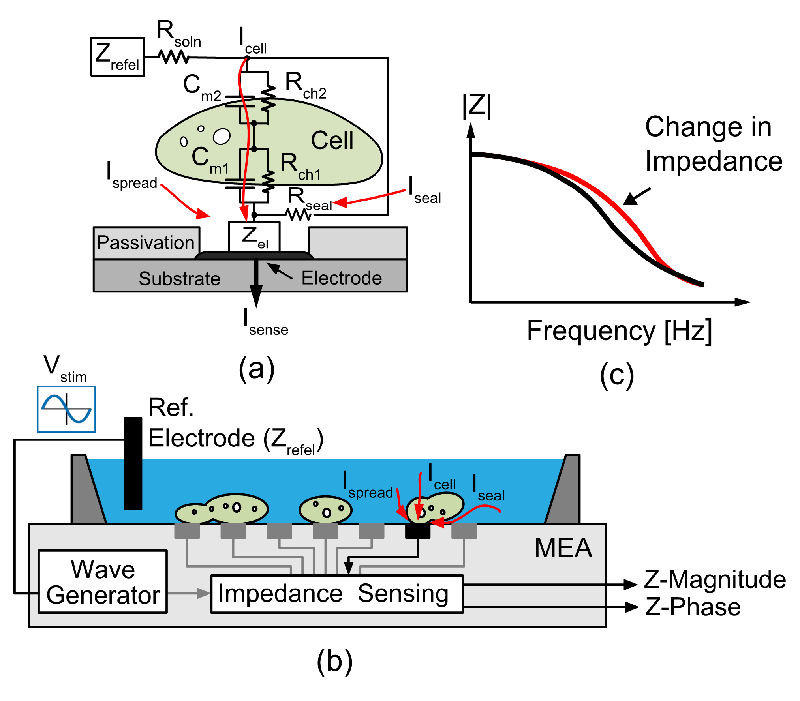
(a) Cell impedance model, (b) principle of EIS measurements and setup, (c) EIS response graph.
Impedance measurements can be performed either by applying an AC voltage between the working electrode and a reference electrode in the solution and measuring the resulting current [3] [7], or by establishing an AC current and measuring the required voltage [13] [14]. For measurements in an array format with thousands of electrodes, the first mentioned method was preferred, as it enables to measure many electrodes in parallel and independently, as shown in Fig. 1.b. The cell-electrode impedance parameters can be estimated by measuring impedance changes of the electrode-electrolyte-cell interface over a wide frequency range (Fig. 1.c) [15] [16] [17].
B. Microelectrode Array
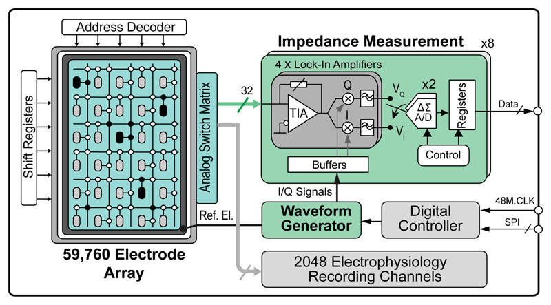
A simplified block diagram of the impedance-measurement units of the HD-MEA system is shown in Fig. 2. The overall system has been described in [11]. The system architecture critically relies on the switch-matrix (SM) approach [18], which makes it possible to perform impedance measurement and/or electrophysiology recordings with any arbitrarily selected electrodes or subsets of electrodes. The 59,760 working electrodes were arranged as pixels in 180 rows and 332 columns, at a center-to-center pitch of 13.5 μm. Each pixel consists of a platinum (Pt) electrode with a size of 7.5×3.0 μm2, four switches and three SRAM cells for configuring the switches. Electrode signal lines are all shielded with analog supply/ground tracks to minimize crosstalk. The reference electrode (area of 0.27 mm2) was placed at the periphery of the array. As the number of simultaneously useable impedance measurement channels is limited to 32, the electrode array can be configured either with sparsely distributed electrodes for overview measurements of a large preparation, or with the highest density for high-resolution measurements of single cells or cell assemblies. A full recording of an impedance image from all electrodes of the array will take approximately 1-2 minutes (details in Section IV). The array can be reconfigured in 4.5 ms by programming the SRAM cells.
Fig. 2.
Schematic of the HD-MEA system components designed to measure impedance characteristics.
C. Impedance Measurement Channels
All circuitry needed to conduct the impedance experiments has been integrated on chip (see Fig. 2). To perform impedance magnitude and phase measurements, the lock-in principle [19] was adopted. 32 lock-in amplifiers were integrated on chip to sense the impedance over a frequency range from 1 Hz to 1 MHz. Any electrode in the array can be routed to the lock-in amplifier owing to the implemented switch-matrix. To measure the impedance, on-chip generated sinusoidal voltages (with amplitudes between 10 and 40 mV) were applied to the reference electrode. The sinusoidal current signal arriving at the selected working electrodes, i.e., the sensing current, was then converted into a voltage by a transimpedance amplifier (TIA), and mixed with the in-phase and quadrature (I and Q) mixing signals, which were also generated by the waveform generator. The two output signals were then low-pass filtered to remove the higher-order intermodulation components. The output signals of every set of four lock-in amplifiers were multiplexed and digitized by two ΔΣ modulators. The bit streams of the two ΔΣ modulators were sent off chip and decimated in real-time by cascaded integrator-comb (CIC) filters that have been implemented in a LabVIEW program (details in Section IV). The impedance magnitude and phase were then extracted from the in-phase (VI) and quadrature (VQ) data as follows:
D. Electrophysiological Recordings
To simultaneously record electrophysiological activity of large cell preparations/networks together with impedance measurements, 2048 extracellular-action-potential (EAP) readout channels were integrated in the HD-MEA system. The EAPs usually have amplitudes on the order of hundreds of μV and feature a bandwidth between 300 Hz and 6 kHz. Each EAP recording channel consists of four fully differential amplification stages and a 10-bit successive-approximation register (SAR) analog/digital converter (ADC) to sample the channels at 20 ksamples/s. The total gain can be programmed in steps of 6 dB from 29 dB to 77 dB. For a detailed description of the AP-recording channel, please refer to [11][20][21].
III. Circuit Implementation
To measure impedance over a wide range of frequencies with a high dynamic range, the lock-in amplifier was designed to have a maximum trans-impedance of about 107 V/A, followed by an incremental-type ΔΣ-modulator-based analog-to-digital (A/D) conversion.
A. Lock-in Amplifier
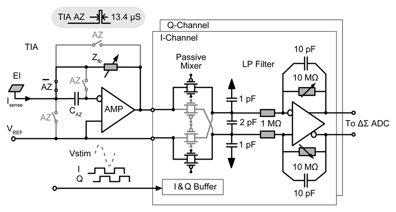
The lock-in amplifier, shown in Fig. 3, was realized with a low-noise TIA and in- and quadrature-phase mixers, followed by two low-pass filters (LPFs) for the I & Q channels, respectively.
Fig. 3.
Lock-in amplifier including a TIA, a passive mixer, and a low-pass filter.
To accommodate a wide impedance range (from 10 kΩ to 10 GΩ) for measuring various biological preparations (cultured cells, tissue slices, etc.), a TIA with programmable capacitive and resistive feedback was designed. The resistive feedback is suitable for measuring large electrodes (impedance < 100 MΩ). However, this kind of feedback features a tight noise-bandwidth trade-off, because the feedback resistance (Rf) sets both, a lower limit for the equivalent input current noise (4kT/Rf, where k and T denote the Boltzmann constant and the absolute temperature) and an upper limit for the TIA bandwidth due to the parasitic capacitance in parallel with Rf. To measure small electrodes with less than 10 μm diameter (impedance > 100 MΩ), the capacitive feedback is preferred, as it is not subjected to the above-mentioned trade-off. For the capacitive feedback, a periodic reset [22] [23] was necessary to prevent the TIA from attaining saturation and to stabilize the electrode potential at the reference voltage, VREF. To mitigate the drift of the electrode-electrolyte interface capacitor, Ce (which is known to be problematic and a source of error in all electrochemical sensors), and the amplifier offset, an auto-zeroing (AZ) function was implemented in the TIA. The most important capacitors in this TIA are the programmable feedback capacitor (Cf = 0.1, 1, 10 pF), the offset voltage storing capacitor (CAZ = 200 fF), and the electrode-electrolyte capacitor (Ce) with an electrolyte- and electrode-material-dependent unit capacitance (typically ~1.0 pF/μm2 for Pt electrodes). During the AZ phase (AZ is high in Fig. 3 and lasts 13.4 μs), the TIA’s offset was first stored in CAZ. Later, during the measurement phase (AZ is low, few ms), the sensing current was integrated on Cf, and the offset was cancelled at the TIA’s output (Fig. 3). The TIA employed a two-stage Miller-compensated amplifier, which achieved an open-loop gain of 120 dB and a gain-bandwidth (GBW) of 10 MHz.
A double-balanced passive mixer has been implemented for in-phase and quadrature demodulation of the TIA output signal (Fig. 3). Passive mixers feature a higher linearity and negligible 1/f noise compared to the respective active counterparts [24]. In addition, the mixer converted the single-ended output of the TIA into a differential signal, which was beneficial for the subsequent LPF and ΔΣ modulators, as differential signals are less prone to power-supply and substrate interference. The differential structure also helped to reduce the charge injection due to switching. Since the passive mixer had an inherent conversion loss of 2/π [25], a sufficient voltage swing was established by programming the TIA gain before mixing.
An active fully-differential LPF was employed to remove high-frequency spurs, generated by the mixer before (A/D) conversion. Due to a high oversampling ratio (64), provided by the ΔΣ ADC, the anti-aliasing requirements were largely relaxed. The low-pass cutoff frequency was chosen to be 16 kHz, realized with a 10 pF feedback capacitor and a 10 MΩ resistor. By tuning the feedback resistance, the LPF gain could be adjusted in three modes: 1, 5, or bypass (Fig. 3). The fully-differential amplifier was implemented with a folded-cascode topology and a continuous-time common-mode feedback.
B. ΔΣ ADC
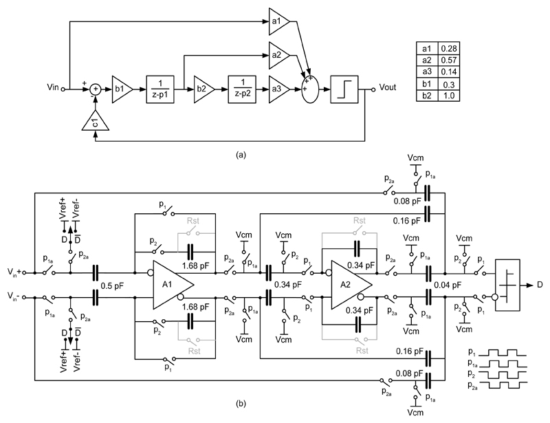
The output of the lock-in amplifier was digitized by an incremental single-bit ΔΣ ADC consisting of an on-chip ΔΣ modulator and an off-chip decimation filter. Instead of a continuous-time ADC, a switched-capacitor topology was chosen to take advantage of its good accuracy and linearity. To increase the input signal swing while relaxing the slewing requirements of the integrators, a cascade of integrators feedforward (CIFF) topology [26] was chosen (Fig. 4.a). By setting the sampling frequency to 750 kHz and the signal bandwidth to 5.8 kHz, an oversampling ratio of 64 was achieved, which is sufficiently high to guarantee a resolution of 16 bits with a time resolution of 0.17 ms, if proper filtering is used [7]. The schematic of the ΔΣ modulator is illustrated in Fig. 4.b. To meet the noise requirement, a large capacitor (1.68 pF) was used for sampling the input signal [27]. The flicker noise and offset of the first opamp in the ΔΣ modulator, which could deteriorate the mixer’s output containing the DC value to be converted, has been substantially reduced by implementing an auto-zeroed first-stage integrator [28]. Since the first-stage amplifier requires a high DC gain and large bandwidth, a fully-differential, folded-cascode amplifier with a switched-capacitor common-mode feedback was implemented with 92 dB DC gain and 3 MHz unity-gain bandwidth.
Fig. 4.
Delta-Sigma modulator: (a) block diagram and (b) circuit implementation.
C. Pipelined Multiplexing
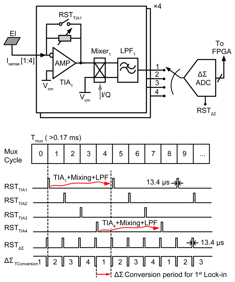
Incremental-type ΔΣ operation was necessary to multiplex signals from 4 lock-in amplifiers. In total, 16 ΔΣ modulators (8 for I & Q channels) were used for sampling the output signals from the 32 lock-in amplifiers. The ΔΣ conversion was designed in a pipelined fashion to increase the throughput. All memory elements, e.g., the switched-capacitor (SC) integrators in the ΔΣ modulator, were reset before a new lock-in amplifier operation started (e.g., Mux cycle 0), as shown in Fig. 5. Then, the TIA1 was reset (for the auto-zeroing operation in the case of the capacitive feedback). In the next three Mux cycles, the TIA and mixer converted the signal into the corresponding DC signal and also produced unwanted high-frequency spurs. These spurs were removed by the first-order LPF, with a time constant (τ) of 0.1 ms. At the start of 4th Mux cycle, the ΔΣ ADC began to convert the signal of the first lock-in amplifier. The signal bandwidth of the ΔΣ modulator was designed to be 5.8 kHz, which entailed a minimum Mux cycle period (Tmux) of 0.17 ms. For proper LPF settling, three Mux cycles were allocated (0.17 ms × 3 = 0.51 ms, which was about 5 τ and the LPF could settle to 99% of its final value). However, the Tmux had to be adapted to the frequency of the impedance measurement (fstim). For example, for an fstim of 1 kHz, considering an average of 10 sine periods for proper lock-in amplifier operation, Tmux >3 ms (10 ms / three Mux cycles). But for a 1 Hz impedance measurement, Tmux should be very long (>3 seconds). Hence, for each fstim we set the Tmux > 3/fstim, with a minimum value of 0.17 ms. Some bio-measurements require continuous impedance monitoring, for instance, measurements of cardiac cells [29]. For such cases, the TIA output could be directly digitized by the ΔΣ ADC without mixing and multiplexing (8 channels instead of 32). The impedance information could then be extracted off-chip by an FFT operation.
Fig. 5.
Delta-Sigma ADC sampling – pipelined multiplexing scheme.
Finally, bit streams from all the 8×2 ΔΣ ADCs at 750 kHz were temporarily stored in flip-flop banks. The data were rearranged as a parallel 8-bit, 1.5 MHz output and then, along with electrophysiology data frames (2048 channels at 20 ksamples/s), sent through the 10-bit system bus [11].
D. Waveform Generator
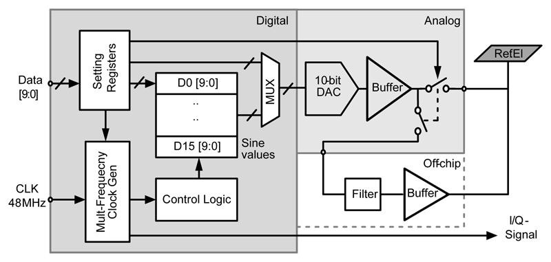
A programmable waveform generator was utilized to generate a stepwise approximation of the stimulation signal. The block diagram of the programmable waveform generator is shown in Fig. 6. The waveform generator included a multi-frequency clock generator, a setting register, an “on-chip look-up table” to store the sine-wave sampling values, a 10-bit R-2R DAC, and a voltage buffer. The multi-frequency clock generator divided the 48 MHz system clock for different sine-wave frequencies. The sine values, stored in the on-chip lookup table, could be programmed through the SPI interface to set the amplitude of the sinusoidal signal. The sine-wave generation technique was adapted from [30], where each quadrant of the sine wave was generated from 16 sampling values stored in the look-up table. A full period (64 data samples) was then generated from four quadrants by reversing the order of the stored values and changing their polarity with a control logic, taking advantage of the sine wave symmetry. The control logic also generated the I & Q signals in each quadrant, phase-locked to the sinusoidal signal. The waveform generator covered a frequency range from 1 Hz to 1 MHz. The maximum frequency was limited by the R-2R DAC, which had a conversion rate of up to 10 Msamples/s. Signals with frequencies above 128 kHz were, therefore, constructed by less than 64 samples (e.g., 32 samples for 256 kHz, 16 samples for 512 kHz, and 8 samples for 1.024 MHz). Since the number of samples/periods affects the signal quality, optional pads were included for applying a high-quality external sinusoidal signal and corresponding I & Q signals to the impedance measurement channels. The waveform generator occupied an area of 0.012 mm2 and dissipated 1.1 mW power from a 3.3 V supply when driving a load of 10 nF at 1 MHz. Our measurements demonstrated that the achieved phase error was less than 2 degrees over the frequency range from 1 Hz to 1 MHz.
Fig. 6.
Block diagram of the waveform generator.
IV. Electrical Characterization
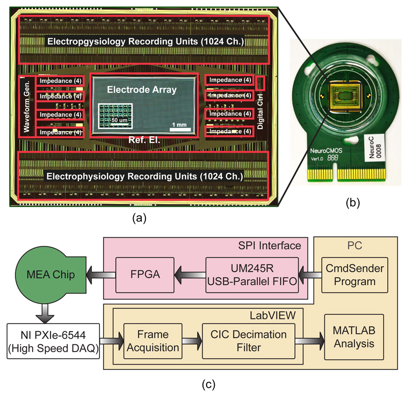
The chip was fabricated in a 6M1P 0.18-μm standard CMOS process, provided by XFab, Erfurt, Germany. The die size was 12×8.9 mm2, and the chip micrograph is shown in Fig. 7.a. The silicon area of one individual impedance measurement channel was about 0.1 mm2. A titanium-tungsten adhesion layer and platinum electrodes were post-processed at wafer level using ion-beam deposition and etching. Afterwards, a multilayer SiO2/Si3N4 passivation stack (4 layers of alternating Si-oxide and Si-nitride ending with Si-nitride) was deposited by plasma-enhanced chemical vapor deposition to protect the CMOS metal layers against the saline cell culture medium. The passivation stack was afterwards opened in the electrode areas and in the contact areas for wire bonding through a reactive-ion etching step. The chip was then packaged onto a custom PCB inside a bio-compatible plastic epoxy well (Fig. 7.b), in which dissociated cells, such as primary neurons, or brain slices along with culture solution could be accommodated.
Fig. 7.
Micrographs of (a) the overall system chip and (b) the packaged chip on a PCB. (c) Block diagram of the measurement setup.
The total power consumption of the chip including the waveform generator, all impedance channels and 2048 electrophysiology recording channels was 48 mW. On the HD-MEA a Pt-resistor, adjacent to the sensor array, was also fabricated during the post-processing step to monitor the temperature during experiments. The measurements yielded a temperature increase of less than 1°C (~0.85°C) when all the impedance channels and 2048 electrophysiology recording channels were powered up during the experiments described in Section V.
A block diagram of the measurement setup is shown in Fig. 7.c. A serial peripheral interface (SPI) was implemented to communicate with and configure the chip. In the SPI interface, a UM245R chip (Future Technology Devices International Ltd. (FTDI), Glasgow, United Kingdom) was used to create a USB-to-parallel interface, and an FPGA was used to store and send commands at 48 MHz. A program was developed in C# that generated different commands for configuring gains and bias currents of amplifiers, for setting the coefficients for the waveform generator and more. The 10-bit digital output data of the chip was acquired using an NI PXIe-6544 high-speed DAQ card.
A CIC decimator filter was designed and implemented in a LabVIEW program to extract the output bit streams of ΔΣ ADC. Considering the over sampling frequency which is 750 kHz and in order to remove high ordered frequency components of the mixing signal, parameters of the filter were determined to have the cut-off frequency lower than 1 kHz. These parameters include filter order (N), rate change factor (R), and differential delay (M). R was designed as 256 regarding to the number of available samples and M and N considered as 1 and 4, respectively to have a narrow bandwidth filter with cut-off frequency of 664 Hz. As the DC component of the signals are required to acquire the in-phase and quadrature parts of the impedance, a digital low-pass filter with 10 Hz bandwidth was applied on the signals, and then the average of last stable samples was calculated. Magnitude and phase of the impedance were then extracted from the in-phase (I) and quadrature (Q).
Since there are 32 parallel impedance measurement channels on chip, a full array scanning of the 59,760 electrodes at full spatial resolution will require ~1868 array configurations. As mentioned in Subsection III.C, the time required for each impedance measurement depended on the specified frequency and the number of cycles used for averaging. Therefore, low-frequency (<1 kHz) impedance measurements took a longer time. At higher frequencies, measurements could be performed in less time, but required at least 0.68 ms, as channel multiplexing and the ΔΣ conversion were required for each measurement. Thus, a full scan of the array at full spatial resolution takes approximately 1-2 minutes. As there are 2048 AP recording channels, a full electrophysiology scan of the whole array can be done with 30 array configurations, which takes only a few seconds.
A. Noise and Dynamic Range
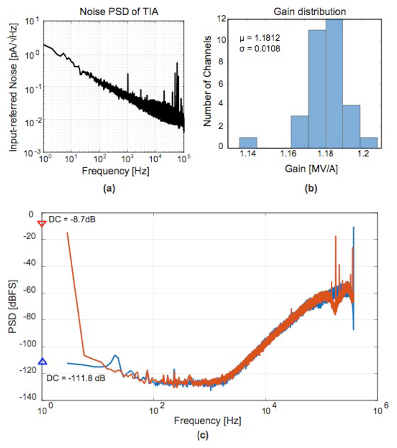
The input-referred current noise power spectral density (PSD) of the TIA with a 10 MΩ feedback resistor is shown in Fig. 8.a. The integrated current noise over a bandwidth between 1 Hz and 100 kHz was 6.4 pArms, which revealed a good current sensitivity of the reported EIS system. At low frequencies, the 1/f noise of the TIA dominated. The measured noise level is sufficient for most EIS applications, further improvements are limited by the thermal noise contribution from the electrode-electrolyte spreading resistance [31].
Fig. 8.
(a) Input-referred noise of the TIA; (b) TIA gain distribution (c) Measured output spectra of the delta-sigma ADC with shorted input (blue) and with an applied 1 V DC signal input (red).
The inter-channel gain variations were a major problem for multi-channel systems, which was primarily caused by the mismatches between the feedback resistors or capacitors of the TIAs and electrode-electrode impedance variations. The gain fluctuation across different channels, measured with a 1 MΩ load, was around ±3.24% (3-sigma) over the entire electrode array (Fig. 8.b). Before each biological measurement, the gain of each channel was measured, and later digitally compensated.
Fig. 8.c shows the noise PSD of the ΔΣ ADC, with a shorted input and a full-range 1 V DC input. The figure revealed a dynamic range of ~102 dB, which was equivalent to a 16-bit resolution and which determined the upper limit of the impedance range that could be measured. The total power consumption of each channel, including the ΔΣ ADC, was 412 μW. The overall performance and key metrics of the EIS system are compared in Table I.
Table I. Performance comparison with state-of-the-art EIS systems.
| Reference | [2] | [9] | [3] | [30] | [8] | This work |
| Topology | Resistive or SC TIA | TIA + Direct I/Q conversion | TIA + Direct I/Q conversion | SC TIA + Multiplying ADC | V/I sensing + Direct I/Q conversion | Lock-in + ΣΔ |
| Technology | 0.18 μm | 0.5 μm | 0.35 μm | 0.13 μm | 0.13 μm | 0.18 μm |
| Area (per Channel) | 0.02 mm2 | 0.06 mm2 | 0.01 mm2 | 0.06 mm2 | - mm2 | 0.1 mm2 |
| Sensing Area | 0.16 ×0.12 mm2 | 3×3 mm2 (estimation) | 1×1 mm2 | 1.05×1.6 mm2 | 9 pixel groups of 0.128 mm2 | 4.5×2.4 mm2 |
| No. of Electrodes | 5 × 10 | 100 (estimation) | 10 × 10 | 16 | 144 | 59,760 |
| Electrode Pitch | 150 μm | >600 μma | 100 μm | 300 μm | 89.4/357.8 μma | 13.5 μm |
| No. Channels | 50 | 100 | 100 | 16 | 144 | 32 |
| Impedance Range | - | - | 100 Ω - 100 MΩ | ~GΩ | 10 kΩ – 1 GΩ | 1 kΩ – 10 GΩ |
| Transduced Current Range | 0.1 nA – 250 μA | 78 fA – 100 nA | +/- 25 μA | Max. 400nA | - | 10 pA – 30 μA |
| Frequency Range | 20 Hz | 1 mHz – 10 kHz | 10 Hz – 50 MHz | 0.1 Hz – 10 kHz | 500 kHz – 4 MHz | 1 Hz – 1 MHz |
| Noise | 25 μVrms (1 Hz – 1 kHz) | - | 330 pArms (1 Hz – 10 Hz) 577 pArms (1 Hz – 1 kHz) | 320 fArms | - | 6.4 pArms (1 Hz – 100 kHz) |
| DR | - | 122 dB | 97 dB | 140 dB | - | 102 dB |
| Supply | 3.3 V | 3 V | 3.3 V | 1.2 V | 3.3 V | 3.3/1.8V |
| Power (per Channel) | 2.7 mW | 6 μV | 736 μV | 42 μVb | - | 412 μWb |
| Multiple Functions | - | - | - | - | Impedance, Voltage, optical | Impedance, Electrophysiology |
Equivalent square-shaped pixel dimension, for the same spatial density.
ADC included
B. Impedance Measurement of an RC Network
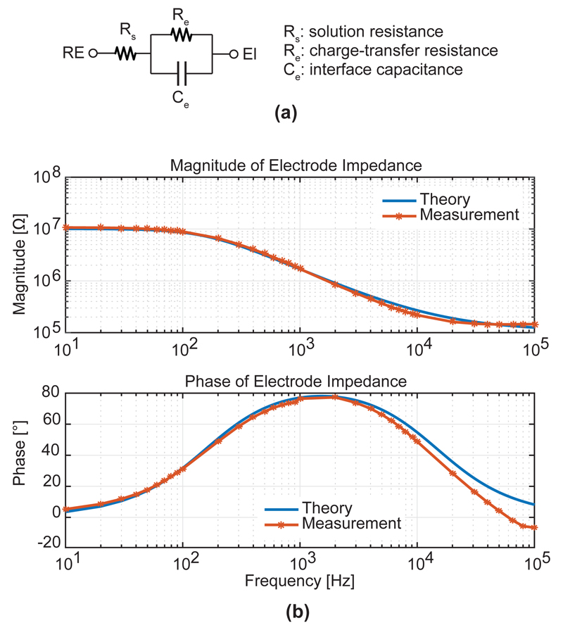
To validate the impedance measurement circuit, the input of a lock-in amplifier was disconnected from the electrode and connected to an external discrete RC network, which was arranged as an equivalent circuit for the electrode-electrolyte interface (Fig. 9.a). Values of Rs, Re, and Ce were chosen to be 110 kΩ, 10 MΩ, and 100 pF, respectively. The impedance of the RC network was measured over a frequency range from 10 Hz to 100 kHz and was compared to values obtained by theoretical calculations. It can be seen in Fig. 9.b that the measured values matched the theoretical values very well at low frequencies. At high frequencies above 10 kHz, small deviations from the theoretical values were found, likely caused by the parasitic capacitance and switch on-resistance of the long probe-input leads on the chip.
Fig. 9.
EIS System validation using an electrode-electrolyte equivalent circuit.
C. Electrode-electrolyte Impedance Measurements
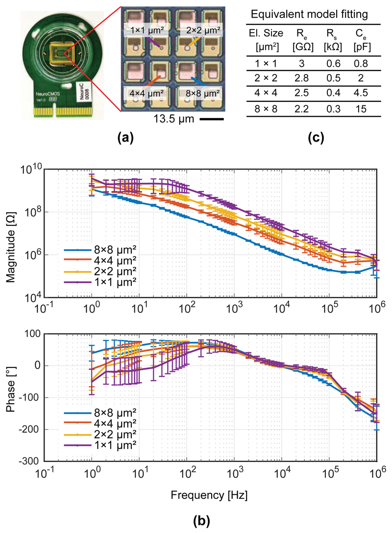
For electrochemical characterization, bright Pt electrodes of four different sizes (8×8 μm2, 4×4 μm2, 2×2 μm2, 1×1 μm2) were fabricated on the CMOS chip (Fig. 10.a). Impedance measurements of the electrodes were performed in a phosphate-buffered saline (PBS) solution, which had similar electrochemical properties as a physiological solution. As can be seen in Fig. 10.b, the impedance magnitude of the electrode-electrolyte interface showed a 1/f roll-off behavior, which indicated a dominance of the double-layer capacitance (Ce), as it could be expected in this (~kHz) frequency range. The impedance phase around 1 kHz ranged between 60 and 80 degrees and reflected the capacitive behavior of the electrodes. At frequencies above 10 kHz, the spreading resistance (Rs) started to dominate, and the impedance phase tended towards negative values. At frequencies below 10 Hz, the impedance was dominated by the charge-transfer resistance Re, in the GΩ range. The values of the equivalent-circuit components of the electrode-electrolyte for different electrode sizes were obtained from model fitting and are summarized in Fig. 10.c.
Fig. 10.
(a) Impedance values of bright Pt-electrodes of different size, (b) Impedance magnitude and phase values versus frequency; (c) Values of the different components, obtained from equivalent-model fitting.
V. Bio-Measurements
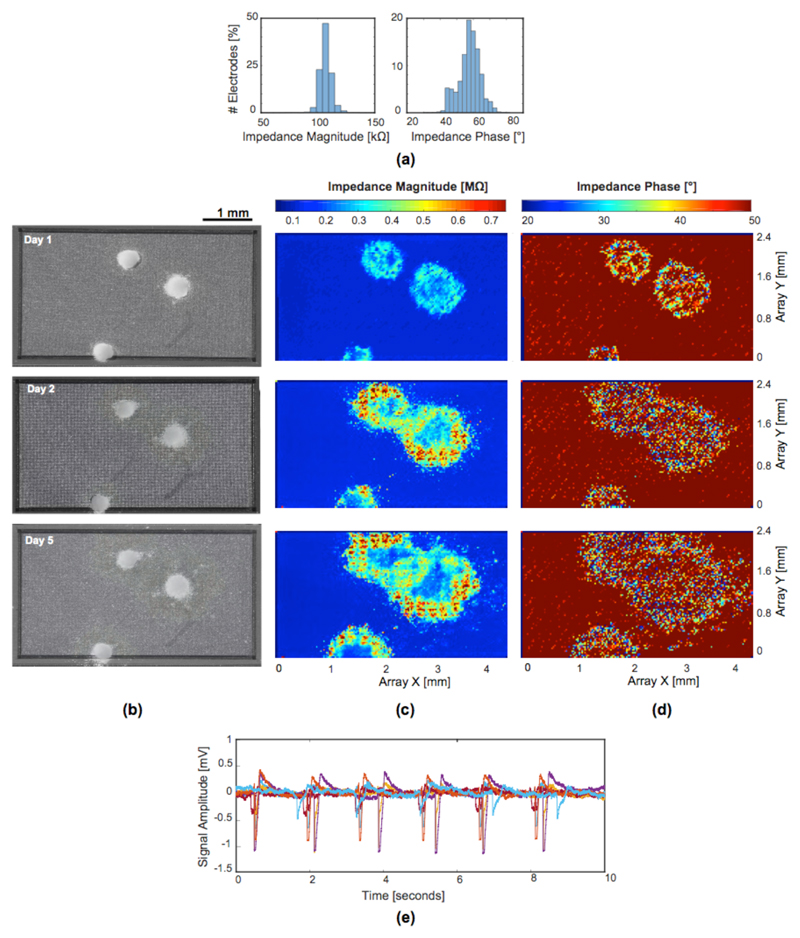
To demonstrate the performance of the EIS system, two impedance imaging bio-experiments were performed with (i) microtissues (embryoid bodies) and (ii) acute brain slices. All animal-cell work was approved and licensed by the Basel-City Cantonal Veterinary Authority following Swiss federal laws on animal welfare. For the bio-experiments an electrode size of 3×7.5 μm2 was used for both, impedance and electrophysiological measurements. Bright Pt electrodes of this size feature impedance magnitude values of 2.3±0.04 MΩ and phase values of 0.7±0.5 degrees at 10 kHz [11]. To reduce the impedance and, consequently, the thermal noise of the electrodes, Pt-black was electrodeposited before performing the bio-experiments [32] [33]. Pt-black deposition effectively increases the electrode surface area without increasing the geometrical electrode area. The impedance can be reduced 30-40 fold by applying Pt-black in comparison to bright Pt electrodes [11] [34]. Magnitude values of 107±5.2 kΩ and phase values of 57±6.5 degrees at 10 kHz were measured across all Pt-black electrodes in PBS before doing the bio-measurements (Fig. 11.a). Since Pt-black is mechanically not very stable, a homogeneous impedance across the array was achieved by re-depositing Pt-black and measuring the electrode impedances before each bio-experiment in order to be able to assess the spatial impedance features of cells or tissues.
Fig. 11.
Embryoid bodies (EBs) were placed onto the MEA surface, and EIS measurements were performed after cell placement. Pt-black-covered electrodes with a size of 3×7.5 μm2 were used for the bio-experiments. (a) Impedance magnitude and phase distribution of all electrodes at 10 kHz, measured in PBS before the bio-measurement. (b) Microscope images taken five days after the beginning of EB formation and on the 1st, 2nd, and 5th day of EB placement on the chip. (c) Plots of the impedance magnitude values, measured by the full array of electrodes (56,320 electrodes were used in 1760 electrode configurations) on the same days, covering initial cell attachment until full EB adhesion. (d) Corresponding impedance phase values. (e) Electrophysiological recordings (cardiac beating) of the differentiated EBs measured through several electrodes after 5 days of adhesion and culturing on the chip.
A. Cardiac Cells in Embryoid Bodies
In this experiment, mouse embryonic stem cells (mESC) were first cultured in hanging drops [35] to form three-dimensional multicellular aggregates, called embryoid bodies (EBs). The cardiac differentiation of the EBs was monitored by using impedance measurements and electrophysiological sensing. In the first five days, the EBs were differentiated in the suspension culture. Afterwards, the EBs were plated on the HD-MEA electrode surface, precoated with Fibronectin (Sigma-Aldrich GmbH), where they could adhere and spread.
The microscopic images in Fig. 11.b were taken on the 1st, 2nd, and 5th day of EB adhesion on the electrode array. For the impedance measurements, the HD-MEA was placed in an incubator with 36°C and low humidity to prevent damage to the electronics. Evaporation of the medium was averted by placing lids over the chips. Impedances of the array (56,320 electrodes) was measured at 10 kHz by scanning through 1760 array configurations. In each configuration 32 electrodes could be measured simultaneously. It took three seconds to re-route the electrode array for each configurations (due to software rather than hardware limitations) and one second for recording the impedance data. In total the full array impedance scanning took about two hours. The position of the embryoid bodies and the involved cells, their adhesion, spreading and growth could be clearly identified according to the measured impedance changes, both in magnitude and phase (Fig. 11.c, 11.d). During these five days, the cells at the tissue circumference did spread out and formed a thin layer, which attached tightly to the electrode array. This tight attachment most probably resulted in higher impedance values over time as shown in Fig 11(c). We observed that the impedance remained almost the same at the center of the tissue, between day 1 and day 5 (Fig 11(c)). After five days of adhesion, electrophysiological activity of the differentiated EBs could be recorded by using the EAP recording channels. Fig. 11.e shows electrical activity recorded through several electrodes under the embryoid bodies, featuring an average beating rate of 36 per minute.
B. Acute Brain Slices
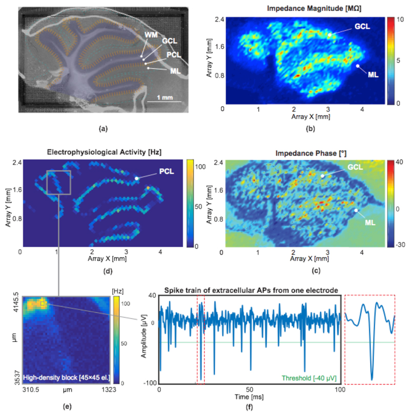
To perform impedance imaging of different cell layers in brain tissue, an acute cerebellar slice of a wild-type C57b/6 mouse (Charles River Laboratories) was placed on the HD-MEA (Fig. 12.a). The slice was perfused using carbogen-loaded Artificial Cerebrospinal Fluid (ACSF) at 36°C to keep it viable for the duration of the measurements. As illustrated in Fig. 12.a, four main cell layers could be differentiated: 1) white matter (WM) that consists of axons, climbing fibers and mossy fibers, mostly without electrogenic cells, 2) the granular cell layer (GCL) featuring a high density of granular cells, 3) the Purkinje cell layer (PCL), which contains Purkinje neurons with high electrophysiological activity, and 4) the molecular layer (ML) which contains the fan-shaped dendritic trees of Purkinje cells and parallel fibers. The impedance measurements were performed at 10 kHz with 110 different electrode configurations to acquire the impedance information from 3520 uniformly distributed electrodes on the array (every 4th electrode). The impedance magnitude and changes in the impedance phase before and after placing the slice are shown in Fig. 12.b and Fig. 12.c, respectively. Different cell layers could be easily distinguished in these impedance images. For instance, the granular cell layer with high cell density exhibited larger impedance magnitudes [36][37] than less dense layers.
Fig. 12.
Impedance imaging and electrophysiological activity of an acute mouse cerebellar brain slice placed on the HD-MEA. Pt-black-covered electrodes with a size of 3×7.5 μm2 were used for the bio-experiment (a) Microscopic image of the cerebellar slice. The dark regions show the white matter (WM), granular cell layers (GCL) are marked in blue, Purkinje cell layers (PCL) are marked in orange, and molecular layers (ML) are marked in cyan. (b, c) Impedance magnitude and difference in phase values, measured from the electrodes. To cover the entire array, impedance measurements were repeated with 110 different electrode configurations using 3520 uniformly distributed (every 4th) electrodes. (d) Electrophysiological activity, action potential (AP) activity recorded from 2000 sparsely configured electrodes by AP recording channels. (e) High-density recording from an active region recorded by 45×45 electrodes.(f) electrophysiological signals (spike train) obtained from one of the electrodes.
Fig. 12.d shows spontaneous electrical activity of Purkinje neurons of the slice recorded during 20 s. One sparse electrode configuration was used in which 2000 uniformly distributed electrodes were connected to the on-chip EAP recording channels. Fig. 12.e shows a highest-resolution close-up of an active region, recorded with 45×45 electrodes in high-density configuration. The use of the highest possible electrode resolution enables subcellular-spatial-resolution electrical and impedance recordings of brain slices. The EAP signal amplitudes are to a large extent depending on the tissue-electrode attachment, nevertheless, the recorded EAP signals featured good signal-to-noise ratios of more than 10 (Fig. 12.f, see also individual EAP on the right).
VI. Conclusion
In this paper, we presented a CMOS HD-MEA system that can perform electrochemical impedance spectroscopy (EIS) along with electrophysiology recordings on 59,760 electrodes at 13.5 μm spatial resolution. The circuitry was fabricated in a standard 0.18 μm CMOS process. The impedance measurement circuits consumed only 412 μW per channel at 3.3 V supply and occupied only 0.1 mm2 per channel. All circuits needed to perform impedance and electrophysiology experiments were integrated on the chip. Impedances ranging between 10 kΩ and 10 GΩ could be measured by 32 on-chip lock-in amplifiers, which rendered the system suitable for characterizing a variety of biological preparations. We demonstrated the system capability to investigate and monitor position, adhesion, size, and electrical activity of embryoid bodies, and to conduct topographic impedance measurements of brain slices. The possibility to perform high-resolution impedance sensing in combination with electrophysiology recording render the reported HD-MEA system a versatile tool for in-depth studies of cellular behavior and dynamics.
Acknowledgments
The authors thank S. Geissler for help with preparing the manuscript, A. Stettler at ETH Zurich for the electrode post-processing, Evi Bieler at the University of Basel for providing the SEM image. The funders had no role in study, design, data collection and analysis, decision to publish, or preparation of the manuscript.
This work was supported by the ERC Advanced Grants 694829 “neuroXscales” (H2020) and 267351 “NeuroCMOS” (FP7). R. Bounik received individual support through the Swiss National Science Foundation, MHV-Grant 171267 and A. Shadmani was supported by the Grant FP7-MTN “EngCaBra” (Contract 264417).
References
- [1].Daniels JS, Pourmand N. Label-free impedance biosensors: Opportunities and challenges. Electroanalysis. 2007;19(12):1239–1257. doi: 10.1002/elan.200603855. [DOI] [PMC free article] [PubMed] [Google Scholar]
- [2].Hassibi A, Lee TH. A programmable 0.18 μm CMOS electrochemical sensor microarray for biomolecular detection. IEEE Sens J. 2006;6(6):1380–1388. [Google Scholar]
- [3].Manickam A, Chevalier A, McDermott M, Ellington AD, Hassibi A. A CMOS electrochemical impedance spectroscopy (EIS) biosensor array. IEEE Trans Biomed Circuits Syst. 2010;4(6 PART 1):379–390. doi: 10.1109/TBCAS.2010.2081669. [DOI] [PubMed] [Google Scholar]
- [4].Chen Y, Wong CC, Pui TS, Nadipalli R, Weerasekera R, Chandran J, Yu H, Rahman ARA. CMOS high density electrical impedance biosensor array for tumor cell detection. Sensors Actuators, B Chem. 2012;173:903–907. [Google Scholar]
- [5].Elshafey R, Tlili C, Abulrob A, Tavares AC, Zourob M. Label-free impedimetric immunosensor for ultrasensitive detection of cancer marker Murine double minute 2 in brain tissue. Biosens Bioelectron. 2013;39(1):220–225. doi: 10.1016/j.bios.2012.07.049. [DOI] [PubMed] [Google Scholar]
- [6].Guo J, Ng W, Yuan J, Chan M. A 51fA/Hz0.5 low power heterodyne impedance analyzer for electrochemical impedance spectroscopy. VLSI Circuits (VLSIC), 2013 Symp; 2013. pp. 56–57. [Google Scholar]
- [7].Gozzini F, Ferrari G, Sampietro M. An instrument-on-chip for impedance measurements on nanobiosensors with attofarad resolution. Dig Tech Pap - IEEE Int Solid-State Circuits Conf; 2009. pp. 346–348. [Google Scholar]
- [8].Chi T, Park JS, Butts JC, Hookway TA, Su A, Zhu C, Styczynski MP, McDevitt TC, Wang H. A Multi-Modality CMOS Sensor Array for Cell-Based Assay and Drug Screening. IEEE Trans Biomed Circuits Syst. 2015 Dec;9(6):801–814. doi: 10.1109/TBCAS.2015.2504984. [DOI] [PubMed] [Google Scholar]
- [9].Yang C, Jadhav SR, Worden RM, Mason AJ. Compact Low-Power Impedance Extractor and Digitizer for Sensor Array Microsystems. IEEE J Solid State Circuits. 2009;44(10):2844–2855. [Google Scholar]
- [10].Guo J, Ng W, Yuan J, Li S, Chan M. A 200-Channel Area-Power-Efficient Chemical and Electrical Dual-Mode Acquisition IC for the Study of Neurodegenerative Diseases. IEEE Trans Biomed Circuits Syst. 2016;10(3):567–578. doi: 10.1109/TBCAS.2015.2468052. [DOI] [PubMed] [Google Scholar]
- [11].Dragas J, Viswam V, Shadmani A, Chen Y, Bounik R, Stettler A, Radivojevic M, Geissler S, Obien MEJ, Müller J, Hierlemann A. In Vitro Multi-Functional Microelectrode Array Featuring 59 760 Electrodes, 2048 Electrophysiology Channels, Stimulation, Impedance Measurement, and Neurotransmitter Detection Channels. IEEE J Solid-State Circuits. 2017;52(6):1576–1590. doi: 10.1109/JSSC.2017.2686580. [DOI] [PMC free article] [PubMed] [Google Scholar]
- [12].Franks W, Schenker I, Schmutz P, Hierlemann A. Impedance characterization and modeling of electrodes for biomedical applications. IEEE Trans Biomed Eng. 2005 Jul;52(7):1295–1302. doi: 10.1109/TBME.2005.847523. [DOI] [PubMed] [Google Scholar]
- [13].Yúfera A, Leger G, Rodriguez-Villegas EO, Muñoz JM, Rueda A, Ivorra A, Gomez R, Noguera N, Aguiló J. An integrated circuit for tissue impedance measure. Proc 2nd Annu Int IEEE EMBS Special Topic Conf Microtechnologies Med and Biol; Madison, WI. May 2–4, 2002; pp. 88–93. [Google Scholar]
- [14].Min M, Parve T, Kukk V, Kuhlberg A. An implantable analyzer of bio impedance dynamics: mixed signal approach. IEEE Trans Instrum Meas. 2002;51:674–678. [Google Scholar]
- [15].Guo J, Yuan J, Chan M. Modeling of the Cell-Electrode Interface Noise for Microelectrode Arrays. 2013;6(6):605–613. doi: 10.1109/TBCAS.2012.2189569. [DOI] [PubMed] [Google Scholar]
- [16].Joye N, Schmid A, Leblebici Y. Neurocomputing Electrical modeling of the cell – electrode interface for recording neural activity from high-density microelectrode arrays. Neurocomputing. 2009;73(1–3):250–259. [Google Scholar]
- [17].Buitenweg JR, Rutten WLC, Willems WPA, Van Nieuwkasteele JW. Measurement of sealing resistance of cell-electrode interfaces in neuronal cultures using impedance spectroscopy. Med Biol Eng Comput. 1998;36(5):630–637. doi: 10.1007/BF02524436. [DOI] [PubMed] [Google Scholar]
- [18].Frey U, Sedivy J, Heer F, Pedron R, Ballini M, Mueller J, Bakkum D, Hafizovic S, Faraci FD, Greve F, Kirstein KU, Hierlemann A. Switch-matrix-based high-density microelectrode array in CMOS technology. IEEE J Solid-State Circuits. 2010;45(2):467–482. [Google Scholar]
- [19].Meade ML. Lock-in Amplifiers: Principles and Applications. London, U.K.: Peregrinus; 1983. reprint 1989. [Google Scholar]
- [20].Viswam V, Dragas J, Shadmani A, Chen Y, Stettler A, Mueller J, Hierlemann A. Multi-functional microelectrode array system featuring 59,760 electrodes, 2048 electrophysiology channels, impedance and neurotransmitter measurement units. 2016 IEEE International Solid-State Circuits Conference (ISSCC); 2016. pp. 394–396. [DOI] [PMC free article] [PubMed] [Google Scholar]
- [21].Viswam V, Chen Y, Shadmani A, Dragas J, Bounik R, Milos R, Müller J, Hierlemann A. 2048 action potential recording channels with 2.4μVrms noise and stimulation artefact suppression. Biomedical Circuits and Systems Conference (BioCAS); Oct. 2016; [DOI] [PMC free article] [PubMed] [Google Scholar]
- [22].Crescentini M, Bennati M, Carminati M, Tartagni M. Noise limits of CMOS current interfaces for biosensors: A review. IEEE Trans Biomed Circuits Syst. 2014;8(2):278–292. doi: 10.1109/TBCAS.2013.2262998. [DOI] [PubMed] [Google Scholar]
- [23].Manickam A, Singh R, Wood N, Li B, Ellington A, Hassibi A. A fully-electronic charge-based DNA sequencing CMOS biochip. 2012 Symposium on VLSI Circuits (VLSIC); 2012. pp. 126–127. [Google Scholar]
- [24].Zhou S, Chang MCF. A CMOS passive mixer with low flicker noise for low-power direct-conversion receiver. IEEE J Solid-State Circuits. 2005;40(5):1084–1093. [Google Scholar]
- [25].Razavi Behzad. RF Microelectronics. (2nd Edition) Prentice Hall Press; Upper Saddle River, NJ, USA: 2011. [Google Scholar]
- [26].Quiquempoix V, Deval P, Barreto A, Bellini G, Márkus J, Silva J, Temes GC. A low-power 22-bit incremental ADC. IEEE J Solid-State Circuits. 2006;41(7):1562–1571. [Google Scholar]
- [27].Schreier Richard, Temes Gabor C. Understanding Delta-Sigma Data Converters. Wiley-IEEE Press; 2004. Nov, [Google Scholar]
- [28].Wu R, Chae Y, Huijsing JH, Makinwa KAA. A 20-b ±40-mV range read-out IC with 50-nV offset and 0.04% gain error for bridge transducers. IEEE J Solid-State Circuits. 2012;47(9):2152–2163. [Google Scholar]
- [29].Bürgel SC, Diener L, Frey O, Kim J-Y, Hierlemann A. Automated, Multiplexed Electrical Impedance Spectroscopy Platform for Continuous Monitoring of Microtissue Spheroids. Anal Chem. 2016 Nov;88(22):10876–10883. doi: 10.1021/acs.analchem.6b01410. [DOI] [PMC free article] [PubMed] [Google Scholar]
- [30].Mazhab-jafari H, Soleymani L, Genov R. 16-Channel CMOS Impedance Spectroscopy DNA Analyzer with Dual-Slope Multiplying ADCs. 2012;6(5):468–478. doi: 10.1109/TBCAS.2012.2226334. [DOI] [PubMed] [Google Scholar]
- [31].Hassibi A, Vikalo H, Hajimiri A. On noise processes and limits of performance in biosensors. J Appl Phys. 2007;102(1):14909. [Google Scholar]
- [32].Bakkum DJ, Frey U, Radivojevic M, Russell TL, Müller J, Fiscella M, Takahashi H, Hierlemann A. Tracking axonal action potential propagation on a high-density microelectrode array across hundreds of sites. Nat Commun. 2013 Jul;4:2181. doi: 10.1038/ncomms3181. [DOI] [PMC free article] [PubMed] [Google Scholar]
- [33].Viswam V, Obien M, Frey U, Franke F, Hierlemann A. Acquisition of bioelectrical signals with small electrodes. Proceedings of the IEEE Biomedical Circuits and Systems Conference, BioCAS; 2017; 2018. Jan, pp. 1–4. [DOI] [PMC free article] [PubMed] [Google Scholar]
- [34].Viswam V, Bounik R, Shadmani A, Dragas J, Boos AJ, Birchler A, Müller J, Chen Y, Hierlemann A. High-density CMOS Microelectrode Array System for Impedance Spectroscopy and Imaging of Biological Cells. IEEE Sensors Conference; Orlando, Florida. 2016. [Google Scholar]
- [35].Frey O, Misun PM, Fluri Da, Hengstler JG, Hierlemann A. Reconfigurable microfluidic hanging drop network for multi-tissue interaction and analysis. Nat Commun. 2014 May;5:4250. doi: 10.1038/ncomms5250. [DOI] [PubMed] [Google Scholar]
- [36].Yedlin M, Kwan H, Murphy JT, Nguyen-Huu H, Wong YC. Electrical conductivity in cat cerebellar cortex. Exp Neurol. 1974;43(3):555–569. doi: 10.1016/0014-4886(74)90195-2. [DOI] [PubMed] [Google Scholar]
- [37].Okada YC, Huang JC, Rice ME, Tranchina D, Nicholson C. Origin of the apparent tissue conductivity in the molecular and granular layers of the in vitro turtle cerebellum and the interpretation of current source-density analysis. J Neurophysiol. 1994;72(2):742–53. doi: 10.1152/jn.1994.72.2.742. [DOI] [PubMed] [Google Scholar]


