Abstract
This work presents a fully integrated neural interface system in a small form factor (1.9 g), consisting of a μLED silicon optoelectrode (12 μLEDs and 32 recording sites in a 4-shank configuration), an Intan 32-channel recording chip, and a custom optical stimulation chip for controlling 12 μLEDs. High-resolution optical stimulation with approximately 68.5 nW radiant flux resolution is achieved by a custom LED driver ASIC, which enables individual control of up to 48 channels with a current precision of 1 μA, a maximum current of 1.024 mA, and an update rate of > 10 kHz. Recording is performed by an off-the-shelf 32-channel digitizing front-end ASIC from Intan®. Two compact custom interface PCBs were designed to link the headstage with a PC. The prototype system demonstrates precise current generation, sufficient optical radiant flux generation (𝚽e > 0.16 μW), and fast turn-on of μLEDs (trise < 10 μs). Single animal in vivo experiments validated the headstage’s capability to precisely modulate single neuronal activity and independently modulate activities of separate neuronal populations near neighboring optoelectrode shanks.
Keywords: in vivo electrophysiology, optogenetics, neural probe, headstage, micro-LED, LED driver, closed-loop, ASIC
I. INTRODUCTION
OPTOGENETICS has become a popular and powerful tool for neuroscience research since its introduction in 2005 [1]. The technique utilizes advances in genetic engineering and optics to provide precise resolution and cell specificity to modulate target neurons. The technique genetically modifies specific types of neurons to express light-sensitive ion channels, called opsins, on their membranes. The light-sensitive ion channels then provide means to selectively excite or inhibit neurons with light at specific wavelengths. Neural activity can thus be precisely modulated by controlling the amount of light delivered to the membranes of the neurons.
Due to the complexity and plasticity of the brain, a complete and robust interface requires not only state-of-the-art hardware but also advanced experimental protocols. More recently, many neuroscientists are adopting closed-loop control systems for optogenetics experiments, in which the stimulation parameters are automatically adjusted and controlled by the recorded signals [2], [3]. Closed-loop operation may not only enhance the established experimental techniques but also enable a new application space. Rapid and precise feedback can guide perturbations of neural systems, generating and confirming circuit-based models of underlying neuronal networks.
A compact bidirectional neural interface can be applied to optogenetic systems, where neural activities are optically modulated and electrically monitored. Researchers have developed a variety of such interfaces ranging from multi-functional optical fibers [4] to transparent shanks in a Utah probe-like arrays [5]. More recently, several groups have attempted to integrate small light sources and recording electrodes onto small microfabricated probe shanks [6]–[8]. Our group monolithically integrated several neuron-size (~10 μm) light-emitting-diodes (μLED) precisely positioned in the vicinity of recording sites within photolithographical resolution (< 1μm), enabling high-spatial-resolution optical stimulation and electrical recording for local circuit analysis [7].
In addition to the physical implantable probe arrays, a custom electronic system is required to interface the transducers with a host controller for closed-loop optogenetic studies. The light sources need to be driven by precise current sources with real-time control of amplitude, timing and shape. Simultaneously, neural recording front-ends should be able to amplify, digitize, and transmit the recorded signals to the host with high fidelity.
To date, the commercial systems such as Plexon’s PlexBright or Blackrock’s CerePlex’s offer optogenetic stimulation capabilities, but in a large form factor and limited channel counts. A few publications have attempted to scale down the size of system by integrating active circuitry on a headstage. In [9], a 2 channel stimulator chip was designed for a wireless fiber-based optogenetic stimulation system, while in [10] and [11], commercial off-the-shelf (COTS) components were integrated on miniature printed circuit boards (PCBs) to perform the same function. While these systems achieve significant size reductions, they suffer from low stimulation channel count and no recording capability. [12] proposed to increase the stimulation channel count by placing 18 μLEDs on a CMOS-fabricated probe shank with a fully-integrated electronic back-end. In [13], a μLED-coupled waveguide microneedle array probe was integrated with a wireless LED driver ASIC, but a separate commercial recording system was used to interface with the recording sites over long wire leads, preventing the system’s use in behavioral studies. [14] has included an on-board a COTS amplifier chip for neural recording in addition to the LED drivers. However, the system’s capabilities are reduced by a bulky single-channel light source. Systems in [15]–[17] introduced full wireless capability to the bidirectional headstage concept; however, the use of COTS components and probes, and the limitations of wireless transceivers hinder high channel count integration. In [18], a custom 6-recording-channel and 4-stimulation-channel probe-back-end chip is used to provide high-precision control for a hybrid LED/recording site electrode. The probe and the system, however, were not verified in vivo.
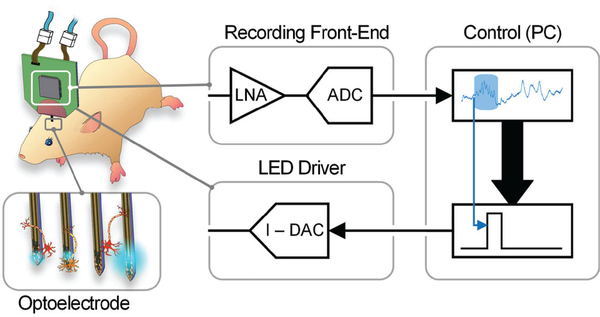
While the aforementioned systems have made big strides in miniaturization and improvement of bidirectional opto-electrophysiology, there is still an unmet need for a high-resolution, high-channel-count system with real-time stimulation control and a compact form factor allowing behavioral studies in rodents. To achieve this goal, we present a new optogenetics headstage suitable for our high density μLED optoelectrodes ([7], [19]) which integrates custom ASICs on a small light-weight printed circuit board (PCB) [20]. This headstage enhances the performance as compared with the current state-of-the-art works by: (1) scaling the number of stimulation and recording channels of the complete integrated electronic interface by a factor of 2, (2) providing more precise real-time optical stimulation control within a 1 μA LED current (or approximately 42.4 nW output radiant flux), and (3) reducing the system mass below 2 g for freely-moving in vivo mouse experiments. Fig. 1 shows the conceptual drawing of the proposed headstage, the peripheral interface modules and the μLED optoelectrode configuration. The remaining contents of the paper offer an in-depth description of the system implementation, benchtop tests, and in vivo validation experiments. Section II describes the system architecture and the host controller. Section III explains the headstage hardware design including custom integrated circuits for optical stimulation. Section IV provides the results of benchtop system characterization. In section V, in vivo experimental results are shown. Section VI provides a discussion and a path for complete closed-loop system implementation. Finally, the conclusions are summarized in section VII.
Fig. 1.
Schematic diagram of the opto-electrophysiology system in closed-loop configuration.
II. SYSTEM ARCHITECTURE
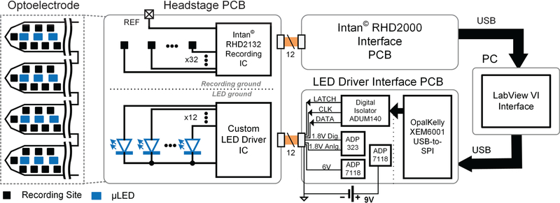
The complete hardware system consists of four main modules as shown in Fig. 2: (1) the headstage PCB, (2) LED driver interface board, (3) Intan® RHD2000 USB interface, and (4) the host PC.
Fig. 2.
System circuit diagram showing the connections between the headstage PCB with integrated optoelectrode and recording and LED driver ICs, interface boards providing power and communication for the recording and LED driver ICs, and the PC-based LabView VI Interface.
A. Headstage
The headstage is composed of a small form factor PCB integrated with the optoelectrode and interfacing ASICs. The optoelectrode contains 12 μLEDs and 32 recording sites in a 4-shank configuration [7], [19]. Each μLED is driven by separate anode connection and shares a common cathode (or the μLED ground). The recording reference node is routed off-board to a headstage fixture and an animal reference electrode.
The μLEDs are driven by a custom ASIC (described in more detail in section III.B) for channel-specific current driving with precise timing and amplitude control. The recording is performed by an off-the-shelf digital electrophysiology interface chip (RHD2132) from Intan Technologies. The two ICs are assembled and placed near the optoelectrode to minimize the distance from the stimulation and recording sites. The short distance between the μLEDs and the driver chip reduces the parasitic capacitance and inductance, thus minimizing the rise time and overshoot of the input current pulse. Likewise, the short recording channel traces reduce parasitic capacitances and interference in the recording circuit. The stimulation and recording grounds are separated on the headstage and throughout the entire system. This eliminates any possible high frequency noise in the recording channels coupled from the μLED current return path. The headstage is connected to the peripheral control modules via two cables, each carrying digital control signals and power and ground to the ASICs. Thin, flexible 12-wire cables with compact, lightweight connectors are used to minimize the tethering force to the animal’s head during experiments.
B. Peripheral Components
The μLED driver IC is powered and controlled through a custom driver interface module. System power is provided by a 9 V battery. Analog Devices ADP323 voltage regulator is used to provide 1.8 V, supplying the power to both analog and digital control circuits in the driver IC, while the ADP7118 voltage regulator provides the 6 V supply to the μLED current output nodes. An OpalKelly XEM6001 FPGA module converts the USB packets from the PC into an SPI-based protocol to communicate with the chip. Analog Devices ADuM140 digital isolator is used to transform the digital signals into a separate power and ground domain, isolating the stimulation system ground on the headstage PCB from the PC ground.
The recording chip is powered and controlled through an Intan® RHD2000 USB interface board. The board uses an OpalKelly XEM6010 FPGA for control and data acquisition between the Intan® RHD2132 recording IC and the PC.
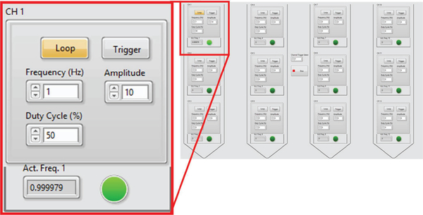
A custom LabVIEW graphical user interface (GUI) is developed for easy and precise control of the μLEDs, as shown in Fig. 3. Each μLED can be individually programmed and controlled to generate a pulse train of current at a given frequency and duty cycle. The μLEDs can be also configured to respond in real-time by onscreen button clicks or external triggers.
Fig. 3.
LabVIEW-based user interface for individual μLED control. In the inset, the channel 1 μLED located on top of the leftmost shank is configured to pulse at 1Hz frequency with 50% duty cycle and 10μA current amplitude.
III. HEADSTAGE HARDWARE DESIGN
A. μLED Optoelectrode
The optoelectrode is designed for high-spatial-resolution optical stimulation and electrical recording from a small region of the brain with high neuron density, such as the hippocampus. We monolithically integrated neuron-sized μLEDs (10 μm by 16 μm) and electrodes on the tips of fine silicon shanks in the typical ‘Michigan Probe’ configuration [7], [19]. GaN-on-Silicon wafers with epitaxially grown InGaN multi-quantum-wells (MQWs) were used to from the mesa structure of μLEDs.
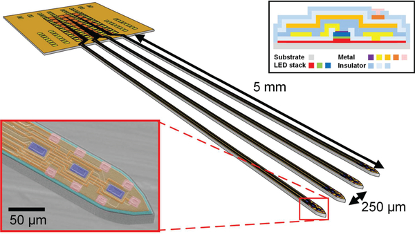
The dimensions of the optoelectrode and the layout of μLEDs and the recoding sites are shown in Fig. 4. The optoelectrode has four 5-mm long, 40-μm thick, and 70-μm wide silicon shanks. Shanks are 250 μm apart from one another, providing sufficient coverage of hippocampus by a single insertion. Each shank contains three blue (λpeak = 460 nm) InGaN MQW μLEDs vertically spaced by 60 μm and eight iridium electrodes vertically spaced by 20 μm.
Fig. 4.
Schematic diagram of the μLED optoelectrode. The insets show (bottom left) SEM image of the tip of a shank of the fabricated optoelectrode with coloring for visualization and (top right) the cross-section of the optoelectrode [19]. Modified from [20].
As shown in the cross-sectional schematic diagram (Fig. 4, top right inset), there are multiple metal layers integrated on the optoelectrode. The interconnection lines (interconnects) for the μLEDs are shielded by a dedicated EMI shielding ground layer. The μLEDs are connected in a common cathode configuration, so that each μLEDs can be individually controlled by the respective current source while the grounds are shared. The EMI shielding layer provides an additional ground plane for the electric field generated from the μLED cathode interconnection layer to minimize any possible electric field-induced interference.
Micromachining techniques that are used for fabrication of the Michigan Probes were slightly modified and utilized for μLED optoelectrode fabrication. The μLED mesa structures and the interconnects were defined on GaN-on-Si wafers (NovaGaN). The EMI-shielding metal layer was deposited and patterned, following a blanket ALD deposition of Al2O3 and PECVD SiO2 on the μLED mesa structures for passivation. After forming the recording electrode arrays and the interconnection layers, a two-step plasma dicing technique was used to define the outer boundary of the optoelectrodes and then release the devices using DRIE processes.
B. LED Driver ASIC
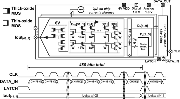
We designed a custom ASIC to drive current to the μLEDs on the optoelectrode. The full circuit schematic is shown in Fig. 5. The chip consists of 48 current digital-to-analog converters (DACs) controlled by an SPI-based serial input, with only 12 current DACs connected to the 12 μLEDs in the present optoelectrode configuration. The DACs drive the μLEDs with up to 1.023 mA current at a 10-bit resolution. The 1 μA current steps provide fine control of emitted optical power while the large output range allows a high optical power option for neural activation in a large tissue volume.
Fig. 5.
LED driver ASIC schematic and input/output signal timing diagram. Modified from [20].
The output currents are simultaneously updated at the rate of 11.72 kHz by feeding 48 10-bit values into an input register which controls the output current level for each DAC channel. The serialized digital input, DATA_IN, is clocked in through the CLK pin and then latched into a decoder at the LATCH signal’s positive edge (shown in Fig. 5, bottom). For every channel, the 10 bit code is split into two halves for the upper thermometer-coded DAC and the lower binary-coded DAC. All final bits are buffered through a register clocked by the LATCH signal to prevent transient logic glitches at the cost of increasing output latency by one LATCH cycle.
Decoded and buffered bits are then fed into an NMOS current steering DAC. The digital signals turn on or off the cascoded current sources controlled by thick-oxide NMOS transistor switches. In order to lower the effective area, the transistor sizing is referenced to 2 μA. The LSB corresponding to a 1 μA current source employs stacked transistors to multiply the effective length by 2, thereby resulting in half its reference current. The code, at which the thermometer/binary DAC split occurs, and the absolute transistor sizing is selected to minimize the chance of non-monotonic output behavior and increase the overall yield. The reference current is generated by an on-chip β-multiplying-style current source.
Since the μLEDs require a voltage compliance well above the allowable supply voltage of the used technology (3.3 V for 0.18 μm), we use a level-shifting current mirror to translate the output voltage while maintaining the same current. The mirror is implemented through a pair of cascoded PMOS transistors which mirror the current coming from the DAC and feed it into the output pads. The supply voltage of 6 V was selected to maintain high linearity by keeping the current mirror in the saturation regime while driving the μLED up to 5 V. Since the high-voltage option of the technology was not used, the output stage has been carefully designed to minimize the effect of large voltage drops across the transistor gates and channels. The thick-oxide long-channel transistors are used, and additional diode-connected transistors are placed between the current mirror and the DAC. Thanks to exponential I-V characteristics of μLEDs, the output transistors do not experience a large voltage drop when driving high currents, extending the lifetime of the circuit. The additional advantage of the long channel design is the increased output impedance which increases the linearity of the current mirror.
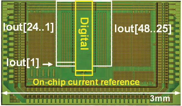
The chip was implemented in 0.18 μm CMOS technology. A chip microphotograph is shown in Fig. 6. Full chip dimensions of 3 mm x 1.5 mm include the active circuitry as well as the power-decoupling capacitors and the wirebonding pads. The active area of the circuit only consumes 1.3 mm2 or 0.272 mm2 per channel.
Fig. 6.
Chip microphotograph of μLED Driver ASIC chip. Modified from [20].
C. Headstage Assembly
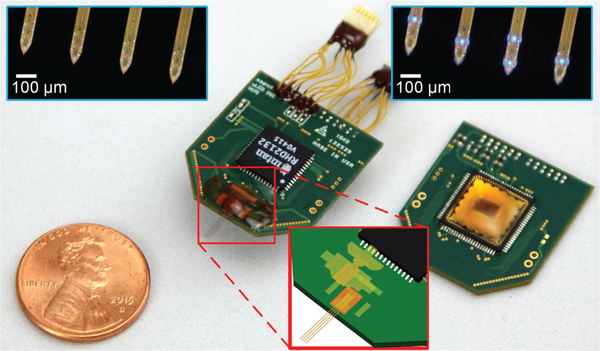
All the fabricated components including an optoelectrode, an LED driver ASIC, and an Intan recording chip (RHD2132) have been assembled on a PCB to form a headstage, as shown in Fig. 7. A single four-metal-layer PCB was used. The two inner layers of the PCB were dedicated as the ground planes for the recording and the stimulation systems. Two ASICs were attached on the opposite sides of the PCB on top of their respective ground planes.
Fig. 7.
Photographs of the assembled headstages. Insets show (top) microphotographies of the tips of the optoelectrodes, and (bottom) the schematic diagram of the polyimide-based flexible cable interposer. The light leakage from the sides of the optoelectrode shank, shown in the top right inset, is an artifact due to the combination of poor light coupling efficiency in the air and high optical output power. Modified from [20].
A polyimide-based flexible cable, similar to that of microflex interconnection [21], was used to provide the electrical connection between the optoelectrode and the PCB. The cable fabricated with a simple two-mask process provides a connection density higher than that acquired from the conventional wire bonding processes. This gives the design freedom by allowing the bonding pads to be placed anywhere on the PCB area. The flexible cable also allows reusability of the headstage because the optoelectrode can be easily dissembled and replaced if needed.
Two ASIC chips and passive components were first reflow-soldered onto the PCB. After that, two 12-pin miniature connectors (Omnetics PZN-12-DD) were attached to the headstage via 2-cm long 36-AWG flexible wires to decouple the tethering force due to long cables between the headstage and the interface control module. The optoelectrode was then attached to the PCB using a flexible polyimide cable as an interposer. After bonding the interposer with the optoelectrode using a ball bonder (K&S 4524D), the optoelectrode-PCB interface was secured with a silicone encapsulant (Dow Corning Sylgard® 184), followed by applying a thin layer of biocompatible epoxy (Epoxy Technology Epo-tek® 353 NDT) for protection.
The dimensions of the assembled headstage are 2.16 cm × 2.38 cm × 0.35 cm. The total mass, including the connectors, is 1.9 g. Since it is generally recognized that the mass of a headstage should not exceed 10% of the weight of an animal for awake and behaving experiments, the low mass as well as the small dimensions of the assembled headstage make it suitable for experiments with awake rodents as well as adult mice [22].
IV. SYSTEM CHARACTERIZATION
The optical stimulation capability of the headstage was first characterized on benchtop. The μLED optoelectrode and the LED driver IC were separately characterized to ensure proper operation of each component. The combined components were then characterized to ensure the performance of the complete assembled headstage.
A. μLED Characterization
The electrical and the optical properties of the fabricated μLED optoelectrode were characterized. The μLED optoelectrode was attached onto a PCB with no active components using the same assembly procedure as in the actual headstage. Electrical connections to the μLEDs were provided with an Omnetics connector.
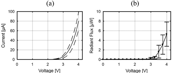
Fig. 8(a) shows the I-V characteristics of μLEDs (n = 5), measured using a sourcemeter (Keithely 2400). The μLEDs have an approximate turn-on voltage of 2 V, and a forward current of approximately 100 μA at 4 V. Fig. 8(b) shows the output radiant optical flux (Φe) as a function of μLED voltage, measured using a voltage source (Agilent E3631A), an integrating sphere (Ocean Optics FOIS-1), and a calibrated spectrometer (Ocean Optics Flame VIS-NIR). The output radiant flux of each μLED was then calculated by integrating the measured spectral flux from λ = 400 nm to 600 nm. The radiant flux from the μLEDs at 4 V bias was measured as 5.3 W, equivalent to irradiance of 33.1 mW/mm2 at the surface of the μLED, which is more than sufficient to excite neurons expressing channelrhodopsin-2 (ChR2) with a threshold irradiance of 1 mW/mm2 [23]. Since we have previously shown that heat dissipation from a 10 × 16 m LED at the tip of a 5-mm long, 70 m wide, and 30 m thick silicon shank during pulsed stimulation induces the temperature increase of the brain tissue less than 1 °C [19], additionalthermal characterization of the assembled headstage was not conducted.
Fig. 8.
The opto-electrical characteristics of μLEDs (n = 7) on the fabricated μLED optoelectrode: (a) I vs. V curves and (b) output radiant optical flux vs. V curves. Dotted lines and the error bars represent one standard deviations from the mean.
B. LED Driver Characterization
The LED driver chip was characterized on a dedicated test PCB while the output currents were monitored using an NI-DAQ interface card. Total of 19 chips were measured.
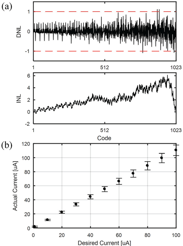
First, nonlinearity was measured to evaluate the precision of current control. Fig. 9(a) shows the differential and integral nonlinearity (DNL and INL) plots from a DAC channel. The average maximum DNL and INL across 19 chips are 1.33 and 6.12, respectively. Since the high DNL values appear mostly at higher codes, the linearity of the DAC is maintained high at lower currents where precision is more necessary. The increase in INL is due to the reduction of output impedance at high μLED currents. The mean and standard deviation of output current is shown in Fig. 9(b). The measured mean output current accuracy from the nominal value is 12.3%, while the average standard deviation is 6.7%. The deviations however do not require additional calibration of the ASIC since the μLED optical output power response should be calibrated after the assembly.
Fig. 9.
DC output current measurements of the fabricated LED driver chip showing (a) differential and integral non-linearity plots, and (b) mean current measurements across 19 dies. Error bars represent one standard deviation from the mean.
The quiescent power consumption of the fabricated chip (excluding I/O power) is approximately 218 μW. Single channel power consumption is a function of the channel current and can be expressed by
| (1) |
where Ich is the desired output current, Vsupply is the output transistor supply voltage (in our current design, Vsupply= 6 V), and γ is a non-ideality factor that should be close to 1. The chip consumes 1.7 mW when driving all 12 μLEDs with a square-pulse current with an amplitude of 100 μA, frequency of 1 Hz, and duty cycle of 10%.
Finally, the stability of current over time was characterized by monitoring the current generated from a channel for an extended period. The chip was programmed to generate a square pulse of 4 Hz with a 50% duty ratio at 100 μA and the amplitude of the generated current was measured. The current from the channel varies less than 1% over one million cycles, which is equivalent to 70-hour long continuous operation.
C. Integrated System Measurements
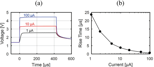
The transient voltage response of μLEDs to different current level pulses was measured to observe the effect of parasitic capacitance and inductance in the interconnection lines. A wire trace on the headstage PCB connecting the on-chip LED driver to the μLED under test was probed and the signal was buffered by a high-speed low-input-capacitance unity-gain amplifier (Analog Devices AD825) and captured by an oscilloscope. Fig. 10(a) shows the measured anode voltage response for 3 current pulses with different magnitudes (1, 10, and 100 μA) while Fig. 10(b) plots the voltage rise times measured for currents between 1 and 100 μA. Low current pulses exhibit longer rise times due to slower charging of the μLED channel’s parasitic shunt capacitance. The rise times, however, are significantly shorter than the biological response (whose detection is sufficient with 20 kHz sampling frequency of the recording chip) and therefore do not affect the in vivo experiment.
Fig. 10.
(a) μLED anode voltage transient response to 3 current pulses of varying amplitudes and (b) plot of changing μLED anode voltage rise time with increasing driving current pulse amplitude.
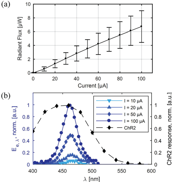
The optical response of the μLEDs on the optoelectrode was characterized using the LED driver IC as the current source to show the effectiveness of LED constant-current control. An integrating sphere and a spectrometer were used to collect spectral response (Φe, ) and the integrated radiant flux (Φe) of each LED at different current levels provided by the LED driver. The average Φe vs. I curve (Fig. 11(a)) shows a nearlinear current-to-radiant flux response with a slope of approximately 68.5 nW/μA in 0 – 100 μA range.
Fig. 11.
The optical characteristics of the μLEDs on the fabricated μLED optoelectrode showing (a) average e vs. I curve (n = 7) and (b) the normalized spectral radiant flux of the μLED at different forward current (with the spectral response of ChR2).
The normalized average spectral radiant flux values from the μLEDs as a function of current are shown in Fig. 11(b). They are superimposed with the plot of the normalized spectral response of channelrhodopsin-2 (ChR2), the most widely used opsin. It can be seen from the graphs that the spectrum of the μLED emission is optimal for activation of ChR2 regardless of the forward current level. The measured peak and the width of the spectrum were approximately 460 nm and 40 nm (FWHM), respectively.
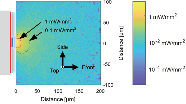
Finally, the profile of the optical power distribution inside the brain tissue was simulated. We built a model of a μLED structure embedded inside brain tissue and performed a ray tracing simulation using Zemax Optic Studio. The refractive index and the absorption coefficient of the μLED structure’s SiO2 passivation layers were measured using an ellipsometer (Woollam M-2000) and used in the model. The values for the refractive indices, the absorption coefficients and the scattering coefficients of the tissue and the other μLED materials were obtained from the literature [24]–[26]. The emission from the μLED was assumed to be monochromatic (λ= 460 nm) for simplicity. The result of simulated irradiance distribution at 100 μA is shown in Fig. 12. A semi-lambertial irradiance profile was obtained in front of the μLED with a few scattered bright and dark spots due to scattering inside the tissue (Henyey-Greenstein Model). The boundary of the volume where irradiance is greater than 1 mW/mm2, known as the threshold irradiance of channelrhodopsin-2, is shown that it is no larger than 20 μm away from the surface of the μLED. The result suggests that the volume of the brain illuminated by the LED can be strictly confined to a small volume near the μLED surface by the precise control of optical power, confirming previous in vivo results obtained using the μLEDs with the same dimensions and configuration [7].
Fig. 12.
Irradiance distribution inside the brain tissue by μLED illumination, on the axial cross-sectional plane with the origin located at the center of the μLED surface. The thickness of the LED, metal, and dielectric layers are not drawn to scale.
Key specifications and measurements of the optoelectrode, the LED driver IC, as well as those of the entire system, are summarized in Table I.
Table I:
SYSTEM SPECIFICATIONS AND PERFORMANCE SUMMARY
| Parameter | Value |
|---|---|
| μLED Optoelectrode | |
| μLED size/wavelength | 10 × 16 μm / 460 nm ± 40 nm |
| μLED output radiant flux | 5.3 μW @ 100 μA |
| Rec. electrode impedance | < 1 MΩ @ 1 kHz (Typ.) |
| LED Drive IC | |
| Current range (resolution) | 0 to 1023 μA (10 bits) |
| LED current update rate | 11.72 kHz |
| Power consumption | (12 ch. @ 100 μA, 10% duty) = 1.7 mW |
| Active Area | 1.3 mm2 (0.272 mm2 per channel) |
| Headstage | |
| # of rec./stim. channels | 32/12 |
| Dimensions | 2.16 cm x 2.38 cm x 0.35 cm |
| Mass | 1.9 g |
| Volume of stimulation | 2660 μm3 @ 100 μA |
V. IN VIVO VALIDATION
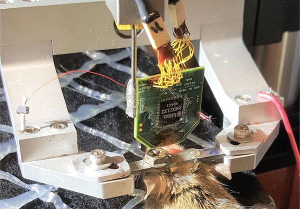
In vivo experiments were conducted to validate the complete system’s capability of simultaneous high-resolution optical stimulation and electrical recording. The animal experiments were conducted at the Buzsaki lab at New York University and strictly followed the protocols approved by the Institutional Animal Care and Use Committee of New York University. A 12-week-old male mouse expressing ChR2 (F1 generation of homozygous CaMKII-Cre crossed with homozygous Ai32 mice, whose expression of ChR2 is restricted to pyramidal neurons) was prepared and anesthetized for acute recordings. The headstage was attached to a stereotaxic frame with a micromanipulator for precise positioning. The setup for the in vivo experiment is shown in Fig. 13.
Fig. 13.
In vivo measurement setup of the headstage. The optoelectrode is implanted into an anesthetized mouse [20].
Measurements were taken from the CA1 region of mouse hippocampus. Localization of the recorded volume was obtained by stereotaxic targeting of known coordinates with help of the micromanipulator. The accurate position of the optoelectrode tips was confirmed by observation of the ripple-patterned oscillations in local field potentials, which is one of the characteristics of the electrophysiological recordings from the hippocampus. After each experimental session, a template matching algorithm was used on the raw recorded data for semi-automated spike sorting followed by manual curation and reclustering of noisy units. All the spike sorting tasks were performed using KlustaKwik.
A. Validation of Optical Induction of Neuronal Activities
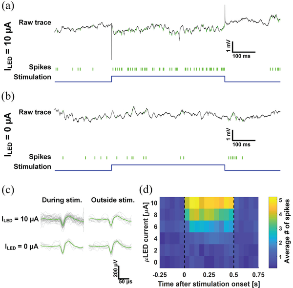
In the first experiment, a single μLED was turned on and the resulting neural responses from the illuminated volume were recorded using nearby electrodes. Current pulses with varying on-time current were generated using the LED driver ASIC. Pulses with forward current of 0, 2, 4, 6, 8, and 10 μA were generated, and the duration of each pulse was 500 ms. Total of 20 pulses with each current level were generated.
Fig. 14(a) and (b) show the raw signals recorded from one of the electrodes around the μLED during stimulation with pulses with 10 μA on-time current and 0 μA (pulse repeat setting was on with zero current setting), respectively. It is clear that the activity of one of the nearby neurons, whose recorded action potentials are indicated in green, is notably increased during the μLED on-time with forward current of 10 μA. The waveform of the filtered action potentials during stimulation on- and off-times remained unchanged (Fig. 14 (c)). We also observed an increase of the neuronal response to the increased light intensity. The peristimulus time histogram as a function of the on-time current (Fig. 14 (d)) shows that the activity of the neuron was notably increased with a forward current greater than 4 μA. This observation is made possible by the high current resolution of the LED driver.
Fig. 14.
In vivo measurements validating the light-induced neuronal activity: raw signals recorded from an electrode as well as the raster plots of spikes from an optically excited neuron during a pulsed stimulation with (a) 10 μA and (b) 0 μA forward currents, (c) waveform of the action potential during the off- and the on-time of the pulse, and (d) peristimulus time histograms of the neuron at different on-time forward currents. Modified from [20].
B. Validation of Selective Local Stimulation Capability
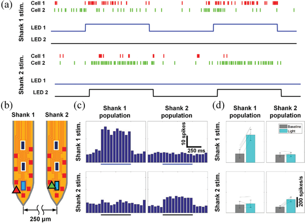
In the second experiment, two μLEDs on the two adjacent shanks were separately turned on. Changes in the activities of the neuronal population near the illuminated region were recorded from the both shanks and the approximate location of the recorded cells were calculated using triangulation.
Raster plots of spikes from two optically excited neurons are shown in Fig. 15 (a). Cell 1 and cell 2 (indicated with red and green triangles, respectively, Fig. 15 (b)) were stimulated using a μLED on shank 1 (LED 1) and a μLED on shank 2 (LED 2), respectively. Stimulation with μLED on one shank did not activate the cell closer to the other shank. The peristimulus time histograms of the neuronal populations around shank 1 and shank 2 during stimulation with μLED 1 and μLED 2 are shown in Fig. 15 (c). The local confinement of the μLED stimulation within a small region surrounding the shank was clearly validated with the change in the activities of the population.
Fig. 15.
In vivo measurements validating selective location neural stimulation: (a) raster plots of spikes from two optically excited neurons responding to different μLEDs, (b) estimated locations of the neurons and the μLEDs, (c) peristimulus time histograms of the neuronal firing around shanks with the respective μLEDs, and (d) averaged (ncycles = 20) baseline and optically induced population spiking rates. Two-sided Wilcoxon’s signed rank test confirms that activities of only the neurons in the vicinity of an activated LED shank are significantly affected by light (for LED 1, pshank 1 = 0.001, pshank 2 = 0.83, for LED 2, pshank 1 = 0.05, pshank 2 = 0.001). Modified from [20].
VI. DISCUSSION
Our system is compared to previously published opto-electrophysiology systems in Table II. The miniature headstage achieves the highest total channel count integration and the highest spatial and LED power resolution within a small form factor and low mass. While the current capabilities are enabled in part by a low-tether-force wired connection, we plan to introduce wireless capability in future work.
Table II:
COMPARISON WITH OTHER OPTO-ELECTROPHYSIOLOGY HEADSTAGE SYSTEMS
| Lee [13] | Kim [6] | Zhao [18] | Nag [14] | Gagnon-Turcotte [16] | Jia [17] | This Work | |
|---|---|---|---|---|---|---|---|
| # stim. ch. | 4 | 4 | 6 | 1/646 | 1 | 4 | 12 |
| # rec .ch | Comm. Sys.1 | Comm. Sys.3 | 4 | 16 | 8 | 2 | 32 |
| Stim. res. | N/A2 | 1-bit (PWM only)4 | 8-bit | 1-bit (PWM only) | 1-bit (PWM only)7 | 8-bit | 10-bit |
| Headstage Mass | - | - | - | 4 g | 4.7 g8 | 5.5 g | 1.9 g |
| Connection | Wired | Wired5 | Wired | Wired5 | Wireless | Wireless | Wired |
32-channel recording performed with Intan Technologies RHD2132 system.
Voltage-control; resolution not reported.
1-channel recording performed with Plexon Omniplex system.
Uncalibrated power through wireless link.
Wireless capability only for stimulation.
64-channel option for LED surface array only.
Current set initially by hardware components.
Including battery
The bidirectional neural interface can be readily used for closed-loop optogenetic experiments with an appropriate algorithm for adaptive control of the stimulation parameters. However, a few improvements can be made on the hardware components of the system to enable the system’s seamless operation for closed-loop experiments.
A. Reduction of Communication Latency
One of the bottlenecks to the ideal closed-loop operation of the system is the long round trip delay in the signal path inside the loop due to the high communication latency between the PC and the interface module. This is mainly due to the slow and inconsistent communication between the PC and the interface PCBs provided by a USB 2.0 connection [27]. It can potentially take up to a few tens of milliseconds for a stimulation command sent from the PC to initiate the desired optical stimuli. While the delay could possibly be insignificant for certain types of experiments, it is suboptimal for the experiments that require the stimulus to be precisely synchronized with fast and stochastic signals such as spiking activity of a specific neuron. Therefore, it would be desirable to reduce the communication latency between the PC and the interface PCB to as low as several hundreds of microseconds.
The communication latency can be significantly reduced by replacing the existing communication links with ones with a higher bandwidth and a shorter latency. One potential candidate is PCI Express, which provides a high data rate of 8 Gb/s with a delay of less than a millisecond [28]. The system could be further modified to utilize a single interface board with the help of the high duplex data bandwidth.
B. Reduction of Stimulation Artifact
Another possible improvement to the system can be made by decreasing the magnitude of the stimulation artifact affecting the recorded electrophysiological signals. The artifact, which shows up at the onset and the offset of the optical stimulation, has relatively short duration (τ < 50 μs) yet high magnitude (500 μV < Vpp < 5 mV). Although it can easily be removed either online with template matching or offline with spike sorting, the artifact can impact the system operation by affecting the quality of the recorded signals and adding extra computational burden.
It is understood that both the electromagnetic interference (EMI) [19] and photovoltaic effect [29] contribute to the stimulation artifact. Whereas the EMI cannot be significantly reduced due to the innate non-ideality of the ground and shielding planes originating from the resistance along the long and narrow shanks of the optoelectrode, the photovoltaic effect can be further reduced by engineering the silicon substrates. SPICE circuit simulation results suggest that the magnitude of the stimulation artifact can be reduced to as low as 50 μV after reducing the photopotential.
VII. CONCLUSION
We have presented a new system architecture for high-precision and high-channel count optical stimulation and electrical recording by integrating an optoelectrode with interfacing ASICs on a single headstage. The system can simultaneously stimulate 12 μLEDs with a spatial resolution as low as 60 μm and record from 32 recording sites with a spatial resolution as low as 20 μm. The constant-current LED driver ASIC can drive up to 48 μLEDs with a 0 to 1.024 mA current range at 10-bit precision and 11.72 kHz update rate. The integrated headstage has a small form factor and a low mass of 1.9 g, enabling its use in behavioral in vivo rodent experiments.
Adam E. Mendrela received the B.S. in electrical and computer engineering from Cornell University, Ithaca, NY, USA, in 2012 and the M.S. in electrical engineering from University of Michigan, Ann Arbor, MI, USA, in 2014 where he is currently pursuing a Ph.D. degree in electrical engineering.
He has interned as an Analog Design Engineer at Mythic, Inc. in 2015. His current research interests include neural interface systems and mixed-signal VLSI circuit design.
Kanghwan Kim received the B.E. degree in electrical engineering from The Cooper Union, New York, NY, USA, in 2013 and the M.S.E. degree in electrical engineering from University of Michigan, Ann Arbor, MI, USA, in 2015. He is currently pursuing the Ph.D. degree in electrical engineering at University of Michigan.
He is developing tools for advanced neuroscience research, including multi-functional neural probes for optogenetics study and recording and stimulation system for real-time closed-loop neuroscience experiments in freely moving animals.
Daniel English received his PhD in neuroscience from Rutgers University, Newark, NJ, USA, in 2012.
He is currently a postdoctoral fellow in the laboratory of Dr. György Buzsáki, in New York University, New York, NY, USA. His research interests center around studying neural circuits, and developing methods to monitor and manipulate them in behaving animals.
Sam McKenzie received his Ph.D. in neuroscience from Boston University, Boston, MA, USA in 2014.
He is currently working as a postdoctoral fellow with Dr. Buzsaki at New York University Medical Center, New York, NY, USA. His work focuses on how plasticity between excitatory and inhibitory neurons affects network dynamics.
John Seymour earned his B.S. with honors in engineering physics from Ohio State University, Columbus, OH, USA, and his M.S. and Ph.D. in biomedical engineering from the University of Michigan, Ann Arbor, MI, USA.
His industry experience includes working at NeuroNexus as a Principal Scientist. He now holds a faculty research position of Assistant Research Scientist in the Department of Electrical Engineering at the University of Michigan, Ann Arbor, MI, developing novel neural interface systems. His research is in the area of advanced neurotechnology with a focus on circuit mapping tools. His research has addressed reduced tissue reactivity and improved optical, electrical, and mechanical performance.
György Buzsáki received his M. D. from University of Pécs, Pécs, Hungary, in 1974 and Ph.D. in neuroscience from Academy of Sciences, Budapest, Hungary in 1984. He is the Biggs Professor of Neuroscience at NYU Langone Health, New York, NY, USA. His main focus is “neural syntax”, i.e., how segmentation of neural information is organized by the numerous brain rhythms to support cognitive functions.
Dr. Buzsáki is among the top 1% most-cited neuroscientists, member of the National Academy of Sciences USA, and the Academiae Europaeae. He sits on the editorial boards of several leading neuroscience journals, including Science and Neuron.
Euisik Yoon received the B.S. and M.S. degrees in electronics engineering from Seoul National University, Seoul, South Korea, in 1982 and 1984, respectively, and the Ph.D. degree in electrical engineering from the University of Michigan, Ann Arbor, MI, USA in 1990.
From 1990 to 1994 he worked for the National Semiconductor Corp. in Santa Clara, CA, where he engaged in researching deep submicron CMOS integration and advanced gate dielectrics. From 1994 to 1996 he was a Member of the Technical Staff at Silicon Graphics Inc. in Mountain View, CA, where he worked on the design of the MIPS microprocessor R4300i and the RCP 3-D graphic coprocessor. He took faculty positions in the Department of Electrical Engineering at Korea Advanced Institute of Science and Technology (KAIST) in Daejon, Korea (1996–2005) and in the Department of Electrical and Computer Engineering at the University of Minnesota, Minneapolis, MN (2005–2008), respectively. During the academic year of 2000–2001, he was a Visiting Faculty at Agilent Laboratory, Palo Alto, CA. In 2008, he joined the Department of Electrical Engineering and Computer Science at the University of Michigan, Ann Arbor, MI, where he is a Professor and the Director of NSF International Program for the Advancement of Neurotechnology (IPAN). He served as the Director of Solid-State Electronics Laboratory (2011–2015) and the Director of Lurie Nanofabrication Facility (2011–2016) at the University of Michigan.
Dr. Yoon has served on various Technical Program Committees including the Microprocesses and Nanotechnology Conference (1998), the International Sensor Conference (2001), the IEEE Asia-Pacific Conference on Advanced System Integrated Circuits (2001–2002), the International Conference on Solid-State Sensors, Actuators and Microsystems (Transducers) (2003, 2005), the IEEE International Electron Device Meeting (2006–2008) and the IEEE International Conference on Micro Electro Mechanical Systems (2006, 2009–2010). He also served on the IEEE International Solid-State Circuit Conference program committee (2003–2007) and was a general chair of International Symposium on Bio Micro & Nanosystems (2005). Currently, he serves as an associate editor for IEEE Solid-State Circuits Letters.
Supplementary Material
Acknowledgments
This work has been supported in part by NIH R21-EB019221 and in part by NSF 1545858 and NSF 1707316 (NeuroNex MINT).
Contributor Information
Adam E. Mendrela, Department of Electrical Engineering and Computer Science at University of Michigan, Ann Arbor, MI 48103, USA. (mendrela@umich.edu, esyoon@umich.edu).
Kanghwan Kim, Department of Electrical Engineering and Computer Science at University of Michigan, Ann Arbor, MI 48103, USA. (mendrela@umich.edu, esyoon@umich.edu).
Daniel English, NYU Neuroscience Institute at New York University, New York City, NY 10016, USA.
Sam McKenzie, NYU Neuroscience Institute at New York University, New York City, NY 10016, USA.
John P. Seymour, Department of Electrical Engineering and Computer Science at University of Michigan, Ann Arbor, MI 48103, USA. (mendrela@umich.edu, esyoon@umich.edu).
György Buzsáki, NYU Neuroscience Institute at New York University, New York City, NY 10016, USA.
Euisik Yoon, Department of Electrical Engineering and Computer Science at University of Michigan, Ann Arbor, MI 48103, USA. (mendrela@umich.edu, esyoon@umich.edu).
REFERENCES
- [1].Boyden ES, Zhang F, Bamberg E, Nagel G, and Deisseroth K, “Millisecond-timescale, genetically targeted optical control of neural activity,” Nat. Neurosci, vol. 8, no. 9, pp. 1263–1268, 2005. [DOI] [PubMed] [Google Scholar]
- [2].Bolus MF, Willats AA, Whitmire CJ, Rozell CJ, and Stanley GB, “Design strategies for dynamic closed-loop optogenetic neurocontrol in vivo,” J. Neural Eng, 2018. [DOI] [PMC free article] [PubMed] [Google Scholar]
- [3].Grosenick L, Marshel JH, and Deisseroth K, “Closed-loop and activity-guided optogenetic control,” Neuron, vol. 86, pp. 106–139, 2015. [DOI] [PMC free article] [PubMed] [Google Scholar]
- [4].Anikeeva P, Andalman AS, Witten I, Warden M, Goshen I, Grosenick L, Gunaydin LA, Frank LM, and Deisseroth K, “Optetrode: A multichannel readout for optogenetic control in freely moving mice,” Nat. Neurosci, vol. 15, no. 1, pp. 163–170, 2012. [DOI] [PMC free article] [PubMed] [Google Scholar]
- [5].Lee J, Ozden I, Song YK, and Nurmikko AV, “Transparent intracortical microprobe array for simultaneous spatiotemporal optical stimulation and multichannel electrical recording,” Nat. Methods, vol. 12, no. 12, pp. 1157–1162, 2015. [DOI] [PubMed] [Google Scholar]
- [6].Kim T-I, McCall JG, Jung YH, Huang X, Siuda ER, Li Y, Song J, Song YM, Pao HA, Kim R-H, Lu C, Lee SD, Song I-S, Shin G, Al-Hasani R, Kim S, Tan MP, Huang Y, Omenetto FG, Rogers JA, and Bruchas MR, “Injectable, Cellular-Scale Optoelectronics with Applications for Wireless Optogenetics,” Science, vol. 340, no. 6129, pp. 211–216, Apr. 2013. [DOI] [PMC free article] [PubMed] [Google Scholar]
- [7].Wu F, Stark E, Ku PC, Wise KD, Buzsáki G, and Yoon E, “Monolithically Integrated μLEDs on Silicon Neural Probes for High-Resolution Optogenetic Studies in Behaving Animals,” Neuron, vol. 88, pp. 1136–1148, 2015. [DOI] [PMC free article] [PubMed] [Google Scholar]
- [8].Scharf R, Tsunematsu T, McAlinden N, Dawson MD, Sakata S, and Mathieson K, “Depth-specific optogenetic control in vivo with a scalable, high-density LED neural probe,” Sci. Rep, vol. 6, Sep. 2016. [DOI] [PMC free article] [PubMed] [Google Scholar]
- [9].Paralikar K, Cong P, Santa W, Dinsmoor D, Hocken B, Munns G, Giftakis J, and Denison T, “An implantable 5mW/channel dual-wavelength optogenetic stimulator for therapeutic neuromodulation research,” in Proc. of 2010 IEEE Int. Solid-State Circuits Conf., 2010, pp. 238–239. [Google Scholar]
- [10].Wentz CT, Bernstein JG, Monahan P, Guerra A, Rodriguez A, and Boyden ES, “A wirelessly powered and controlled device for optical neural control of freely-behaving animals,” J. Neural Eng, vol. 8, 2011. [DOI] [PMC free article] [PubMed] [Google Scholar]
- [11].Rossi MA, Go V, Murphy T, Fu Q, Morizio J, Yin HH, Cohen J, and Hopkins J, “A wirelessly controlled implantable LED system for deep brain optogenetic stimulation,” Front. Integr. Neurosci, vol. 9, 2015. [DOI] [PMC free article] [PubMed] [Google Scholar]
- [12].Zhao H, Soltan A, Maaskant P, Dong N, Sun X, and Degenaar P, “A Scalable Optoelectronic Neural Probe Architecture With Self-Diagnostic Capability,” IEEE Trans. Circuits Syst. I Regul. Pap, pp. 1–12, 2018. [DOI] [PMC free article] [PubMed] [Google Scholar]
- [13].Lee Hyung-Min, Kwon Ki-Yong, Li Wen, and Ghovanloo M, “A wireless implantable switched-capacitor based optogenetic stimulating system,” in Proc. of 2014 36th Annu. Int. Conf. of the IEEE Engineering in Medicine and Biology Society, 2014, pp. 878–881. [DOI] [PMC free article] [PubMed] [Google Scholar]
- [14].Nag S, Lee P, Herikstad R, Sng J, Yen SC, and Thakor NV, “Multi-function optogenetic stimulator and neural amplifier for wirelessly controlled neural interface,” in Proc. of IEEE Biomedical Circuits and Systems Conf., 2015. [Google Scholar]
- [15].Ameli R, Mirbozorgi A, Neron JL, Lechasseur Y, and Gosselin B, “A wireless and batteryless neural headstage with optical stimulation and electrophysiological recording,” in Proc. of 2013 Annu. Int. Conf. of the IEEE Engineering in Medicine and Biology Society, 2013, pp. 5662–5665. [DOI] [PubMed] [Google Scholar]
- [16].Gagnon-Turcotte G, LeChasseur Y, Bories C, Messaddeq Y, De Koninck Y, and Gosselin B, “A Wireless Headstage for Combined Optogenetics and Multichannel Electrophysiological Recording,” IEEE Trans. Biomed. Circuits Syst, vol. 11, no. 1, pp. 1–14, 2016. [DOI] [PubMed] [Google Scholar]
- [17].Jia Y, Khan W, Lee B, Fan B, Guo Y, Madi F, Weber AJ, Li W, and Ghovanloo M, “A wireless opto-electro neural interface for experiments with small freely-behaving animals,” in Proc. of IEEE Biomedical Circuits and Systems Conference, 2017. [DOI] [PMC free article] [PubMed] [Google Scholar]
- [18].Zhao H, Dehkhoda F, Ramezani R, Sokolov D, Degenaar P, Liu Y, and Constandinou T, “A CMOS-based neural implantable optrode for optogenetic stimulation and electrical recording,” in Proc. of IEEE Biomedical Circuits and Systems Conference, 2015. [Google Scholar]
- [19].Kim K, English D, Mckenzie S, Wu F, Stark E, Seymour J, Ku P, Wise K, Buzsaki G, and Yoon E, “GaN-on-Si μLED optoelectrodes for high-spatiotemporal-accuracy optogenetics in freely behaving animals,” in Proc. of IEEE International Electron Devices Meeting, 2016, pp. 643– 646. [Google Scholar]
- [20].Mendrela AE, Kim K, English D, Mckenzie S, Seymour J, Buzsáki G, and Yoon E, “A Miniature Headstage for High Resolution Closed- Loop Optogenetics,” in Proc. of IEEE Biomedical Circuits and Systems Conference, 2017. [DOI] [PMC free article] [PubMed] [Google Scholar]
- [21].Stieglitz T, Beutel H, and Meyer JU, “‘Microflex’ - A new assembling technique for interconnects,” J. Intell. Mater. Syst. Struct, vol. 11, no. 6, pp. 417–425, 2000. [Google Scholar]
- [22].Voigts J, Siegle JH, Pritchett DL, and Moore CI, “The flexDrive: an ultra-light implant for optical control and highly parallel chronic recording of neuronal ensembles in freely moving mice,” Front. Syst. Neurosci, vol. 7, no. May, pp. 1–9, 2013. [DOI] [PMC free article] [PubMed] [Google Scholar]
- [23].Stark E, Koos T, and Buzsáki G, “Diode probes for spatiotemporal optical control of multiple neurons in freely moving animals,” J. Neurophysiol, vol. 108, no. 1, pp. 349–363, Jul. 2012. [DOI] [PMC free article] [PubMed] [Google Scholar]
- [24].Liu Z, Wang K, Luo X, and Liu S, “Precise optical modeling of blue light-emitting diodes by Monte Carlo ray-tracing.,” Opt. Express, vol. 18, no. 9, pp. 9398–9412, 2010. [DOI] [PubMed] [Google Scholar]
- [25].Johansson JD, “Spectroscopic method for determination of the absorption coefficient in brain tissue,” J. Biomed. Opt, vol. 15, no. 5, 2010. [DOI] [PubMed] [Google Scholar]
- [26].Stujenske JM, Spellman T, and Gordon JA, “Modeling the Spatiotemporal Dynamics of Light and Heat Propagation for InVivo Optogenetics,” Cell Rep, vol. 12, no. 3, pp. 525–534, 2015. [DOI] [PMC free article] [PubMed] [Google Scholar]
- [27].Siegle JH, Hale GJ, Newman JP, and Voigts J, “Neural ensemble communities: open-source approaches to hardware for large-scale electrophysiology,” Curr. Opin. Neurobiol, vol. 32, pp. 53–59, 2015. [DOI] [PMC free article] [PubMed] [Google Scholar]
- [28].Newman J, Zhang J, Voigts J, Cuevas Lopez A, and Wilson MA, “An open-source PCIe based electrophysiology system for high data rate, low-latency closed-loop experiments,” in Society for Neuroscience, 2017. [Google Scholar]
- [29].Wise KD, Angell JB, and Starr A, “An Integrated-Circuit Approach to Extracellular Microelectrodes,” IEEE Trans. Biomed. Eng, vol. BME-17, no. 3, pp. 238–247, 1970. [DOI] [PubMed] [Google Scholar]
Associated Data
This section collects any data citations, data availability statements, or supplementary materials included in this article.


