Abstract
Recording neural activity in live animals in vivo with minimal tissue damage is one of the major barriers to understanding the nervous system. This paper presents the technology for a tetherless opto-electronic neural interface based on 180 nm CMOS circuits, heterogeneously integrated with an AlGaAs diode that functions as both a photovoltaic and light emitting diode. These microscale opto-electrically transduced electrodes (MOTEs) are powered by, and communicate through an optical interface, simultaneously enabling high temporal-resolution electrical measurements without a tether or a bulky RF coil. The MOTE presented here is 250 μm × 57 μm, consumes 1 of electrical power, and is capable of capturing and encoding neural signals before transmitting the encoded signals. The measured noise floor is as low as 15 μVrms at a 15 KHz bandwidth.
Keywords: Neural interface, neurophysiology, PVLED, tetherless neural recording
I. Introduction
ELUCIDATING how the brain works is a grand scientific challenge and will help us better understand neurological diseases such as Alzheimer’s and Parkinson’s [1]. Decades of research have provided us with a sound understanding of how neurons function, individually or in small numbers. Meanwhile, functional magnetic resonance imaging (fMRI) provides knowledge of brain activities over large volumes at second-to-minute time scales [2], Naturally, there is a strong interest in bridging this gap in understanding by chronically recording from large populations of neurons in awake, behaving animals [3].
While large-scale parallel recording of neural activity through densely packed planar micro-electrode arrays (MEAs) has revolutionized the study of some neural circuits [4, 5], such systems are limited to in vitro studies and are too large to be inserted into intact tissue. For in vivo studies, multi-electrode probe shanks [6, 7, 8] have shown promise. However, such techniques typically require electrodes to be tethered to the outside world directly via a wire, or indirectly via an RF coil [9, 10, 11], which is much larger than the electrodes themselves and must reside outside the brain. Tethered implants, however, result in residual motion between neurons and electrodes as the brain moves, limiting recording stability and exacerbating gliosis [12], Furthermore, such tools stand in the way of recording from peripheral nerves in moving animals, in particular in smaller organisms such as zebra fish or fruit flies.
Recently, there have been increasing efforts to build microscale untethered neural implants: the main challenge in such cases is delivering power and communicating data wirelessly. For example, microscale RF systems have been designed with integrated coils, but still require a cross section of 200 μm × 200 μm to capture enough RF magnetic flux [13].
Ultrasonic (US) has gained interest as a modality for wireless power transfer and communication for neural implants [14,15], While US provides better focusing of energy than RF, the transduction between the US signals in tissue and the voltage from piezoelectric material is not efficient, especially as the piezoelectric transducers fall below the US wavelength (~100s |am for medical US frequencies) [16], Furthermore, the US power and communications require rectification of high frequency, further degrading efficiency.
Optical imaging techniques, on the other hand, based on voltage or calcium sensitive dyes and/or proteins allow noninvasive imaging of larger numbers of neurons’ activities [17, 18], But such techniques are often limited to subsets of neurons in any given organism, are impeded by scattering of the excitation light and emitted fluorescence, and are limited to low temporal resolution [19], Thus, there is a need for small, tetherless systems to record electrical signals while minimally displacing tissue, and, ideally, minimally obstructing optical signals for simultaneous electrical and optical recording.
In this work, we attempt to combine the merits of optical and electronic modalities. We present a micro-scale opto-electronically transduced electrode (MOTE) for an untethered electrode unit, powered by, and communicating through a microscale optical interface, similar to that recently presented in [20], but with enhancements in size and performance - a factor of two reduction in area and a factor of three reduction in noise floor despite using the same technology nodes (180 nm CMOS). Light provides MOTEs with a means for deep, tetherless penetration into a brain because light in the brain (infrared in particular) is mostly scattered rather than absorbed by brain tissue [21], Although conventional imaging based on focusing optics is hindered by such scattering, simple power harvesting and communications is less sensitive to (and may even be helped by) heavy scattering of light. On the other hand, electrical recording can provide fast, high temporal-fidelity recording of neural activity without relying on biological modifications or secondary chemical reactions.
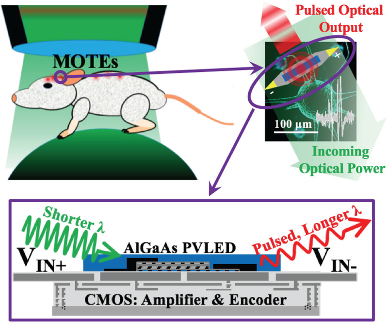
Fig. 1 shows a simplified system overview of the MOTE where the unit is optically powered through a heterogeneously integrated AlGaAs photo-voltaic (PV) which also intermittently acts as a light emitting diode (LED) [22, 23] to optically uplink the measured neural signals. Once inserted into a tissue, such MOTEs should be able to provide tetherless neural recording as illustrated in Fig. 1 under conditions similar to, (but less stringent than) those used for optical imaging. Because of its tetherless nature and micro-scale dimensions, there is an array of applications, in addition to recording in the brain, where MOTEs could prove themselves useful such as spinal cord and peripheral nervous system monitoring.
Fig. 1.
Overview of MOTE and its envisioned implementation. Ideally, MOTEs can be implanted into a subject without hindering subject’s freedom of motion. Because a MOTE is optically powered, and transmits the measured neural signals optically as well, the subject needs to be optically accessible, similar to in imaging. In this figure, a mouse on a trackball is shown as an example where the mouse can move almost freely while overhanging optics provide the power as well as signal detection.
The rest of the paper is organized as follows: we first derive basic limitations and requirements on a MOTE design and describe our system approach - for simplicity, we will assume transcranial environment similar to that used for live-brain imaging through cranial windows. Based on this we describe the critical circuit designs in the MOTE, followed by measured results. We also describe the physical integration of the MOTE, compare to other approaches and discuss further work to be done.
II. Feasibility and Design Specifications
Before discussing the details of our present MOTE design, we first discuss the critical limits on MOTE performance to define design boundaries for MOTE.
A. Safety Limits on Light Intensity in the Brain
A MOTE is powered optically through a PV. While the intrinsic, open circuit voltage of the PV dictates the supply voltage (Vdd), the available supply current is dependent on the light intensity on the PV. Although increasing the light intensity makes the circuit design easier by providing proportionally larger supply current, there are safety limits on light intensity in the brain, mainly due to heating concerns. The reported onset of damage for near IR is 250–300 mW over 1 mm2 for 20 minutes of continuous exposure, corresponding to a 5 °C increase in the illuminated region of the brain [24], For this work, we will assume the exposure of ~100 mW over 1 mm2 unless stated otherwise, corresponding to less than 2 °C of heating (and this canbe less if duty-cycled [24]).
The maximum depth at which MOTEs can be optically powered enough to function is set by this above limit, and the intensity attenuation in the brain:
| (1) |
which is a function of depth d and attenuation length (d0), where the exponential term accounts for diffusive absorption and scattering and the latter d−2 term describes the spherical spread of photons (the incident power is assumed to be a point source for simplicity). Multiple attenuation lengths have been reported, between 2 and 4 mm depending on brain blood content, etc. [25, 26], and we have used d0 = 2.8 mm in following calculations.
For the 50 μm × 100 μm AlGaAs diode implemented in this work (Voc ~ 1 V), ~1.65 μW of optical energy will be available at 6 mm deep into the brain (the full thickness of a mouse brain) versus −20 μW at d = 3 mm and ~500 μW at the surface (for 100 mW across 1 mm2). For the design presented herein, we use 1 μW of electrical power (Vdd = 1 V) which, accounting for our current PV efficiency of 9 %, should allow to function at more than 3 mm of depth. An obvious goal going forward is to improve the PV efficiency (near 30% is possible and widely demonstrated for GaAs [27]) and to reduce the MOTE power consumption to allow it to function down to 6 mm. It should be also noted that while the absorption length is ~2.8 mm, the scattering length in brain tissue is much less (scattering coefficient, μs, is on the order of 30–100 μm [28]) such that MOTEs deeper in tissue can be expected to receive scattered illumination from all sides, and so are relatively insensitive to their orientation relative to injected light.
B. Functional Requirements
MOTEs have two power-critical functions that set trade-offs between direct current (DC) power consumed and performance: 1) the MOTE needs to measure and to amplify differential electrical signals between two exposed platinum electrodes (Vin+ and Vin−) with sufficiently low noise to detect spikes and local field potentials (LFPs); and 2) a MOTE needs to emit sufficiently strong optical pulses to be detected and decoded during data uplink.
In order to minimize the effect of variable attenuation on the optical data transfer, we have implemented pulse-position modulation (PPM) scheme, where the time elapsed between pulses encodes the measured voltage (as compared to encoding based on signal amplitude). PPM encoding is also the most photon-efficient method for carrying information, and so is common in photon-starved applications such as satellite communications [29].
The PVLED must switch for ~1 microsecond from PV to LED when sending a light pulse, so the power harvesting will be interrupted briefly to generate the PPM light pulse. The pulse is provided by charging metal-oxide-semiconductor (MOS) capacitors slowly from the PV before discharging them quickly through the LED, emitting a short pulse whose peak power is significantly higher than the average power absorbed by the PV. Decoupling MOS capacitors, meanwhile, hold the supply rail stable during the LED emission.
C. Signal Requirements
1). Measurement noise and gain
For transistor circuits in subthreshold operation, input referred noise is limited by Boltzmann statistics. At the biologically relevant temperature of 310 K, the input referred noise of an amplifier can be described in terms of bandwidth (BW), bias current (Ibias) [30] and amplifier noise efficiency factor (NEF [31]) to be
| (2) |
A target input-referred noise floor of 10 μVrms and BW of 10 KHz, is acceptable for many neural applications [9], The required Ibias, then, has to be larger than 20 nA (for NEF = 1). Realistically, simple amplifiers built from MOS transistors have a NEF of 3–4, implying the bias current (Ibias) ~300 nA, though recent, more complex designs have shown somewhatlowerNEFs [32, 33, 34].
This amplifier also needs to achieve a sufficient gain to ensure the noise (and so Ibias) can be relaxed for subsequent stages. Yet, the drain-source bias voltage (Vbias) of a transistor limits its gain [35] to
| (3) |
For a target gain Av = 30 V/V, this requires Vbias > 90 mV, and therefore Vdd >180 mV (assuming an active load). Again, a margin of > 2× (Vdd > 400 mV) is needed in practice.
2). Uplink
Assuming the same attenuation as in (1), and assuming a 10 mm2 photon capture area at the brain surface, we can expect about 0.05 % of the photons emitted by an uplinking MOTE at 6 mm deep in the brain to reach the detector. Modern detectors, in particular those used in multi-photon microscopy (MPM) can resolve as few as 10 photons in a brief time window [36], though filters and other components in the light path tend to pass only about 10% of incident photons. Thus, the MOTE’s LED needs to emit at least 200,000 photons, which for a 10% efficient LED with a turn on voltage of ~1 V corresponds to 3.2 pJ. The required average power will be the single pulse energy times the pulse rate which we designed to be up to ~40,000 pulses per second (for a 20 KHz sample rate), leading to the power consumption of~130 nW.
3). Other Circuitry
As shown above, ~500 nW with Vdd = 1 V is needed for the amplifier and pulse generator. Additional power is used for other functions such as stable biasing and encoding, whose power consumption is less clearly linked to system performance, but must be optimized against physical size and reliability.
D. MOTE ScalingforMinimum Tissue Damage
Prior work has shown that traditional metal electrodes with ~80 μm diameters record successfully, but cause damage to the vasculature and trigger significant gliosis, whereas carbon-fiber electrodes with diameters of ~10 μm appear to be all but benign [37]. Given the area requirements posed by PV, capacitance, and amplifier, scaling down to a 10 μm cross section presents an extremely challenging long-term goal. For the work described herein, we aim for a volume of 60 μm × 250 μm × 50 μm implemented in 180 nm CMOS.
III. CMOS Circuit Blocks for MOTEs
A. System Overview
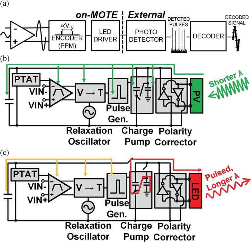
The MOTE system can be broken into two parts. The first part is the CMOS circuitry integrated with AlGaAs PVLED, and the second part is the external measurement system with photodetector and decoder. Here we primarily focus on the MOTE itself. Fig. 2(a) describes the signal flow going through the CMOS circuitry (on-MOTE) and the external setup for the uplinked signal to be detected and decoded. Fig. 2(b) and Fig. 2(c) illustrate the operation of MOTE circuitry during PV and LED modes of operations in block diagrams, respectively.
Fig. 2.
System overview of a MOTE [20]: (a) an exemplary signal flow through the CMOS circuitry followed by the external detector and decoder; (b) a MOTE block diagram in PV mode; (c) a MOTE block diagram in LED mode.
In brief, when first illuminated, the MOTE (in its PV mode) goes through a start-up sequence that lasts about 4 clock cycles (~100 μs) described below, after which it enters normal operation. A differential band-pass amplifier continuously amplifies the differential voltage across a pair of input electrodes and generates a proportional current. A relaxation oscillator triggers every ~60 μs switching to LED mode for ~1 μs to generate a current pulse to the LED. Between 15 μs and 45 μs later a second pulse is generated whose timing (respect to the first pulse) is proportional to the output of the amplifier. The guard-time of 15 μs is maintained between the pulses to allow the LED driver time to recharge between the pulses.
1). Constant Bias Current Generator (PTAT)
In order to provide a stable current supply over varying light intensities, we use a simple PTAT circuit and exploit the relatively stable temperature in vivo. This constant current in turn stabilizes the oscillator frequency, encoder gain, LED driver charging rate, etc. The primary trade off in the bias design for a MOTE is between power consumption, accuracy and physical size:
| (4) |
where η is the non-ideality constant, VT is the thermal voltage kT/q ~ 26mV, N is the device size ratio, and Rref is the reference resistance. The accuracy improves with increasing Vref = ηVTln(N) compared to VTH mismatch, and the current is reduced by increasing Rref, which makes the physical size of the resistor large. In this design, we have compromised by setting Rref ~ 1 MΩ, and Vref ~ 50 mV to minimize the current while keeping Ibias variation to ±20 % across mismatch and process.
2). Amplifier
The amplifier uses half the power available (500 nW out of 1 μW) to provide a desired noise floor close to 10 μVrms. It is inverter-based [38, 39] to provide additional gm for the same current but lower noise than our earlier work [20], The amplifier sets the gain, noise and bandwidth of the MOTE.
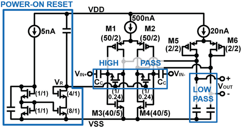
Filtering is crucial as the PPM encoding employed MOTE acts as a type of sampling, which can alias out-of-band noise from the amplifier if not low-pass filtered. Fig. 3 shows a simplified schematic for the amplifier used. The inverter-based differential pair (Ml & M2 and M3 & M4), loaded by M5 & M6 provides a voltage gain of ~30 dB. The metal-insulator-metal (MIM)-based input capacitors (CC) and feedback biasing transistors (which act as large resistors when Vr is in its normal state) are designed to provide a high-pass comer below 10 Hz, preventing the amplifier from saturating due to DC offsets or drift on the electrodes. Shunting MOS capacitors provide a low-pass comer at around 10 KHz for anti-aliasing.
Fig. 3.
Simplified schematic of complementary, invertor-based band-passing amplifier employed in MOTE. The amplifier is largely consisting of gain stage, high pass, low pass, and power-on reset. Numbers in parenthesis denote the transistor sizing width/length in microns.
Though the biasing feedback pseudo resistors deliver a low frequency high-pass comer with little area overhead, this also causes a long settling time (~100 ms for the highpass comer at 10 Hz) in the amplifier’s bias, preventing rapid wake-up of the MOTE, which is desirable in cases of duty-cycled illumination. Therefore, we have also implemented a power-on reset to briefly set the pseudo resistance value low (‘turning on’ the transistors by doubling the Vr) shortly after the PTAT turns on, allowing rapid bias settling on the order of milliseconds. This allows the input amplifier to operate with a low high-pass comer without having to wait a similar time constant to wake up.
Lastly, the flicker noise dictates the minimum size for Ml, M2, M3, and M4, which could be reduced at more advanced technology nodes [40].
3). Encoder (PPM) and Oscillator
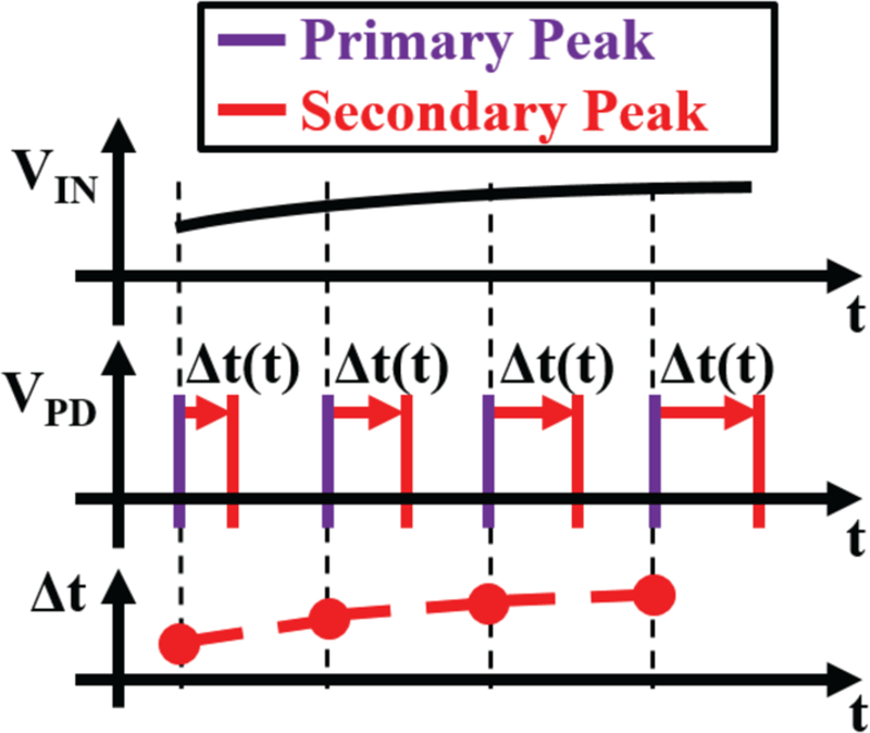
An encoder with a relaxation oscillator follows the amplifier, to convert the amplified differential voltage signal into pulses that are fed to the LED driver. The time between pulses encodes the amplifier’s output voltage. In detail, the pulses come in pairs, where the primary pulses are supplied by the relaxation oscillator, and the secondary pulses are time-shifted (in respect to the primary pulses) by the voltage.
Fig. 4 depicts an overview of the PPM encoding in MOTE: a monotonically increasing input voltage is reflected in timed light pulses which can be decoded from the spacing between the primary and the secondary pulses.
Fig. 4.
Example of PPM encoding employed in MOTE where Vpd and Δt denote photodetector output and pulse spacing (between the primary and secondary), respectively [20].
Fig. 5 illustrates the encoder circuit used to realize the timing in Fig. 4. Each clock (relaxation oscillator) cycle resets Venc, while the amplifier’s output voltages (Vin in Fig. 5) are converted into current to discharge the charge stored on Venc. Thus, the time to discharge decreases as the input voltage increases. Venc is passed through current starved invertors to generate irregular duty cycled square-wave, Vout, whose edges are later converted into pulses.
Fig. 5.
Encoder circuit of MOTE including relaxation oscillation with timing diagram. The voltage output from the amplifier (VIN) determines the current outflow from the capacitor, hence dictating the slope of VENC decay relative to that of the oscillator VOSC. The slope is then used to create irregular duty cycle VOUT to generate current pulses whose spacing tracks the VIN.
The relaxation oscillator and the encoder use similar structures. Ratio-ed current sources and MOS capacitors ensure the oscillation period and encoding track across process variation with a constant ratio, with Vosc discharging more slowly than Venc to ensure Venc always passes the threshold before Vosc.
4). LEDD river
Vout from the encoder circuit (Fig. 5) must be re-coded as pulses and fed into a charge pump circuit to generate corresponding current pulses, which through the PVLED, become light pulses.
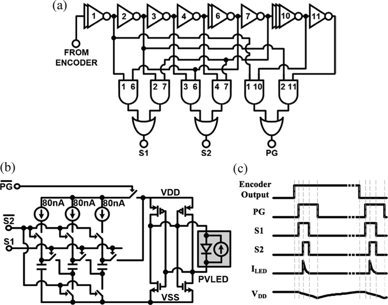
Fig. 6 shows a simplified schematic of the pulse generator, charge pump and associated timing diagram. A set of switched MOS capacitors constitutes the charge pump, and the 80 nA constant current sources ensure that the Vdd is not overloaded during a charge cycle (PV mode) but recharges in ~15 μs. In LED mode, the capacitors are connected in series to discharge onto the PVLED, generating a brief light pulse. The cross-coupled invertors that interface the PVLED acts as a sign corrector for ease of integration - it would not matter which orientation a PVLED is connected onto the CMOS chips supply pads.
Fig. 6.
LED-driver circuits: (a) pulse generation circuitry: generates three pulses using a current-starved inverter chain and current-limited logic: a ~1 μs power-gating pulse (PG) to isolate the PVLED from VDD and the other two pulses (SI and S2) that reconfigure the charge pump from parallel to series to drive the LED; (b) charge pump and PVLED interface circuitry: during the normal, charging operation, MOS capacitors are connected to VSS and charged in parallel by 80 nA current sources, which are supplied from VDD that is connected to the positive node of the PVLED through the sign corrector circuit. During the LED pulsing mode, PG disconnects VDD to connect MOS capacitors, in series, to the LED; (c) timing diagram of the pre-described pulses, resulting current pulses, and VDD ripple.
Each time a current pulse is sent to the LED, three steps must happen in series: (1) the PVLED must be disconnected from the Vdd rail of the MOTE to prevent charge from being directed back into the MOTE instead of to the LED. Vdd is held stable through a bank of decoupling MOS capacitors. (2) The MOS capacitors in the charge pump must be disconnected from their charging rails so that they are no longer in parallel, and (3) the charge pump capacitors must be connected in series, and so discharged through the PVLED. These different events must occur in the proper order (see the timing diagram in Fig. 6), and with enough time between them to prevent unwanted discharge paths in the charge pump. This timing was generated through a 12-stage delay line of starved inverters, driving NMOS logic gates with fixed 10nA pull-ups. All logic gates are current-starved to prevent crow-bar current caused by the relatively slow edges from the encoder and the delay line.
Because Vdd is disconnected during each transmitted pulse, a MOS capacitor is used to stabilize the supply and minimize ripple to about 50 mVpp. This ripple could couple into the measurement path due to device mismatch. However, the ripple is outside of the amplifier’s bandwidth, and is fully correlated with the sampling of the system that such coupling will mostly be suppressed, and/or manifest as fixed DC offset due to aliasing.
5). Startup Circuits
One potential failure mode for this design comes from interactions between bias state, pulse timing, and Vdd. This can be an issue during startup after illumination first turns on, but before bias states are fully settled. In particular, if the pulse controlling the supply switch (PG in Fig. 6) between Vdd and the PVLED is too long (due to low bias currents slowing the delay line), then Vdd can discharge too much during the LED pulse that bias current is impacted, slowing the pulse, and putting the MOTE in an unwanted nonfunctional state. This and other such failure modes are avoided by a start-up sequence that first resets the PTAT to avoid its low-current metastable state, then waits 3 clock cycles before activating the pulse generation circuitry, allowing sufficient time for all biases to settle.
6). Area and Power Breakdown
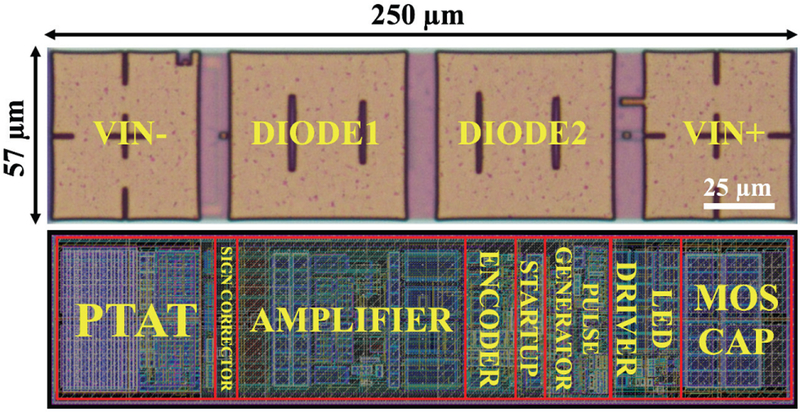
Fig. 7 shows the die micrograph and layout of the CMOS part of the MOTE with major circuit blocks annotated. Instead of denoting as anode and cathode, the PVLED interface is marked with diodel and diode2 to emphasize the fact that built-in sign corrector can allow a MOTE to function irrespective of the PVLED (to be transferred onto the CMOS) orientation.
Fig. 7.
Die micrograph of the 180 nm CMOS die (top) and the layout (bottom) with underlying circuitries annotated.
A rough breakdown of the ~1 ^W power consumption in the MOTE during LED driver recharging is: 50 % in the amplifier, 25 % in the LED driver, 15 % in the oscillator and encoder, and 10%in the PTAT.
B. Measurement
1). Measurement Setup
In order to characterize the CMOS circuitry, which was fabricated in a standard 180 nm process, we first wire-bonded (Westbond 7400A) the CMOS die with an AlGaAs diode (PVLED) to assemble a MOTE and bonded the differential input electrodes to a printed circuit board (PCB). The measurement setup is a standard fluorescent microscope (ZEISS Axio Examiner.Dl) with slight modifications.
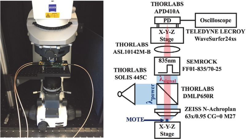
Fig. 8 provides a picture of the measurement setup along with an explanatory schematic. To be compatible with our microscope, a shorter wavelength light (λ= 445 nm, colored blue in Fig. 8) was projected onto the MOTE through a dichroic mirror. Because of the dichroic mirror and subsequent optical band-pass filter, the shorter wavelength light does not reach the photodetector. We have designed the PVLED to emit around λ = 835 nm, which the dichroic mirror passes to an aspheric lens and finally the photodetector (red-colored optical path in Fig. 8). The photodetector output is then read through an oscilloscope and is decoded using MATLAB.
Fig. 8.
Measurement setup used for MOTE characterization [20].
2). Measurement Results
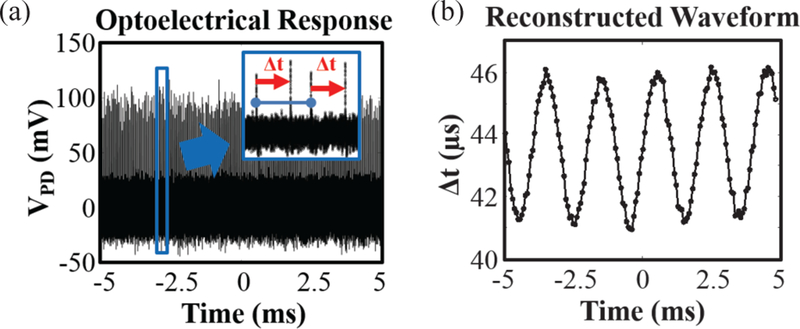
A typical photodetector output contains a train of irregular pulses from which the input signal could be retrieved. Fig. 9(a) shows such pulse trains where the zoom-in inset shows primary peaks (blue) and secondary peaks (tips of the red arrows). The length of the red arrows, i.e., the spacing between the primary and secondary peaks contains the information on the input voltage. With that observation, one can reconstruct the input signal as shown in Fig. 9(b) where its total harmonic distortion (THD) was −16.5 dBc for the first five harmonics. The distortion is likely dominated by the non-linearity in the amplifier as well as PPM encoding.
Fig. 9.
(a) Opto-electrical pulse train of MOTE in response to VIN = 177 μVRMS at 500 Hz: once zoomed-in, irregular pulse trains are observed; (b) based on the temporal spacing between the peaks shown in (a), denoted with red arrows, the original waveform can be faithfully reconstructed.
For this work, we have used simple thresholding for locating peaks, which inherently requires a minimum SNR of ~20 dB in the optical readout. While more sophisticated algorithms for peak detection can allow SNR < 20 dB to be decoded, with our current decoding scheme, we have observed as little as 50 mW/mm2 was sufficient to activate these first-generation MOTEs. Employing detectors from a MPM setup, which can achieve as few as 10 photons sensitivity [41, 42], compared to our current photodetector’s noise floor of a few hundred photons [43] would further enhance our uplink SNR by more than an order of magnitude, and the minimum power required as a result.
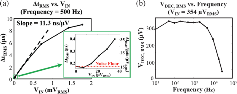
As the MOTE provides voltage-to-time transduction, the gain of the system can be defined in units of time/voltage. Fig. 10(a) shows the gain of the proposed system from electrode input to decoded output optical pulses. The transduction gain is about 11.3 ns/μV and saturates at around 1.5 mVRMS, enough to accommodate most neural signals of interest [44], The input referred noise floor was 15 μVrms as shown in the inset of Fig. 10(a) which of right axis denotes tRMs divided by the transduction gain (the linear slope in the main figure).
Fig. 10.
Characteristic functions of a MOTE: (a) transduction gain (Δtrms vs. input voltage) plot with a zoomed-in inset to show the noise floor; (b) transfer function to show the high-pass and low-pass comers of MOTE. The y-axis denotes the decoded input voltage by observing the PPM output and dividing by the gain shown in (a).
Fig. 10(b) illustrates the transfer function. The low-pass comer is about 15 kHz, close to designed for. While the high-pass comer of the transfer function shown is lower than expected, multiple chips measurement showed that the highpass comers ranged between 5 Hz and 10 Hz, close to the design target. It is suspected that model inaccuracy/process variation have led to lower steady-state (as to initial, startup state) Vr than designed for, leading to higher resistance than desired.
As mentioned earlier, it is important for the MOTE to wake up within a reasonable fast time window (<10 ms) as duty-cycled illumination can be desirable to minimize the increase in temperature, hence avoiding biological damage at high power illumination [24].
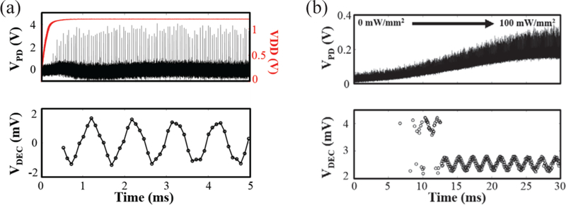
Fig. 11 confirms that the MOTE can wake up on a milli-second time scale. Fig. 11(a) shows an electrical wakeup through an external voltage bias which clearly shows a sub-ms wakeup as intended. Fig. 11(b) shows an optical wakeup, where the illumination ramps-up over ~10 ms, even here it is clear that MOTE starts to opto-electronically transduce as soon as the power is supplied. The light pulses at the beginning of the measurement (i.e., <15 ms) in the optical wakeup are not detected efficiently enough to provide SNR > 20 dB, therefore it can be seen that the simple threshold decoding scheme breaks down. Nonetheless, from the electrical wakeup data, it is highly likely that we will be able to observe optical wakeup on time scales similar to the electrical wakeup in Fig 11(a) using a better optical apparatus.
Fig. 11.
Wake-up test on MOTE to confirm the wake-up in milli-second time scale: (a) electrical wakeup when input signal is VIN = 2 mVPP (708 μVRMS) @ 1 KHz [20]; (b) optical wakeup VIN = 500 μVPP (177 μVRMS) @ 500 Hz. Upper plots show photodetector output whereas the bottom plots showthe decoded, reconstructed signal.
Furthermore, the switching of our light source is inherently slower than the switching of voltage source, and slow switching can affect the startup time for MOTE. While the wakeup time of several milliseconds is not desirable, such wakeup time should not affect the utility of a MOTE in continuous exposure mode. Even in a pulse operation (to utilize higher light intensity), though the first several milliseconds of information (in addition to the off-period of the duty cycle) will be lost, given that even duty-cycled illumination employs light pulses of 10 seconds [24], 10’s of ms turn on time will not lead to significant loss of data. Nonetheless, more work is needed on techniques to better wake up the MOTE during slow optical turn-on.
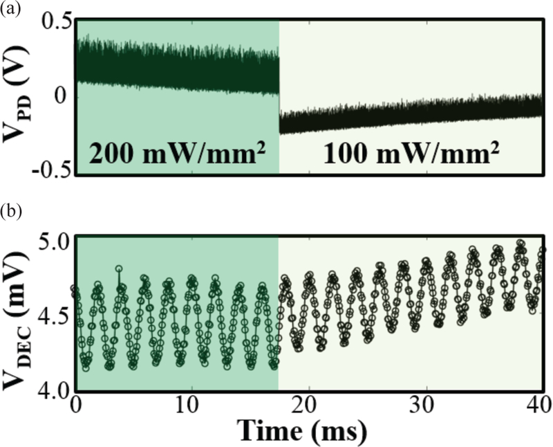
It is also imperative that the MOTE to function under varying light levels (due to shifting focus during imaging, for example), which was the main rational behind the adaptation of the PTAT. Fig. 12 demonstrates that the MOTE can indeed perform consistently even under varying light levels. The input sinusoid was easily decoded using simple DC subtraction followed by thresholding. The two light levels have been chosen as the 100 mW/mm2 is within the safety limit while 200 mW/mm2 is above for continuous exposure [24], while the pulsing between the two levels, depending on its duty cycle, could be deemed safe.
Fig. 12.
MOTE characterization under varying light level: (a) the photodetector output; (b) the decoded signal is shown below. The test sinusoidal signal, VIN, of 500 μVPP (177 μVRMS) at 500 Hz is applied through the light level transition from 200 mW/mm2 to 100 mW/mm2.
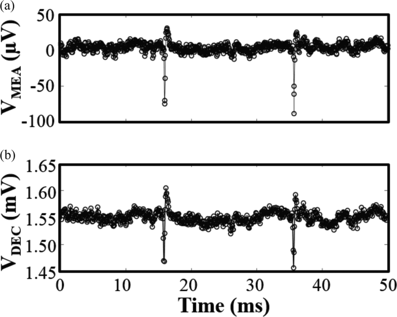
To confirm MOTE’s neural recording capability, we have played a pre-recorded neural signal, acquired through a commercial MEA, into a MOTE whose inputs are wire-bonded out to connectors on a PCB. Fig. 13 compares the original neural signal (~100 μVPP spikes sampled at 20 KHz) acquired by the MEA (Fig. 13(a)) to the decoded optical pulses from MOTE (Fig. 13(b)) to prove that the MOTE is indeed capable of detecting and transmitting neural signals. The root-mean-squared-error between ground-truth input and reconstructed MOTE output is <15 μVRMS, consistent with input referred noise levels. This measurement is addition to the neural recording of composite spikes in a live, anesthetized invertebrate in our previous work [20].
Fig. 13.
Pre-recorded neural signal measured through a MOTE: (a) an original neural signal (~100 μVPP spikes) recorded through a MEA at fSAMPLE = 20 KHz; (b) the pre-recorded neural signal is fed into a MOTE, which of output optical pulses can be decoded to faithfully retrieve the MEA’s neural recording.
IV. Heterogeneous Integration on CMOS
A. AlGaAs PVLED
The PVLED developed for this work is an AlGaAs/GaAs heterostructure designed to function both as a PV for visible light and a LED emitting at longer, near-infrared wavelengths. By having slightly thicker AlGaAs barrier layers between the quantum wells in the active region of the AlGaAs/GaAs heterostructure than in a typical LED, we are able to produce a device that is sufficiently efficient in performing both functions. The PVLED is grown on top of a heavy aluminum-content Alo.9Gao.1As layer to enable a thin (~1 μm) PVLEDs to be released from the substrate and transferred using techniques similar to those that have been more widely used for transferable micro-LEDs [45,46] as well as 2 dimensional (2D) materials [47].
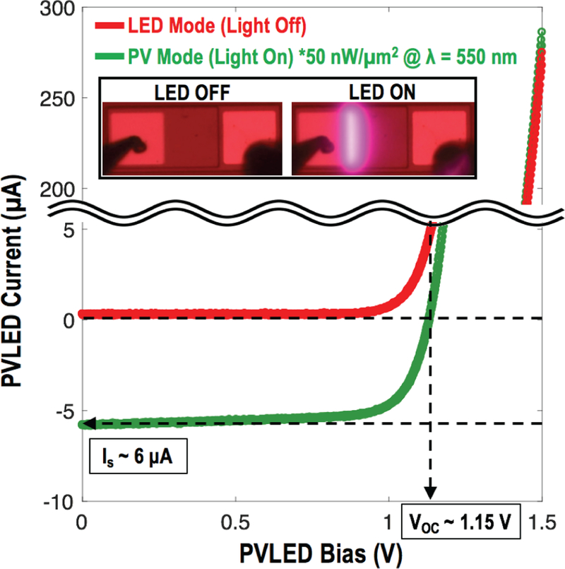
Fig. 14 presents the PVLED in its PV and LED modes of operation which have implications in available power and required LED-driving current. About 98 % of the time, the PVLED acts as a power source, transducing incoming light into electrical power, providing at least 1 μA at ~1 V. During the remaining ~2 % of the time, the PVLED acts as an optical transmitter, emitting optical pulses to transmit encoded measurement data to an external receiver at a longer wavelength. Again, this allows the system to be more compact than the previously reported RF [9] and ultrasonic [14, 15] approaches.
Fig. 14.
LED and PV modes of operation for AlGaAs PVLED employed in the presented work [20].
B. Fabrication for Integrating CMOS with PVLED
Prior to transferring PVLED onto CMOS, the CMOS die is etched with CF4 plasma (Oxford PlasmaLab 80 RIE System) to remove the passivation (SiO2) over the top metal of the CMOS, with the top metal, aluminum, acting as an inherent etch stop [48], Following the transfer, the PVLED is clamped down using highly conformai atomic layer deposition (ALD, Oxford ALD FlexAL) of 50 nm thick SiO2 film. Then, the SiO2 is selectively removed using contact lithography (ABM Contact Aligner) followed by buffered oxide etch (BOE) to open up contacts to the CMOS and the PVLED. CMOS-PVLED routing is subsequently established through Pt sputtering (ATC-Orion 5 UHV with Load-Lock by AJA International INC). We have chosen sputtering for metal deposition to ensure that the Pt is continuous over the highly nonplanar surface between CMOS and PVLED contacts.
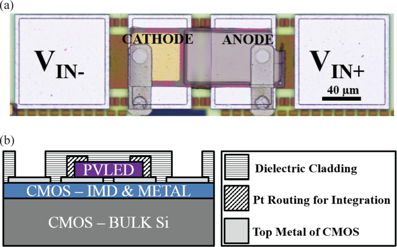
Fig. 15 illustrates a fully integrated MOTE where Fig. 15(a) shows a die photograph of the MOTE. Fig. 15(b) shows a crosssectional diagram to better illustrate the integration. The system can then be encapsulated using parylene C to make it biocompatible [49], In order to verily the bio-compatibility, we have immersed the MOTE in a phosphate-buffered solution (PBS, Gibco 10010023, pH 7.4 (IX)), and have verified survival up to 77 hours. It should be noted that the CMOS chip employed for this integration testing has the top metal foot-print (circuits and PVLED width is still ~57 μm) larger than 57 μm in width for ease of testing the fabrication flow.
Fig. 15.
A fully integrated MOTE: (a) a die photograph of an integrated MOTE [20]; (b) simplified cross-sectional view of the MOTE.
V. Discussion
The presented work provides an overview on the feasibility of a microscale tetherless, optoelectronic neural recording unit, as well as initial proof-of-concept prototype electronics for such a system. While the MOTE demonstrates that the circuits and heterogeneous integration of such unit is possible, there is much room for further improvement in size and performance, and further verification through deployed MOTEs.
A. Design Robustness and Scaling
Although the present generation MOTE design worked in all five chips tested, some performance parameters were not as reliable as expected. In particular, the high pass comer was both variable and lower in frequency than expected, likely due to imperfect modelling/process variation at very low powers. Similarly, our startup circuits were not as reliable as desired under slow optical wake-up, and we plan to investigate a different wakeup/reset schemes.
At the same time, the cross-section of the implemented MOTE can certainly be reduced. Our ultimate goal is scaling down the diameter/cross-sectional width to 10–20 μm [37] while keeping the length at 100~200 μm range to provide sufficient electrodes separation for robust voltage sensing.
While the thickness of the MOTE can be reduced to 10~20 μm by etching away most of the bulk Si using deep reactive ion etch, reducing the width requires shrinking circuit building blocks without degrading performance. A faster oscillator, combined with small digital frequency dividers for sampling, could allow for the use of switched capacitor techniques to achieve low-pass filters with much less physical capacitance [4], Further size reduction requires moving to a more advanced CMOS process, such as 65nm. Scaling will provide significant help in shrinking all digital functions, bias circuits and interconnects (wires). In addition, for the same number of metal layers, a 65 nm process interconnect stack is significantly shorter than in 180 nm, reducing ‘height’ as well as width. Unfortunately, process scaling may not help with capacitance density, since thin-oxide MOSCAPs can have excessive current leakage, and 65 nm CMOS only provides a modest enhancement in flicker noise as a function of gate area. Still, we estimate that translating our designs to 65 nm CMOS, combined with a faster clock and a mild degradation in flicker noise could take us to a 20 μm cross-section. Moreover, as our system requirements are further understood, additional opportunities for optimization will present themselves.
B. Effect of Scattering
For IR wavelength in brain, the reduced scattering coefficient is about 1 mm−1 [50], which describes the depth where photons lose their initial directional memory and become diffusive. MOTEs implemented few mm’s deep into a brain will mainly see the scattered photons, and the scattered photons (i.e., diffusive photons) at the depth will provide approximately orientation-insensitive powering.
C. Insertion and Encapsulation Techniques
Although most of the technology for a useful MOTE has been demonstrated here, it has not yet been demonstrated that such MOTES can be deployed and function in-vivo, especially over chronic timescales.
One area of development not discussed here is techniques for implanting MOTEs in tissue. A number of techniques are possible, and preliminary work indicates that attaching MOTES to custom shanks with a soluble, biocompatible material such as PEG can allow insertion and release of MOTE-scale implants in the mouse brain.
A related problem is appropriate encapsulation of MOTEs to allow reliable chronic implantation. Preliminary studies indicate that encapsulation using a combination of atomic layer deposition (ALD) of Si02, SixNy, and parylene, often used for biological coatings [49, 51], should allow for >1 year of deployment. In addition, the silicon substrate of the CMOS requires an opaque coating (such as metal) to prevent excessive optical generation of carriers that can generate unwanted currents in the CMOS circuits.
VI. Conclusion
In this work, we have presented the technology for tetherless neural recording that combines the merits of both optical and electrical modalities. While the optics provides means for deep penetration for power transfer as well as signal communication, electronics provides means for efficient use of the delivered optical power for low noise measurements. We have started by identifying biological safety as well as fundamental device limits of the proposed techniques, applied engineering safety factors, and made designs accordingly. As shown in the preliminary characterization above, we have successfully demonstrated that an AlGaAs PVLED can be integrated with commercial CMOS at the back end of the line with minimal post-fabrication and without imposing any unconventional changes on CMOS fabrication flow. Furthermore, the integrated system was indeed capable of providing low noise measurement of neural signals.
Table I compares the MOTE against other tetherless neural recording schemes. While our BW is comparable to other tetherless techniques and noise floor compares favorably, the MOTE truly stands out in terms of its dimensions per channel. Although there is still much work to be done in order to demonstrate that MOTE can indeed be employed for recording neurophysiological signals of mammalian brain in vivo, in particular in developing minimally-invasive insertion techniques, this work paves a path towards one of the more promising directions in realizing a micro-scale tetherless neural recording unit.
TABLE I.
Table of Comparison against Arts
| Integrated Neural Interface [9] | Microwave Back-scattering [54] | WINeR probes [11] | Neural Dust [14] | MOTE | |
|---|---|---|---|---|---|
| Power Source | RF Coil | RF | RFCoil | Ultrasonic | Optical |
| Gain(dB) | 60 | - | 40 | - | 30 |
| BW(KHz) | 5 | 5 | 8 | > 30 | > 10 |
| Noise Floor | 5.1 μ VRMS | 63 μ VRMS | 5.4 μ VRMS | 180 μ VRMS | ~ 15 μVRMS |
| DC Power | 135 μ W† | NA | 19.3 μW† | NA | < 1 μW |
| Volume(mm3) | > 10 | 360 | > 4‡ | 2.4 | 4.7 × 10⁻³* |
| Weight‡(μg) | > 2.3 × 10⁴ | > 8.38 × 10⁵ | > 9300 | > 7600 | 11 |
| Min. Cross-section | > 0.3 mm | > 10 mm | > 0.3 mm | > 0.5 mm | 50 μm |
Per channel
Estimated
Die thickness of 330 μm multiplied by circuit dimensions, can further be reduced by die thinning.
Acknowledgment
The authors would like to thank Chris Xu, Jesse H. Goldberg, Haining Wang, and Changhyuk Lee for critical discussions.
Research reported herein was supported by the National Institutes ofHealth under award number 1R21EY027581. This work was performed in part at the Cornell NanoScale Facility, a member of the National Nanotechnology Coordinated Infrastructure (NNCI), which is supported by the National Science Foundation (Grant ECCS-1542081), and made use of the Cornell Center for Materials Research Facilities supported by the National Science Foundation under Award Number DMR-1120296.
Biographies

Sunwoo Lee (M’2010) received the B.S. degree in electrical and computer engineering from Cornell University, Ithaca, NY, USA, in 2010, and the M.S. and Ph.D. degrees in electrical engineering from the Columbia University, NY, USA, in 2012 and 2016, respectively, working graphene-based nano-electro-mechanical systems for signal processing and sensing applications.
In April 2016 he joined the Molnar Group as a postdoctoral researcher in the School of Electrical and Computer Engineering, Cornell University, Ithaca, NY, USA, to work on opto-electrically transduced micro-scale neural interfaces.

Alejandro Javier Cortese received the B. S. degree in Physics with highest honors and the B.S. degree in Mathematics from Duke University, Durham, NC, USA in 2012, and the M.S degree in Physics from Cornell University, Ithaca, NY, USA in 2015. Currently, he is a PhD candidate with the McEuen Group in the Physics Department at Cornell University, Ithaca, NY USA working on wireless optoelectronic sensors.

Aasta Parin Gandhi is a junior in electrical and computer engineering department at Cornell University, Ithaca, NY, USA. Her research interests include the brain-computer interface.

Elizabeth Rose Agger received the B.A. degree in neuroscience and film studies at Wesleyan University, Middletown, CT, USA, in 2010, the B.S. degree in electrical and computer engineering at the University of Maryland, College Park, MD, USA, in 2013, and the M.S. degree in electrical and computer engineering from Cornell University, Ithaca, NY, USA, in 2017.

Paul L. McEuen received the B.S. degree in engineering physics at the University of Oklahoma, Norman, OK, USA in 1985, and Ph.D. in applied physics at Yale University, New Haven, CT, inl991.
From 1990 to 1991, he worked as a postdoctoral researcher at MIT, Cambridge, MA, USA, before joining the faculty of the University of California, Berkeley, CA, USA. He moved to Cornell University in 2001, where he is currently the John A. Newman Professor of Physical Science. He is a member of the National Academy of Sciences and American Physical Society Fellow.

Alyosha Christopher Molnar (M’2007-S’2018), received the B.S. degree in engineering with highest honors from Swarthmore College, Swarthmore, PA, USA, in 1997, and the M.S. and Ph.D. degrees in electrical engineering from the University of California, Berkeley, CA, USA, in 2003 and 2007, respectively.
From 1998 to 2002, he was with the RF IC Group at Conexant Systems, Inc. (now Skyworks Solutions, Inc.), Newport Beach, CA, USA, where he developed their first-generation GSM direct conversion receiver. In August 2007 he joined the faculty of the School of Electrical and Computer Engineering, Cornell University, Ithaca, NY, USA.
Contributor Information
Sunwoo Lee, Department of Electrical and Computer Engineering, Cornell University in Ithaca, 14853 USA.
Alejandro J. Cortese, Department of Physics, Cornell University in Ithaca, 14853 USA
Aasta Gandhi, Department of Electrical and Computer Engineering, Cornell University in Ithaca, 14853 USA.
Elizabeth R. Agger, Department of Electrical and Computer Engineering, Cornell University in Ithaca, 14853 USA
Paul L. McEuen, Department of Physics, Cornell University in Ithaca, 14853 USA
Alyosha C. Molnar, Department of Electrical and Computer Engineering, Cornell University in Ithaca, 14853 USA.
References
- [1].Alivisatos A, Chun M, Church G, Greenspan R, Roukes M and Yuste R, “The brain activity map project and the challenge of functional connectomics,” Neuron, vol. 74, no. 6, pp. 970–974, 2012. [DOI] [PMC free article] [PubMed] [Google Scholar]
- [2].Schenck JF, “The role of magnetic susceptibility in magnetic resonance imaging: MRI magnetic compatibility of the first and second kinds,” Medical Physics, vol. 23, no. 6, pp. 815–850, June 1996. [DOI] [PubMed] [Google Scholar]
- [3].“https://www.braininitiative.nih.gov/,” [Online].
- [4].Johnson B, Peace ST, Wang A, Cleland TA and Molnar A, “A 768-Channel CMOS Microelectrode Array With Angle Sensitive Pixels for Neuronal Recording,” in lEEESensorsJournal, vol. 13, no. 9, pp. 3211–3218, September 2013. [Google Scholar]
- [5].Dragas J, Viswam V, Shadmani A, Chen Y, Bounik R, Stettler A, Radivojevic M, Geissler S, Obien MEJ, Müller J and Hierlemann A, “In Vitro Multi-Functional Microelectrode Array Featuring 59 760 Electrodes, 2048 Electrophysiology Channels, Stimulation, Impedance Measurement, and Neurotransmitter Detection Channels,” in IEEE Journal of Solid-State Circuits, vol. 52, no. 6, pp. 1576–1590, June 2017. [DOI] [PMC free article] [PubMed] [Google Scholar]
- [6].Bai Q, Wise K and Anderson D, “A high-yield microassembly structure for three-dimensional microelectrode arrays,” in IEEE ‘Transactions on Biomedical Engineering, vol. 47, no. 3, pp. 281–289, March 2000. [DOI] [PubMed] [Google Scholar]
- [7].Buzsaki G, Stark E, Berényi A, Khodagholy D, Kipke D, Yoon E and Wise KD, “Tools for Probing Local Circuits: High-Density SiliconProbes Combined with Optogenetics,” Neuron, vol. 86, no. 1, pp. 92–105, April 2015. [DOI] [PMC free article] [PubMed] [Google Scholar]
- [8].Michon F, Aarts A, Holzhammer T, Ruther P, Borghs G, McNaughton B and Kloosterman F, “Integration of silicon-based neural probes and micro-drive arrays for chronic recording of large populations of neurons inbehaving animals,” Journal of Neural Engineering, vol. 13, no. 4, p. 046018, June 2016. [DOI] [PubMed] [Google Scholar]
- [9].Harrison R, Watkins P, Kier R, Lovejoy R, Black D, Normann R and Solzbacher F, “A Low-Power Integrated Circuit for a Wireless 100-Electrode Neural Recording System,” in 2006 IEEE International Solid State Circuits Conference - Digest of Technical Papers, San Francisco, CA, pp. 2258–2267, 2006. [Google Scholar]
- [10].Jiang Z, Huxter JR, Bowyer SA, Blockeei AJ, Butler J, Imtiaz SA, Wafford KA, Phillips KG, Tricklebank MD, Marston HM and Rodriguez-Villegas E, “TaiNi: Maximizing research output whilst improving animals’ welfare in neurophysiology experiments,” Scientific Reports, vol. 7, no. 1, p. 8086, 2017. [DOI] [PMC free article] [PubMed] [Google Scholar]
- [11].Lee SB, Lee B, Kiani M, Mahmoudi B, Gross R and Ghovanloo M, “Fabrication and Microassembly of a mm-Sized Floating Probe for a Distributed Wireless Neural Interface,” in IEEE Sensors Journal, vol. 16, no. 2, pp. 475-484, 15 January 2016.27069422 [Google Scholar]
- [12].Szarowski D, Andersen M, Retterer S, Spence A, Isaacson M, Craighead H, Turner J and Shain W, “Brain responses to micro-machined silicon devices,” Brain Research, vol. 983, no. 1–2, pp. 23–35, 2003. [DOI] [PubMed] [Google Scholar]
- [13].Khalifa A, Karimi Y, Wang Q, Garikapati S, Montlouis W, Stanacevic M, Thakor N and Etienne-Cummings R, “The Microbead: A Highly Miniaturized Wirelessly Powered Implantable Neural Stimulating System,” in IEEE Transactions on Biomedical Circuits andSystems, vol. 12, no. 3, pp. 521–531, June 2018. [DOI] [PubMed] [Google Scholar]
- [14].Seo D, Neely RM, Shen K, Singhal U, Alon E, Rabaey JM, Carmena JM and Maharbiz MM, “Wireless Recording in the Peripheral Nervous System with Ultrasonic Neural Dust,” Neuron, vol. 91, no. 3, pp. 529–539, August 2016. [DOI] [PubMed] [Google Scholar]
- [15].Wirdatmadja SA, Balasubramaniam S, Koucheryavy Y and Jomet JM, “Wireless optogenetic neural dust for deep brain stimulation,” in IEEE 18th International Conference on e-Health Networking, Applications and Services (Healthcom), Munich, pp. 1–6, 2016. [Google Scholar]
- [16].Seo D, Carmena JM, Rabaey JM, Alon E and Maharbiz MM, “Neural Dust: An Ultrasonic, Low Power Solution for Chronic Brain-Machine Interfaces,” arXiv:1307.2196, 2013. [Google Scholar]
- [17].Yuste R and Katz LC, “Control of postsynaptic calcium influx in developing neocortex by excitatory and inhibitory neurotransmitters,” Neuron, vol. 6, no. 3, pp. 333–344, 1991. [DOI] [PubMed] [Google Scholar]
- [18].Prevedel R, Yoon Y-G, Hoffmann M, Pak N, Wetzstein G, Kato S, Schrödel T, Raskar R, Zimmer M, Boyden DS and Vaziri A, “Simultaneous whole-animal 3D imaging of neuronal activity using light-field microscopy,” NatureMethods, vol. 11, no. 7, pp. 727–730, 2014. [DOI] [PMC free article] [PubMed] [Google Scholar]
- [19].Yang W and Yuste R, “Invivo imaging of neural activity,” NatureMethods, vol. 14, no. 4, pp. 349–359, April 2017. [DOI] [PMC free article] [PubMed] [Google Scholar]
- [20].Lee S, Cortese AJ, Trexel P, Agger ER, McEuen PL and Molnar AC, “A 330μm×90μm opto-electronically integrated wireless system-on-chip for recording of neural activities,” in 2018 IEEE International Solid State Circuits Conference - Digest of Technical Papers, San Francisco, CA, pp. 292–294, 2018. [Google Scholar]
- [21].Dimagl U, Einhäupl K and Villringer A, Optical Imaging ofBrain Function and Metabolism - Volume 333 of Advances in Experimental Medicine and Biology, Springer Science & Business Media, LLC, July 1992, pp. 48–54. [Google Scholar]
- [22].Haydaroglu I and Mutlu S, “Optical PowerDelivery and Data Transmission in a Wireless and Batteryless Microsystem Using a Single Light Emitting Diode,” Journal of Microelectromechanical Systems, vol. 24, no. 1, pp. 155–165, February 2015. [Google Scholar]
- [23].Haydaroglu I, Ozgun MT and Mutlu S, “Optically Powered Optical Transmitter Using a Single Light-Emitting Diode,” in IEEE Transactions on Circuits and Systems I: RegularPapers, vol. 64, no. 8, pp. 2003–2012, 2017. [Google Scholar]
- [24].Podgorski K and Ranganathan G, “Brain heating induced by near-infrared lasers during multiphoton microscopy,” Journal of Neurophysiology, vol. 116, no. 3, pp. 1012–1023, 2016. [DOI] [PMC free article] [PubMed] [Google Scholar]
- [25].Bevilacqua F, Piguet D, Marquet P, Gross JD, Tromberg BJ and Depeursinge C, “Invivo local determination of tissue optical properties: applications to humanbrain ”AppliedOptics, vol. 38, no. 22, pp. 4939–4950, 1999. [DOI] [PubMed] [Google Scholar]
- [26].Y. J a. Backman V, “Imaging a full set of optical scattering properties ofbiological tissue by inverse spectroscopic optical coherence tomography,” Optics Letters, vol. 37, no. 21, pp. 4443–4445, 2012. [DOI] [PMC free article] [PubMed] [Google Scholar]
- [27].Laboratory NRE, “Research Cell Efficiency Records,” U.S. Departmentof Energy, September 2015. [Online]. Available: https://www.energy.gov/eere/solar/downloads/research-cell-efficiency-records. [Accessed 30 August 2018].
- [28].Yaroslavsky AN, Schulze PC, Yaroslavsky IV, Schober R, Ulrich F and Schwarzmaier H-J, “Optical properties of selected native and coagulated human brain tissues in vitro in the visible and near infrared spectral range,” Physics in Medicine & Biology, vol. 47, no. 12, pp. 2059–2073, June 2002. [DOI] [PubMed] [Google Scholar]
- [29].Hemmati H, Biswas A and Djordjevic IB, “Deep-Space Optical Communications: Future Perspectives and Applications,” Proceedings of the IEEE, vol. 99, no. 11, pp. 2020–2039, August 2011. [Google Scholar]
- [30].Van Der Ziel A, Noise: sources, characterization, measurement, New York (70 Fifth Avenue): Prentice-Hall, 1954. [Google Scholar]
- [31].Steyaert MSJ and Sansen WMC, “A micropower low-noise monolithic instrumentation amplifier for medical purposes,” in IEEE Journal of Solid-State Circuits, vol. 22, no. 6, pp. 1163–1168, December 1987. [Google Scholar]
- [32].Harrison R and Charles C, “A low-power low-noise CMOS amplifier for neural recording applications,” in IEEE Journal of Solid-State Circuits, vol. 38, no. 6, pp. 958–965, June 2003. [Google Scholar]
- [33].Johnson B and Molnar A, “An Orthogonal Current-Reuse Amplifier for Multi-Channel Sensing,” in IEEE Journal of Solid-State Circuits, vol. 48, no. 6, pp. 1487–1496, June 2013. [Google Scholar]
- [34].Shen L, Lu N and Sun N, “A IV 0.25uW inverter-stacking amplifierwith 1.07 noise efficiency factor,” 2017 Symposium on VLSI Circuits, Kyoto, pp. C140–C141,2017. [Google Scholar]
- [35].Tsividis Y and McAndrew C, Operation and Modeling of the MOS Transistor, 3rd ed, New York: OXFORD UNIVERSITY PRESS, 2011. [Google Scholar]
- [36].Ouzounov DG, Wang T, Wang M, Feng DD, Horton NG, Cruz-Hemandez JC, Cheng Y-T, Reimer J, Tolias AS, Nishimura N and Xu C, “Invivo three-photon imaging of activity of GCaMP6-labeled neurons deep in intact mouse brain,” Nature Methods, vol. 14, pp. 388–390, February 2017. [DOI] [PMC free article] [PubMed] [Google Scholar]
- [37].Guitchounts G, Markowitz JE, Liberti WA and Gardner TJ, “A carbon-fiber electrode array for long-term neural recording,” Journal of Neural Engineering, vol. 10, no. 4, p. 046016, July 2013. [DOI] [PMC free article] [PubMed] [Google Scholar]
- [38].Hosticka BJ, “Dynamic CMOS amplifiers,” in lEEE Journal of Solid-State Circuits, vol. 15, no. 5, pp. 881–886, 1980. [Google Scholar]
- [39].Krummenacher F, “Micropowerswitched capacitor biquadratic cell,” in IEEE Journal of Solid-State Circuits, vol. 17, no. 3, pp. 507–512, 1982. [Google Scholar]
- [40].Knitel MJ, Woerlee PH, Schölten AJ and Duijnhoven AZ-V, “Impact of process scaling on 1/f noise in advanced CMOS technologies,” in International Electron Devices Meeting 2000 Technical Digest. IEDM (Cat. No.00CH37138), SanFrancisco, CA, USA, pp. 463–466, 2000. [Google Scholar]
- [41].Horton NG, Wang K, Kobat D, Clark CG, Wise FW, Schaffer CB and Xu C, “Invivo three-photon microscopy of subcortical structures within an intact mouse brain,” Nature Photonics, vol. 7, pp. 205–209, January 2013. [DOI] [PMC free article] [PubMed] [Google Scholar]
- [42].Donati S, Photodetectors: Devices, Circuits, And Applications, Upper Saddle River, NJ: Prentice Hall PTR, 2000. [Google Scholar]
- [43].Thorlabs, “https://www.thorlabs.com,” 6 July 2018. [Online] Available: https://www.thorlabs.com/drawings/6al721d77e0a5adf-05AB30CB-0CF0-F7EE-28EF9528DA9214B6ZAPD410A-Manual.pdf. [Accessed 14 July 2018].
- [44].Guillory KS and Normann RA, “A 100-channel system for real time detection and storage of extracellular spike waveforms,” Journal of Neuroscience Methods, vol. 91, no. 1–2, pp. 21-29, 15 September 1999. [DOI] [PubMed] [Google Scholar]
- [45].Yoon J, Jo S, Chun IS, Jung I, Kim H-S, Meitl M, Menard E, Li X, Coleman JJ, Paik U and Rogers JA, “GaAs photovoltaics and optoelectronics using releasable multilayer epitaxial assemblies,” Nature, vol. 465, pp. 329–333, May 2010. [DOI] [PubMed] [Google Scholar]
- [46].Park S-I, Xiong Y, Kim R-H, Elvikis P, Meitl M, Kim D-H, Wu J, Yoon J, Yu C-J, Liu Z, Huang Y, Hwang K.-c., Ferreira P, Li X, Choquette K and Rogers JA, “Printed Assemblies of Inorganic Light-Emitting Diodes for Deformable and Semitransparent Displays,” Science, vol. 325, no. 5943, pp. 977–981, August 2009. [DOI] [PubMed] [Google Scholar]
- [47].Li X, Cai W, An J, Kim S, Nah J, Yang D, Piner R, Velamakanni A, Jung I, Tutuc E, Banerjee SK, Colombo L and Ruoff RS, “Large-Area Synthesis of High-Quality and Uniform Graphene Films on Copper Foils,” Science, vol. 324, no. 5932, pp. 1312–1314, 2009. [DOI] [PubMed] [Google Scholar]
- [48].Lee S, Applications of Graphene-based Nano Electro Mechanical Systems, New York, NY, USA: Columbia University Academic Commons, 2016. [Google Scholar]
- [49].Xianzong Xie LR, Caldwell R, Diwekar M, Tathireddy P, Sharma R and Solzbacher F, “Long-Term Bilayer Encapsulation Performance of Atomic Layer Deposited A1203 and Parylene C for Biomedical Implantable Devices,” in IEEE ‘Transactions on Biomedical Engineering, vol. 60, no. 10, pp. 2943–2951, October 2013. [DOI] [PubMed] [Google Scholar]
- [50].Bevilacqua F, Piguet D, Marquet P, Gross JD, Tromberg BJ and Depeursinge C, “Invivo local determination of tissue optical properties: applications to humanbrain “Applied Optics, vol. 38, no. 22, pp. 4939–4950, 1999. [DOI] [PubMed] [Google Scholar]
- [51].Burgess TE, Bauma JC, Fowkesb FM, Holmstromc R and Shim GA, “Thermal Diffusion of Sodium in Silicon Nitride Shielded Silicon Oxide Films,” Journal of The Electrochemical Society, vol. 116, no. 7, pp. 1005–1008, 1969. [Google Scholar]
- [52].Guitchounts G, Markowitz JE, Liberti WA and Gardner TJ, “A carbon-fiber electrode array for long-term neural recording,” Journal of Neural Engineering, vol. 10, no. 4, p. 046016, 2013. [DOI] [PMC free article] [PubMed] [Google Scholar]
- [53].Johnson B, Peace ST, Wang A, Cleland TA and Molnar A, “A 768-Channel CMOS Microelectrode Array With Angle Sensitive Pixels for Neuronal Recording,” in IEEE Sensors Journal, vol. 13, no. 9, pp. 3211–3218, September 2013. [Google Scholar]
- [54].Kiourti A, Lee C, Chae J and Volakis J, “A Wireless Fully Passive Neural Recording Device for Unobtrusive Neuropotential Monitoring,” in IEEE ‘Transactions on Biomedical Engineering, vol. 63, no. 1, pp. 131–137, January 2016. [DOI] [PubMed] [Google Scholar]


