

Abstract
The combination of materials with targeted optical properties and of complex, 3D architectures, which can be nowadays obtained by additive manufacturing, opens unprecedented opportunities for developing new integrated systems in photonics and optoelectronics. The recent progress in additive technologies for processing optical materials is here presented, with emphasis on accessible geometries, achievable spatial resolution, and requirements for printable optical materials. Relevant examples of photonic and optoelectronic devices fabricated by 3D printing are shown, which include light‐emitting diodes, lasers, waveguides, optical sensors, photonic crystals and metamaterials, and micro‐optical components. The potential of additive manufacturing applied to photonics and optoelectronics is enormous, and the field is still in its infancy. Future directions for research include the development of fully printable optical and architected materials, of effective and versatile platforms for multimaterial processing, and of high‐throughput 3D printing technologies that can concomitantly reach high resolution and large working volumes.
Keywords: 3D printing, additive manufacturing, direct ink writing, electrospinning, light‐emitting devices, optical sensors, waveguides
1. Introduction
Additive manufacturing (AM) is experiencing a rapid evolution in its relevant technologies, which are constantly shifting from object prototyping at small scale to much more comprehensive fabrication platforms. Currently available AM techniques encompass various methods, categorized in seven groups highlighting the basic mechanism used for material processing.1, 2 Most of additive technologies exploit either curing of a photosensitive material by exposure to light, or the direct deposition of inks or solutions with suitable viscoelastic properties, to build 3D objects in a layer‐by‐layer fashion, starting from a digital model. Materials printable by AM methods include polymers,3 metals,4, 5 ceramics,6 nanocomposites,7 and soft matter.8 In this way, components with unprecedented complex geometries can be obtained, with potential impact in numerous fields, such as aerospace and automotive,9, 10 tissue engineering,11, 12 microfluidics,13, 14 and energy storage.15
The interest toward AM methods is mainly motivated by their capability of generating 3D items with elaborate architecture, and by the possibility of remarkably simplifying the design of devices, making it more stable and robust. AM technologies also allow material waste to be greatly reduced compared to conventional top‐down manufacturing. Furthermore, at variance with conventional optical or electron‐beam lithographies, AM methods allow devices to be printed or manufactured on nonplanar surfaces, curvilinear substrates, and tortuous 3D patterns.16 For instance, through preliminary scanning of real surfaces, their shape can be precisely considered in the digital design of the desired object, as well as in the manufacturing process. In turn, such flexibility leads to new opportunities for system integration, allowing different components of a multipart functional system to be assembled and interconnected along the out‐of‐plane direction, that is, along the third (vertical) spatial dimension. All these aspects are of paramount importance in the fields of photonics and optoelectronics, where most of components (light sources, lasers, lenses, waveguides, and photodetectors) have been traditionally pushed in either planar geometries or, when presenting simple 3D shapes (e.g., cylindrical or spherical, or combination of them) have been mostly assembled in planar configurations. In the last decade, instead, many truly 3D photonic components have emerged, featuring a range of novel or improved optical properties or device characteristics. These systems include 3D photonic crystals and metamaterials,17, 18 where the light propagation and light–matter interaction can be precisely tailored to enhance reflection, absorption, and amplification in specific spectral bands, 3D interferometers,19, 20 and omnidirectional optical couplers for improved injection and extraction of photons.21 Furthermore, the manipulation of light by 3D free‐form optical components and lenses with aspheric surfaces is expected to enhance optical resolution and to compensate aberrations in vision components for robots, drones, and, more generally, autonomous movable systems.22 Finally, 3D printing might critically support the integration of optoelectronics in soft, nonplanar systems. These can include gloves, bioimplants, endoscopes, catheters, contact lenses, glasses, and optical fibers, leading to new approaches for real‐time monitoring of physiological parameters in medical applications,23, 24, 25 production of injectable devices for optogenetics,26 and enhancement of the sensorial experience in augmented and virtual reality.27, 28, 29
However, the development of 3D photonics and optoelectronics has been slowed down by a few stringent requirements associated to these applications, in terms of i) optical properties of the used materials, ii) spatial resolution needed to be achieved by the fabrication processes, and iii) necessary uniformity of the interfaces between diverse materials. All these issues greatly affect the performance of optical devices. For instance, the transport of light along a passive waveguide is affected by propagation losses made up by the sum of several contributions:30 the absorption of the used material at the frequency of the propagating light, the Rayleigh scattering by inhomogeneities of the bulk (i.e., local variations of the refractive index, density, composition), the Rayleigh scattering by defects at the waveguide surface, and leakages due to light coupling with the surrounding materials or environment. In order to realize these components additively, first printable materials have to be developed with low absorption at the target wavelengths. In addition, these materials should exhibit well‐suited optical properties (e.g., luminescence, optical gain, nonlinear optical response) in order to build active and functional photonic elements. Preserving the function of active materials during printing might be challenging, since the use of UV radiation or processing at high temperature might modify the absorption and emission bands, decrease the emission quantum yield, and suppress optical gain in many organic compounds.31, 32 Finally, a tight process control is needed to print with high uniformity both in the bulk and at interfaces, thus reducing undesired losses due to light scattering. The quality of interfaces is also critical for those devices, such as light‐emitting diodes (LEDs) or solar cells, where charge injection or extraction is present and where optically active layers are adjacent to metals or to hole‐ and electron‐transporting layers, because the presence of defects and trap states greatly decreases the efficiency of the current‐to‐light or light‐to‐current conversion.
This progress report presents the recent progress in AM technologies specifically addressed to the fabrication of photonic and optoelectronic devices, and a few perspective directions for this vibrant field. The most promising approaches are reviewed, with focus on available printable optical materials, resolution achievable, generated geometries, and on the additive fabrication of light sources, waveguides, photonic crystals and metamaterials, optical sensors, and microscale optical components. In the last section, future challenges and opportunities of 3D printing technologies for photonics and optoelectronics are presented and discussed.
2. Light Exposure‐Based Additive Technologies
Light interacting with photosensitive materials can trigger a series of chemical reactions, which can be exploited to produce patterns with micrometric or sub‐micrometric resolution.3 This is what is commonly done in photolithography, where UV light is used to pattern a resist by texturing a beam through a photomask, which contains the motifs to be transferred. Similarly, in direct laser writing,33, 34 a laser beam is directed on the resist, modifying locally the chemicophysical properties of the organic layer, and the desired pattern is realized by scanning the beam. UV photolithography and laser writing allow 2D microstructures to be generated, and they are widely used for industrial production in microelectronics, optoelectronics, and photonics. The extension of photopolymerization methods to the fabrication of complex, 3D items is accomplished by implementing a layer‐by‐layer approach, in which the desired object is sliced in various 2D layers which are built consecutively, each individual layer being obtained by exposing a photosensitive material to structured light or to a scanning laser beam, similarly to photolithography and to laser writing.
2.1. Stereolithography
The invention of stereolithography (STL) by C. Hull in 198635 has opened the field of 3D printing, enabling the fabrication of 3D components through the photopolymerization of UV‐sensitive resins. In a typical STL process, an UV laser beam is focused on a liquid prepolymer, composed of suitable monomers and/or oligomers, and photoinitiators triggering the polymerization reaction. Curing can occur through the production of free radicals, the generation of cationic species, and other pathways.36, 37, 38 Critical process parameters are typically given by the concentration of photoinitiators, the intensity of the laser and its in‐plane scanning speed.39 For instance, a characteristic light dose is required to initiate the formation of the polymer network, which is related, among other variables, to the absorption coefficient of the photoinitiators and to the concentration of dissolved oxygen (which generally inhibits the polymerization process). Similar considerations hold for the photopoly‐merization rate.39 Recently, geometrical constraints, confining the volume of photocurable polymers, have also been found to modify the curing kinetics,40 slowing down polymerization and introducing a complex temporal behavior (polychromatic process). This aspect might be pivotal for building objects made by nanocomposite materials, where the addition of nanoparticles in the prepolymeric resin can introduce geometrical constraints and heterogeneous interfaces, significantly affecting the development of polymer networks during photopolymerization. For example, the addition of silica nanoparticles to a mixture of acrylate‐functionalized oligomers leads to an increase of the light dose needed to fully polymerize the nanocomposite,41 and quantum dots (QDs) are found to decrease the polymerization rate of acrylate monomers.42
In addition, the inclusion of nanoparticles to prepolymers raises some concerns for the potential increase of opacity and the spatial variations of the refractive index, leading to light scattering. Preventing particle aggregation and improving the stability of suspensions in photocurable resins through organic surface modifiers greatly help in producing transparent 3D printed nanocomposites (optical transmission > 90% in the 400–1100 nm spectral range).41 Used with laser STL, this approach also reduces the shrinkage and distortions in printed structures, improving the resulting mechanical properties.41
The choice of the monomers and oligomers in resins for STL depends on the final desired application. Acrylate‐based compounds are widely used in photonics due to their good optical transparency.3 However, the variety of relevant materials printable by UV STL is continuously increasing, an effort which is also motivated by some disadvantages related to the use of acrylates such as yellowing upon aging, limited mechanical properties, and poor biocompatibility.3 In such framework, glass is the material of choice for many optical components (lenses, optical fibers, optical windows). Recently, a STL approach for processing fused silica glass has been introduced,43 which is based on using a nanocomposite prepolymer with amorphous silica nanoparticles dispersed in a photocurable matrix of the monomer hydroxyethylmethacrylate (Figure 1 a). The nanocomposite prepolymer solidifies in 3D upon STL, and a two‐step, postprinting thermal treatment is carried out to convert the printed object to fused silica glass. At first, the organic matrix is decomposed by heating up to 600 °C, then sintering at 1300 °C leads to printed glass (Figure 1b), which exhibits optical transparency comparable to those of commercially available equivalents (Figure 1c), and can be colored by adding metal salts in the prepolymer (Figure 1d).
Figure 1.
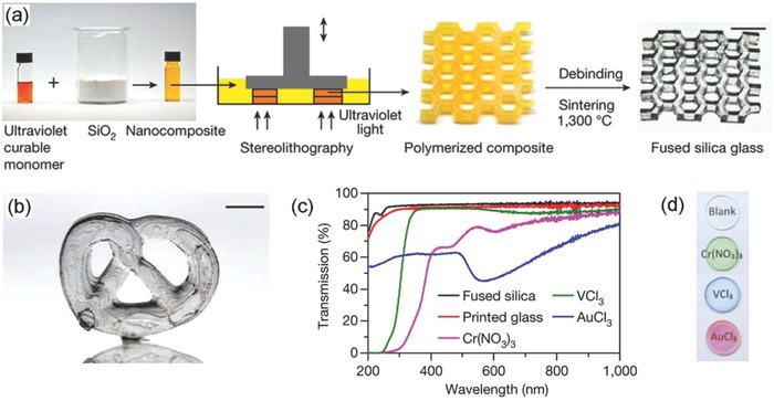
3D printed transparent glass. a) Schematics of the printing process of fused silica glass: first amorphous silica powder is mixed with an UV‐curable monomer, and the resulting nanocomposite resin is patterned by STL. The polymerized material is then converted in fused silica glass through debinding and sintering thermal treatments. Scale bar: 7 mm. b) Example of a 3D‐printed and sintered glass structure. Scale bar: 5 mm. c) UV–visible transmission spectrum of printed and sintered glass (black continuous line). The spectrum of commercial fused silica is shown for comparison. d) Example of colored fused silica glasses obtained upon doping with metal salts. Reproduced with permission.43 Copyright 2017, Macmillan Publishers Limited.
A major limit of laser STL, which is an intrinsically serial process, is in its low printing speed. Substantial variants have been introduced in this respect, to cure individual layers in a single step by projecting patterns onto the prepolymer instead of scanning by a laser beam. Projection is performed by using an UV‐illuminated digital system, such as a digital micromirror array device44, 45, 46 or a liquid‐crystal phase mask.47 The versatility of such approach, known as digital light processing (DLP) is exemplified in Figure 2 a–c, which displays a pH sensor printed on the surface of a tapered optical microfiber.46 The pattern is made of the ionic hydrogel, poly(acrylic acid) (PAA), which shows pH‐dependent swelling when immersed in solutions with pH in the range 2–7. Upon printing, the PAA micropads shrink, thus applying a periodic strain on the fiber and consequently coupling the fundamental guided mode and cladding modes by resonant scattering,46 which leads to a pH‐dependent dip in the fiber transmission spectra (Figure 2d). The sensors show reversible response, with characteristic time of about 102 s (Figure 2e).
Figure 2.

DLP‐printed pH optical sensor. a) Scheme of 3D printing system used to fabricate the PAA microstructures on the surface of an optical tapered fiber. b) pH‐sensing device. c) Optical microscopy image of a tapered optical fiber with a diameter of 30 µm. The insets c1, c2, and c3 show confocal microscopy images of PAA micropads printed on the fiber, with sizes: 325 × 100 µm2 (c1), 325 × 300 µm2 (c2) and 325 × 600 µm2 (c3). Insets in (c1–c3): photo of the devices. d) Reversible shift of the wavelength of the optical transmission dip versus pH. The inset shows the transmission spectra of the printed device at various values of pH. e) Dynamic response of the printed optical sensor (i.e., wavelength shift, left vertical scale) to different pH solutions (right vertical scale). Reproduced with permission.46 Copyright 2016, Wiley‐VCH.
Vertical growth rates for objects made by DLP can be speeded up to 1 m h−1 by inhibiting free‐radical polymerization through O2 diffusion,48 a method where almost continuous printing is achieved by letting a thin layer of uncured prepoly‐mer between the last polymerized layer and the transparent substrate through which light exposure occurs. This is accomplished by using an O2‐permeable substrate, by which the resin photopolymerization is locally inhibited, and a continuous renewal of reactive, liquid resin is obtained in the layer exposed to UV light.
The spatial resolution of laser STL and projection technologies is typically in the range 10–100 µm. Optical diffraction sets fundamental limits to the minimum size of a focused light beam and, consequently, to the in‐plane resolution, whereas the vertical resolution is limited by the capability of depositing very thin layers of prepolymers in between the exposure steps of consecutive slices. For UV light at 405 nm (currently used in commercially available laser STL 3D printers), the nominal, minimum spot size of a laser beam focused by low‐numerical aperture (NA) optics (NA < 0.1) is ≥2 µm, according to the Abbe relation. Another important aspect consists in the possibly anisotropic physical properties of structures printed layer‐by‐layer and with different in‐plane and vertical spatial resolutions.49 Little is known about the eventual anisotropy of the achieved optical properties. Instead, various studies are focused on methods for improving the characteristic pixelated and step‐case surface roughness, that is also detrimental for applications in optics. For instance, in‐plane roughness can be compensated by overexposure in STL, and by defocusing projected layer images in DLP. A new approach takes advantages of grayscale photo‐polymerization50 and meniscus equilibrium postcuring,51 improving significantly the finish of curved surfaces printed by DLP (achieved surface roughness < 7 nm), and allowing millimeter‐scale lenses to be obtained with imaging capability in line with standard optical components.52 Overall, spatial resolution and surface finishing remain issues, which are especially relevant for realizing optical components and devices operating at visible and near‐infrared (NIR) wavelengths. In this respect, other STL methods are being engineered, which rely on nonlinear optical absorption53 to improve the spatial resolution well below diffraction limits. Exploiting nonlinear absorption also allows the layer‐by‐layer concept to build objects to be overcome, enabling the continuous production of arbitrary 3D geometries.
2.2. Multiphoton Stereolithography
Multiphoton stereolithography (MP‐STL) is a laser‐based AM technique with resolution reaching a few tens of nanometers.54, 55, 56 When an ultrafast laser (pulse duration of tens or hundreds of femtoseconds) is focused inside the volume of a transparent, photosensitive material, the high intensity of the beam can induce multiphoton absorption within the focal voxel, causing local curing. Moving the beam along a continuous trajectory allows high‐resolution 3D structures to be obtained, in a free‐form manner and without the need to build the objects layer‐by‐layer. This significantly suppresses the presence of morphological or optical anisotropies between in‐plane and vertical directions. As a result, 3D objects with smooth surfaces can be realized,57 a property that makes MP‐STL particularly suitable for the fabrication of optical and optoelectronic components.
Like in any other lithographic technique, in order to recover the 3D pattern one needs to “develop” the sample, by immersing it into an appropriate solvent. However, MP‐STL has characteristic capabilities that no other technique can provide. On one hand, classic 3D printing such as STL cannot make structures with resolution better than a few micro‐meters, as mentioned above. On the other hand, high‐resolution methods such as electron‐beam lithography and focused ion beam can only pattern the surface layer of films; multiple layers and complex multistep depositions are required to fabricate anything resembling a 3D structure. The basic principles, challenges, and applications of MP‐STL are described extensively in several reviews and books and are beyond the scope of this progress report.58, 59, 60 Here, we will concentrate on the applications of MP‐STL in photonics, namely in the fabrication of micro‐optical elements and electromagnetic metamaterial structures.
Hybrid material technology deserves to be introduced in this framework, since this is prominent in MP‐STL addressing photonic applications. The first materials employed in MP‐STL were acrylate photopolymers and the high aspect ratio, negative photoresist SU‐8.61, 62, 63 However, the photonics community very quickly switched to using organic–inorganic hybrid materials prepared by sol–gel processes.64, 65, 66 These methods are based on the phase transformation of a sol of metallic oxide or alkoxide precursors to form a wet macromolecular hybrid network structure. The gel formed is subsequently reacted through MP‐STL to give a product similar to glass. The sol–gel technology provides a powerful tool for the development of optical materials by MP‐STL, as the resulting samples show high optical transparency and quality, postprocessing chemical and electrochemical inertness, and good mechanical and chemical stability. In addition, various functional compounds or nanosystems can be incorporated by employing guest–host or side chain–main chain strategies. Examples are metal alkoxides,67, 68 nonlinear optical molecules,69 QDs,70 and conducting ionogels and graphene.71 The most widely used hybrid materials are the silicate OrmoComp (and its different formulations) developed by the Fraunhofer Institute of Silicate Research72 and commercially supplied by Microresist Technology,73 and the zirconium silicate SZ2080.74, 75, 76, 77, 78 Examples of 3D components made by the latter material are shown in Figure 3 a,b.
Figure 3.
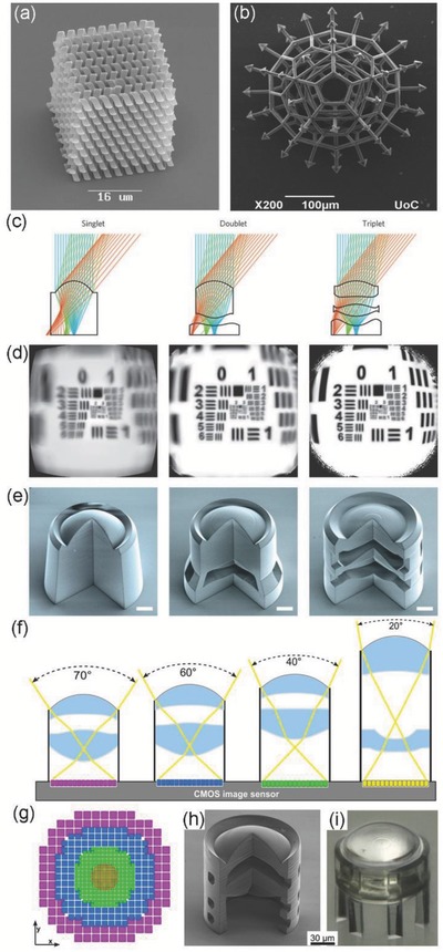
a) A photonic crystal and b) a complex concentric microstructure made using SZ2080. (a) Reproduced with permission.75 Copyright 2008, American Chemical Society. (b) Reproduced with permission.78 Copyright 2015, American Vacuum Society. c–e) Freestanding lens compound optical systems: (c) device schemes, (d) simulated images by using a USAF 1951 resolution test chart, (e) actual devices; scale bars: 20 µm. (c–e) Reproduced with permission.79 Copyright 2016, Macmillan Publishers Limited. f–i) A system of four different compound lenses on the same CMOS image sensor, combining different fields of view in one single system: (f) device schemes, (g) corresponding pixel size, evidencing an increased resolution toward the center of the image, (h, i) actual devices printed by MP‐STL. (f–i) Reproduced under the terms of the CC‐BY‐NC license.22 Copyright 2017, The Authors, some rights reserved; exclusive licensee American Association for the Advancement of Science.
Various miniaturized photonic structures have been developed by MP‐STL, taking advantage of the sub‐micrometer spatial resolution of the process and of the availability of materials with excellent transparency, as highlighted above. The obtained micro‐optical elements can be used for beam focusing and collimation, shaping, and imaging. For instance, MP‐STL is highly suitable for fabricating complex systems of lenses, as they can be made in a single step, without requiring further assembly.54 Freestanding compound optics, such as micro‐objective lenses (Figure 3c–e),79 pave the path for other relevant miniaturized systems such as endoscopes and microillumination elements. Compound optics can be even built directly on functional surfaces or devices as shown in Figure 3f–i, where lenses with different fields‐of‐view have been printed onto a single complementary metal–oxide–semiconductor (CMOS) sensor.22 Similarly, MP‐STL might be used to fabricate optical systems on fiber ends directly (Figure 4 a,b), eliminating also in this case the need for further assembly and consequent errors. There are optical fibers bearing ultra‐compact lens objectives (spherical, cylindrical, toric lenses) with numerous refractive surfaces,74, 79, 80 parabolic microreflectors,81 free‐form optical elements for donut and top‐hat beam shaping,82, 83 axicons,84 and sensors.85, 86
Figure 4.

a) A complex lens system on the end of an optical fiber. Scale bar: 25 µm. Reproduced under the terms of the CC‐BY license.82 Copyright 2016, The Authors. Published by Macmillan Publishers Limited. b) A fiber‐end Fabry–Perot gas microsensor, built directly on the top of a fiber. Reproduced with permission.86 Copyright 2015, IEEE. c–g) Examples of 3D metamaterial structures made using MP‐STL and selective electroless plating. (c)–(f) Reproduced with permission.98 Copyright 2017, Wiley‐VCH. (g) Reproduced with permission.99 Copyright 2015, American Chemical Society.
Another class of systems which can be manufactured by MP‐STL are metamaterials. These photonic elements do not exist in nature; their name derives from the Greek word “meta,” which means “beyond.” They are artificially engineered metallo‐dielectric structures whose electromagnetic properties are due to their architecture and not to the chemistry of their base components.87 In metamaterials, an assembly of structures can replace the role that atoms and molecules have in conventional materials, and elementary units are usually arranged in periodic patterns, at scales smaller than operating wavelengths. By appropriately designing and building metamaterial architectures, many new and unusual optical properties have been demonstrated such as negative refractive index, magnetism at optical frequencies, perfect absorption, and enhanced optical nonlinearities, in turn leading to original applications including ultrahigh‐resolution imaging, compact polarization optics, and cloaking devices.88, 89, 90, 91 However, the vast majority of materials printable with MP‐STL are dielectrics, so metal 3D metamaterials cannot be produced directly yet. There have been a few attempts employing multiphoton reduction of metals, but neither the achieved resolution nor the structural integrity was adequate.92, 93 The most common (and successful) approach to date is to make a dielectric scaffold using MP‐STL, and then cover it with silver or gold. The thickness of the metal layer should be thicker than the skin depth of the operating wavelength, so that the optical response of the structure is comparable to that of solid metals. To make metallic coats, electroless plating and chemical vapor deposition94, 95, 96 can be used. These techniques lack selectivity, leading to “blanket” metal deposition covering the substrate as well as the structures, which limits their application to reflective modes, or to bigger, freestanding structures. Infrared metamaterials can be also made using a positive photoresist and electroplating.97 In this case, a positive mold of the structure is made, which is filled with metal. Despite the excellent results, this method is not yet widely used, as accessible geometries are limited and the highest resolution achieved to date is of a few hundreds of nanometers. It is also possible to employ MP‐STL resins with metal‐binding sites, allowing metamaterial operation in transmission mode and much finer features to be obtained (Figure 4c–g).98, 99, 100
A few commercial MP‐STL systems are currently available, with typical in‐plane resolution of few hundreds of nanometers and vertical resolution of a few micrometers.101, 102, 103 Similarly to other AM technologies, one of the main issues is the time required to build a 3D object. The fabrication of a millimeter‐scale object with a resolution of a few hundreds of nanometers still requires building times of the order of days.52 New approaches are being developed aimed at achieving reasonable building times as well as sub‐micrometer feature size.104, 105, 106, 107
3. 3D Printing by Extrusion
The AM technologies which are based on light exposure provide the highest achievable spatial resolution, but they are limited by available photocurable compounds, a feature that restricts the possibility to build objects with heterogeneous parts and diverse composition. This issue is addressed by methods which rely on extrusion of materials, generally in form of continuous filaments through a nozzle, while 3D objects are still built by consecutively depositing many layers. Here, extrusion is promoted by either melting thermoplastic polymers as in fused deposition modeling (FDM), or applying a pressure to shear‐thinning viscous inks (as in direct writing methods). Extrusion technologies have enabled multimaterial printing, with resolution around hundreds of nanometers.108
In FDM, 3D plastic objects are generated by the deposition of polymer filaments.109, 110 A thermoplastic wire (polymethylmetacrylate (PMMA), polylactic acid (PLA), polysterene, polycarbonate, acrylonitrile butadiene styrene (ABS), etc.) is directed through a hot extrusion head, and the fused polymer is deposited in a continuous way, solidifying as soon as the filament temperature falls below the glass transition temperature. Typical extrusion temperatures are in the range 200–400 °C, depending on the melting behavior of the used polymer. Also the target substrate can be heated to ≈100 °C, in order to promote better adhesion between adjacent layers.
When building optical components, the main limit of FDM is in its spatial resolution (100–400 µm), which is largely determined by the size of the nozzle (0.1–0.4 mm). This might lead to quite rough surfaces and opaque printed structures, where coupling and propagation of UV, visible, and NIR light can be suppressed in a severe way. Nevertheless, FDM can be still exploited for optoelectronic device packaging.111 A relevant example is the fabrication of stretchable LEDs, realized by embedding liquid metal‐based electrical interconnects in printed, cylindrical hollow polymer structures. Such flexible systems can power LEDs even upon twisting of the polymer envelope up to 540°.111 Furthermore, FDM resolution would match values needed to realize components for use with terahertz and microwave radiation.112, 113 Compact terahertz laser sources114 are available which can be exploited as highly selective and noninvasive tools for environmental sensing and security. Hence, the field would significantly benefit from the development of specific methods to print windows, waveguides, lenses, and filters operating at terahertz frequencies. In this respect, issues are related to the absorption of most of the available polymers (e.g., ≥10 cm−1 for PLA at 0.5 THz).112 While attempts with high density polyethylene and polypropylene, which are transparent at terahertz frequencies, did not lead to satisfactory results, polystyrene turned out to be a suitable material in terms of both printability by FDM and low absorption losses (0.5 cm−1 at 0.5 THz).112 In addition, graded refractive index lenses for microwaves have been made by FDM of materials with different permittivity at 15 GHz (ABS possibly doped with 28% v:v SrTiO3 particles).113
3.1. Direct Ink Writing
Direct Ink Writing (DIW) relies on the controlled delivery of inks through a nozzle by an applied pressure.108 The ink then rapidly solidifies due to evaporation, phase changes, or gelation. The nozzle is mounted on a 3D translation stage, which moves along patterns defined by the object architecture and by its digital model. DIW allows single or multiple inks to be released in the form of filaments, and objects with well‐controlled shapes and composition to be created. Various parameters have to be accounted for during process engineering, related to the viscoelastic properties of the ink and to specific DIW variables.108, 115] Figure 5 a,b shows the typical rheology of DIW inks:116, 117 they must exhibit well‐defined viscoelasticity to flow through the nozzle while retaining shape upon deposition, and to feature shear thinning thus favoring extrusion. Viscoelasticity is particularly critical for avoiding collapse in structures suspended through a gap, such as freestanding dielectric waveguides with air cladding. The characteristic dependence of the ink elastic shear modulus (G′) on the shear stress is shown in Figure 5a: the rapid decrease of the shear modulus upon increasing the shear stress around values close to the shear yield is necessary for establishing a continuous flow through the nozzle upon applying a pressure, whereas G′ values above 104 Pa at low shear stress provide self‐supporting structures with superior stiffness.108 The insets of Figure 5a display examples of two gap‐spanning structures, imaged 1 h after production, highlighting a more stable shape for the structure printed from a stiffer ink. To fit with these rheological requirements, a compromise between high stiffness and moderate shear yield has to be found when formulating the composition of the ink. For instance, this can be accomplished by adding solid particles to the ink.116, 117 Figure 5b shows results for inks with different content of silica nanoparticles: a particle amount of 20 wt% leads to joining of the deposited filaments, creating a compact and monolithic structure with excellent optical transparency. Filaments extruded with slightly higher content of silica particles (23 wt%) can retain their gap‐spanning shape after extrusion but form an opaque structure. Therefore, the filamentary, layer‐by‐layer morphology of the printed elements can be controlled by tailoring the ink composition, with more uniform and homogeneous structures achieved by less viscous inks. The approach introduced in ref. 117 is very interesting, because in combination with postprinting thermal treatments it allows free‐form 3D glass components to be obtained, with optical properties (transparency and refractive index) well matching those of commercially available glasses.118
Figure 5.
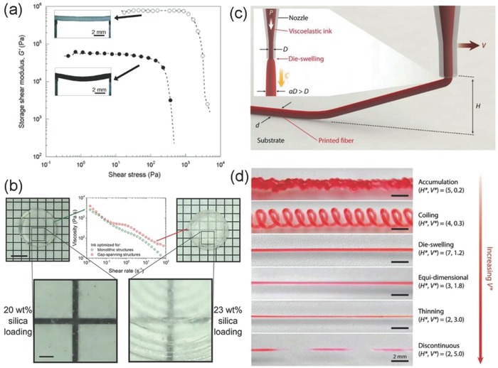
Material and process properties in DIW. a) Storage shear modulus, G′, versus applied shear stress for a fugitive ink filled with nanoparticles (fill circles) and for an organic ink doped with 40 wt% of microcrystalline wax (empty circles). The insets show optical images of corresponding suspended filaments (length 10 mm and diameter about 1 mm), acquired 1 h after printing. Reproduced with permission.116 Copyright 2005, Wiley‐VCH. b) Viscosity versus shear rate for two inks with 20 wt% (circles) and 23 wt% (squares) of silica nanoparticles. The photographs show the corresponding printed samples which have very different optical transparency. Low silica content favors fusion of printed filaments (left pictures), whereas increasing silica content allows stable gap‐spanning features, but leads to lower optical transparency (right pictures). Scale bar: 4 mm. Inset scale bar: 0.5 mm. Reproduced with permission.117 Copyright 2017, Wiley‐VCH. c) Schematic representation of a typical setup for 3D printing by DIW. d) Images of elementary structures printed by DIW for various process parameters, H* and V*, corresponding to the diverse printing modes. (c), (d) Reproduced with permission.115 Copyright 2018, Wiley‐VCH.
DIW can be applied to many other inks including concentrated polymers, viscous elastomers, fugitive organics, and filled epoxies,8, 108 with minimum feature size as low as 600 nm.119 Importantly, the process is carried out in ambient conditions, a feature relevant to preserve the optical properties of active components which can be embedded in the inks. Furthermore, the shear forces exerted during extrusion might induce an anisotropic arrangement of molecular constituents and of the embedded fillers, favoring their alignment along the length of the deposited filament. Recent experiments have highlighted a preferential alignment of elongated fillers (fibers, rods, and nanotubes) along the longitudinal axis of filaments, with resulting anisotropic swelling behavior and mechanical properties.120, 121 Additional work will be needed to investigate achieved optical properties (absorption, refractive index, photoluminescence, and light scattering), including their anisotropy (dichroism, birefringence, and polarization effects) in active or passive layers printed by DIW.
Figure 5c schematizes a few relevant printing parameters, such as the applied pressure, P, the nozzle inner diameter, D, and translation velocity, V, the ink extrusion speed, C, and filament diameter, d, and the working distance, H. Recently, Yuk and Zhao have developed an insightful model of the process, highlighting various DIW regimes characterized by different shapes of the deposited filaments.115 These regimes are summarized in Figure 5d, together with the corresponding adimensional parameters: H* = H/aD and V* = V/C, where a is the so‐called die swelling ratio which accounts for the broadening of the filament diameter upon printing (a > 1). For instance, upon increasing the nozzle velocity, one can obtain coiling structures, then continuous filaments with progressively decreasing diameter, and ultimately discontinuous structures (Figure 5d).115 This rich phenomenology can be highly relevant for 3D printing of photonic components, a potential not yet fully exploited.
The filamentary composition of materials printed by DIW is inherently well‐suited for the fabrication of optical waveguides. Figure 6 a–c shows exemplary top and cross‐sectional views of waveguides made of silk,122 a biopolymer with refractive index (n) 1.54 at visible wavelengths (633 nm), that can sustain light propagation when deposited on substrates with lower refractive index, such as glass (n = 1.52) or quartz (n = 1.48). These waveguides are fabricated by DIW with an ink composed of an aqueous silk‐fibroin solution (concentration 28–30 wt%), using a 5 µm glass nozzle immersed in a methanol‐rich reservoir, that induces filament solidification by favoring the transformation of amorphous random coils to stiff β‐sheets in the silk fibroin.122 Both straight and curved silk waveguides can be printed (Figure 6a,b), with smooth and defect‐free surface (inset of Figure 6b) and trapezoidal cross‐section (Figure 6c) due to a partial spread of the as‐deposited ink before complete solidification. The centimeter‐long silk waveguides can be coupled to a red laser, highlighting effective light transport (Figure 6d–f). Propagation losses are 0.81 dB cm−1 for wavy waveguides, and decrease to 0.25 dB cm−1 for straight structures.122 Being biocompatible, these printed components could be interfaced with living cells and integrated in implantable and biodegradable photonic devices.
Figure 6.
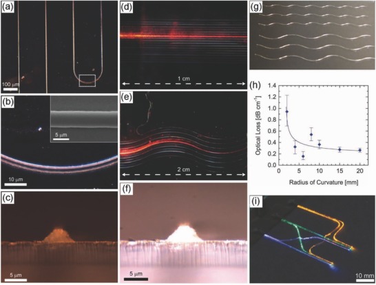
Waveguides printed by DIW. a) Optical microscopy image of printed silk waveguides. b) Higher magnification optical microscopy image of the curved region of the silk waveguide, as highlighted by a dashed box in (a). Inset: SEM image of the printed silk waveguide. c) Cross‐sectional optical image of a cleaved silk waveguide. d,e) Photographs showing diffused laser light coupled in straight (d) and curved (e) silk waveguides. f) Cross‐sectional view of light diffused by the cleaved surface of a silk waveguide. (a)–(f) Reproduced with permission.122 Copyright 2009, Wiley‐VCH. g) Photograph of curved waveguides made of OrmoClear. h) Optical propagation losses versus the radius of curvature of the waveguides. i) Photograph of a network of six OrmoClear waveguides with coupled LED light at three different colors. (g)–(i) Reproduced with permission.124 Copyright 2011, Wiley‐VCH.
The DIW printing head and nozzles can be modified to generate more complex structures,123 such as core–shell filaments.124 This is particularly advantageous for patterning compounds with poor viscoelasticity. Indeed, such materials can be embedded in the core of filaments, with a sacrificial shell featuring viscoelastic properties suitable for DIW. Following printing, suitable treatments can be carried out to solidify the core material while dissolving or removing the sacrificial shell. Figure 6g displays curved waveguides fabricated by printing a liquid core made of a photocurable resin (Ormoclear) with low absorption in the visible–NIR, in a shell from a viscoelastic aqueous solution of the triblock copolymer Pluronic F127. After printing and phopolymerization of the core resin, the shell is removed either by immersion in deionized water at room temperature, or by cooling at 5 °C and water rinsing.124 The curved waveguides exhibit optical losses ≤ 1 dB cm−1 for visible light, which decrease upon increasing the radius of curvature (Figure 6h), and they can be used to assemble printed photonic networks (Figure 6i).
Furthermore, photonic crystals can be obtained by DIW, as illustrated in Figure 7 a. Photonic crystals can be used in many device applications because of their high spectral selectivity, e.g., in spectral filters, high efficient reflectors, optical sensors, components for enhancing the radiative rate of embedded chromophores, and cavities for lasers.125 Polymeric and organic inks used for DIW often have relatively low refractive index (n = 1.5–1.8), which hardly leads to index contrast high enough to achieve good spectral selectivity. The refractive index of the printed structure can be enhanced, however, by either depositing high‐n materials on the surface of filaments (Figure 7b–d)126 or embedding high‐n particles in the inks (Figure 7e–h).127 In the first method, the printed item is used as a template for delivering other materials, such as Si and oxides, which also enhances mechanical stability. Figure 7b–d shows a photonic crystal realized by first printing a woodpile structure composed by rods with 1 µm diameter, spaced by 2.8 µm or 4.0 µm, and deposited from a concentrated polyelectrolyte ink.126 This structure is then coated by a 100 nm thick SiO2 layer. Afterward, the original organic template is removed by heating at 475 °C for 3 h. The resulting structure is composed by hollow SiO2 rods, which are finally coated by a 100 nm thick Si layer by chemical vapor deposition (Figure 7d). So‐produced samples feature a reflection peak at about 2 µm, in agreement with calculated spectra.126
Figure 7.

Photonic crystals by DIW. a) Scheme of a woodpile photonic crystal structure printed by DIW. b) SEM image of a Si/SiO2/Si hollow woodpile structure, realized by c) the multistep method schematized. d) SEM image of an individual hollow filament of the Si/SiO2/Si photonic crystal. (a)–(d) Reproduced with permission.126 Copyright 2006, Wiley‐VCH. e) A BaTiO3/PDMS nanocomposite 3D photonic crystal upon bending. f) Scheme of the variation of photonic crystal morphology under elongational stress. g,h) SEM images of 3D nanocomposite photonic crystals as viewed from the top (g) and in cross‐section (h). i) Measured transmission terahertz spectra of 3D nanocomposite photonic crystals, realized by printing inks with various BaTiO3 content. j) Transmission terahertz spectra of the 3D nanocomposite photonic crystals upon varying the relative elongation as schematized in (f). (e)–(j) Reproduced with permission.127 Copyright 2017, Wiley‐VCH.
The possibility of tuning the response of photonic crystals is frequently desired. In flexible photonic crystals, spectral properties can be tuned by applying elongational strains which modify the lattice geometry (Figure 7e,f). These crystals might be printed from a nanocomposite ink, made of an elastomer (polydimethylsiloxane, PDMS) and BaTiO3 nanoparticles added at various concentrations (10–40 wt%) to tailor refractive index as well as rheology.127 The printed hexagonal photonic crystals in Figure 7g,h have a bandgap around 0.4 THz, which can be shifted to lower frequencies by increasing the amount of loaded nanoparticles (Figure 7i). A redshift of the bandgap is also found upon elongation (Figure 7j), due to the varied spacing distances between the rods forming the crystal.127 This approach would allow the intensity of light signals reflected or transmitted by soft photonic crystals to be modulated upon stretching and releasing alternatively the printed structure.
Processing materials at ambient temperature and without using harsh chemicals, DIW is especially suitable for use with active optical compounds and light‐emitting organics. Figure 8 shows an interesting example of a fully printed optoelectronic device realized by DIW of multiple materials.128 This LED utilizes core–shell CdSe/ZnS QDs in its active layer, emitting green (550 nm) and orange (618 nm) light, and various other functional layers are printed in order to provide efficient charge injection and transport. More specifically, the printed QD LED encompasses a hole transport layer made of poly[N,N′‐bis(4‐butylphenyl)‐N,N′‐bis(phenyl)‐benzidine] (poly‐TPD), a transparent anode of poly(ethylenedioxythiophene):polystyrene sulfonate (PEDOT:PSS) surrounded by a ring of sintered Ag nanoparticles, which provides the necessary electrical contact, and a cathode made of eutectic gallium indium liquid metal (EGaIn). Different layers are deposited consecutively by DIW, through a selection of suitable orthogonal solvents.128 The printed devices exhibit turn on voltages of few Volts and maximum brightness of 250 cd m−2 at 5 V and 70 cd m−2 at 8 V for the green‐emitting and the orange‐emitting LEDs, respectively. Also important is the possibility to print the LEDs on curved substrates (Figure 8a–c). To this aim, a contact lens was first scanned (Figure 8b), and once digitalized, it was utilized as blueprint for optimizing the conformal morphology of the various LED layers. The QD LED printed on top of the contact lens (Figure 8c) features well‐behaved current–voltage characteristics and bright emission. By this approach, 3D‐printed optoelectronics (LEDs, photodetectors, photovoltaic components) could be integrated in complex and soft optical components (lenses, flexible biosensors, optical fibers) for medical applications, optogenetics, and components for augmented/virtual reality. Furthermore, as mentioned above, a key aspect of AM is in its capability of assembling many functional units in an interconnected and 3D fashion, well beyond standard planar architectures of optoelectronic boards and devices. Among other advantages, this would lead to artificial systems much more closely resembling biological functions. This is exemplified in Figure 8d–f, showing a matrix of 2 × 2 × 2 QD LEDs made by printing several different material in a unique DIW process.128 LEDs can be individually addressed in the 3D matrix (Figure 8g). Overall, this work has evidenced the unequalled potentialities of AM for photonics and optoelectronics, in terms of materials that can be combined in a single device, use of nonflat substrates, and truly 3D integration.
Figure 8.
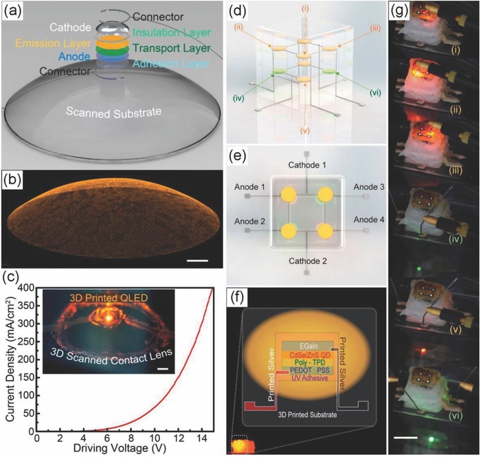
3D printed QD LEDs. a) 3D digital model of a QD LED to be printed on a curved substrate, whose scanned surface is shown in b). c) Current density versus the driving voltage of a QD LED printed on top of the surface of a contact lens. Inset: device image. Scale bar: 1 mm. d,e) Design of a 2 × 2 × 2 array of QD LEDs and of their electrical interconnects. f) Schematic illustration of the device architecture and of the layers of each QD LED component. g) Photographs of QD LED devices of the top layer (i)–(iii) and of the bottom layer (iv)–(vi). The letters (i)–(vi) highlight the assigned LED position in the 3D array, as illustrated in (d). Scale bar: 1 cm. Reproduced with permission.128 Copyright 2014, American Chemical Society.
3.2. Printing of Fibers by Electrospinning
The direct deposition of optical materials can be also performed by spinning viscoelastic polymer solutions by means of electrostatic fields. Electrospinning (ES)129, 130, 131, 132 utilizes an applied bias to stretch a polymer solution that is injected at a controlled flow rate through a metallic nozzle. When electrostatic forces are smaller than forces which stabilize the fluid body (viscoelasticity, surface tension), a pendant drop is formed at the nozzle and shaped into a Taylor cone. Upon increasing the applied voltage up to values high enough to overcome stabilizing forces, a continuous polymer jet is formed, which is elongated and stretched during its propagation from the nozzle to a second metallic element (collector). In the meanwhile, the solvent evaporates leading to the formation of solid and continuous filaments than can be deposited as individual fibers, as ordered 2D or 3D arrays, or as disordered networks (Figures 9 and 10 ).133, 134, 135, 136, 137 The main requirement for a successful ES process is having a sufficient amount of entanglements of the polymer chains in the spun solution (viscosities are in the range 10−1–103 Pa s), such to guarantee the formation of a continuous jet.138, 139
Figure 9.
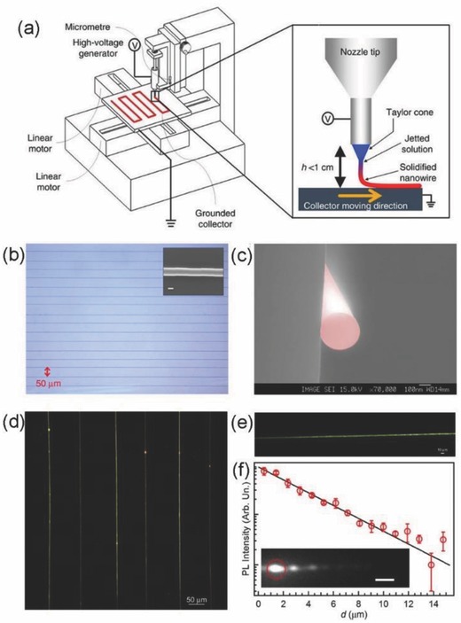
Direct printing by ES. a) Schematic illustration of a typical setup used for printing by ES. b) Optical microscopy image of an array of parallel printed filaments made by poly(9‐vinyl carbazole) (PVK). Inset: SEM image of a PVK filament. Scale bar: 200 nm. c) Cross‐sectional view of a PVK fiber imaged by SEM. (a)–(c) Reproduced with permission.133 Copyright 2013, Macmillan Publishers Limited. d,e) Confocal fluorescence microscopy image of an array of parallel filaments (d) and of a single fiber (e) made of MEH‐PPV/PEO. f) Plot of the fluorescence intensity transported through a printed fiber waveguide versus the distance, d, from the excitation spot. The continuous line is a fit to the data by an exponential decay function. Inset: fluorescence microscopy image of a MEH‐PPV/PEO fiber. The red circle highlights the excitation focused laser. Scale bar: 2 µm. (d)–(f) Reproduced under the terms of the CC‐BY license.134 Copyright 2013, The Authors. Published by The Royal Society of Chemistry.
Figure 10.
Examples of photonic devices made by ES. a) SEM image of a freestanding polymer waveguide doped with single QDs. b) Fluorescence image of a waveguide embedding an isolated QD, which is highlighted by a dashed box. c) Plot of the second order correlation function, g 2(t), measured by continuous wave laser excitation. The continuous line is a fit to the data by: g 2(t) ∼ 1 − (1/N)exp(|t|/τ), t is time and τ is the fluorescence decay time. The fit gives a value of g 2(t) = 0.1 at t = 0 delays, that is indicative of single photon emission. (a)–(c) Reproduced under the terms of the CC‐BY license.135 Copyright 2016, The Authors. Published by American Chemical Society. d–i) Examples of random laser devices. SEM images of an array of polycaprolactone (PCL) filaments (d) and of PCL filaments with silica nanoparticles deposited by biomineralization (g). Scale bars: 5 µm. The corresponding emission intensity maps and emission spectra, showing the variation of the photoluminescence as a function of the pumping fluence, are shown in (e), (f) and (h), (i), respectively. Insets in (e), (h): sample photographs. Scale bar: 5 mm. (d)–(i) Reproduced under the terms of the CC‐BY‐NC‐ND license.136 Copyright 2018, The Authors. Published by Wiley‐VCH. j) Bright light and k) UV‐excited emission photographs of an array of uniaxially aligned polymer filaments, doped with an UV dye. l–n) Photographs of emission from blue‐, green‐, and red‐emitting chromophores, respectively, in solutions excited by the UV light beam emitted by the array of polymer filaments. o) Images of the beam spot emitted by the polymer filaments at various distances, z, from the light source (top image: z = 0 mm, bottom image z = 1 mm). The beam divergence is 16.5 mrad. (j)–(o) Reproduced under the terms of the CC‐BY‐NC license.137 Copyright 2015, The Authors. Published by American Chemical Society.
The collector of fibers can be either static or dynamic, and either uniform or patterned. Disordered 3D networks of fibers are additively deposited on static and uniform collectors, whereas dynamic (rotating and translating collectors, or combination of them) or patterned target substrates140 allows ordered architectures to be manufactured. An important process parameter affecting the geometry achieved in deposited fibers is the distance between the nozzle and the collector. This aspect is strictly related to the complex dynamics of electrified jets.141 In fact, the jet trajectory is roughly straight only at short distance from the nozzle (typically, a few millimeters). At longer distances, oscillations of the spinneret, atmosphere turbulence, etc., can deviate the jet from a collinear configuration triggering the onset of large bending and whipping instabilities.141, 142, 143 As a consequence, two different ES approaches have been developed. In conventional ES,129, 130, 131 the collector is at large distance from the nozzle (many centimeters), and the jet instabilities prevent the precise positioning of individual filaments, which are instead collected as 3D, nonwoven mats of fibers. In the so‐called near‐field ES,132, 133 the initially stable, collinear jet is exploited, which is obtained by greatly reducing the nozzle–collector distance compared to the conventional method, and a scanning system is used to deposit the polymer in ordered 2D and 3D structures (Figure 9a). Overall, in ES, the order and morphology of the manufactured structures can be tuned by a proper choice of the process variables.
In addition, the very high strain rates applied to polymer jets (≥103 s−1) have two main effects: the first is a considerable decrease of the jet diameter upon increasing the distance from the nozzle, roughly following a power‐law relation139
| (1) |
where a is the polymer jet radius, a 0 is the initial radius, z stands for the axial coordinate, and κ is a constant of the order of unity. The length scale of the jet radius decrease is therefore z 0 (≈ 10−3 m), which is in turn related to the solution viscosity and conductivity, the applied flow rate, and the electric field. Solid state fibers with diameters down to 100 nm or less can be easily deposited, which are suitable for exploring phenomena occurring when light interacts with or propagates in subwavelength systems. The high strain rate also induces a preferential alignment of the polymer macromolecules along the jet, and then along the length of the deposited filaments,144 as found by polarized Raman spectroscopy,145 transmission electron microscopy,146 and scanning near‐field microscopy.147 This effect makes possible to obtain materials with highly anisotropic properties, such as optical dichroism and birefringence,146, 148 polarized emission,147, 149 and high charge mobility.150
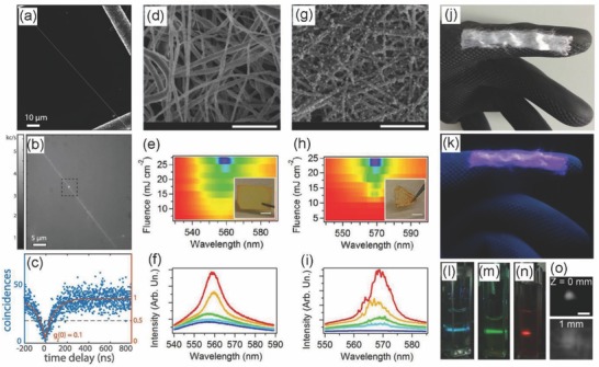
Figure 9b,c shows ordered electrospun filaments with circular cross‐section, made of conjugated polymers.133 Arrays of fibers can be also realized by light‐emitting polymers or blends, as in arrays obtained by near‐field ES of poly[2‐methoxy‐5‐(2‐ethylhexyl‐oxy)‐1,4‐phenylene‐vinylene] (MEH‐PPV) mixed with polyethylene oxide (PEO, Figure 9d,e).134 Similarly to waveguides printed by DIW, individual electrospun filaments transport light along their longitudinal axis, up to typical distances of tens of micrometers. When made with light‐emitting polymers, or doped with low‐molar‐mass chromophores or nanoparticles, electrospun fibers can guide photons emitted by the embedded sources, with propagation losses in the range 101–103 cm−1 (Figure 9f).134, 151 A recent application of these electrospun waveguides is in combination with single‐photon sources (Figure 10a–c).135 Here, single CdSeTe QDs are incorporated in polymer filaments, suspended across gaps to enhance confinement of light in the subwavelength fiber. The embedded QDs emit single photons with typical lifetime of 137 ns, which are coupled to the fundamental mode of the waveguide with efficiency up to 31%.135 Such hybrid systems are relevant for building 2D and 3D networks of quantum emitters, possibly interacting through arrays of polymer waveguides. Another application of electrospun optical materials, shown in Figure 10d–i, is based on mats of disordered, light‐scattering filaments in flexible random lasers.136 Here, an entirely additive method has been developed for the controlled fabrication of hybrid organosilica on top of electrospun fibers, by surface functionalization by silicatein and in vitro biosilicification. The comparison of the light scattering and random lasing properties of pristine electrospun fibers (Figure 10d–f) and of fibers decorated with silica particles (Figure 10g–i) evidences the onset of random lasing only in those samples where silica particles are grown with a specific spatial density.136 As a result, while pristine fibers can only support amplified spontaneous emission of a superimposed dye‐doped polymer layer (Figure 10e,f), the substrates with silica particles might exhibit random lasing modes (Figure 10h,i). Other devices for disordered photonics based on electrospun nanofibers exploit polymer filaments internally doped with either metallic152 or dielectric153 nanoparticles, as well as deterministic ring‐154 and cylindrical‐shaped155 lasing resonators with randomly distributed cavity sizes. Figure 10j shows an array of uniaxially aligned filaments of PMMA doped with an UV‐emitting dye. These flexible sources can be deposited conformally on nonplanar surfaces (Figure 10k).137 Upon optical excitation, the light emitted by the fibers can efficiently excite other fluorophores (Figure 10l–n), while propagating in free space with a divergence of 16.5 mrad (Figure 10o).137
Overall, ES turns out to be able to preserve the optical and electronic properties of organic materials and inorganic fillers. As a gentle AM process to realize 1D, 2D, and 3D photonic components with varied order, ES is enabling a novel range of nanowire‐based photonic devices where light emission, scattering, amplification, and transport can all be engineered.156, 157
4. Additive Fabrication by Material Jetting
Additive technologies which allow optoelectronic devices to be built with heterogeneous materials include methods based on jetting. Inkjet printing has been widely applied to realize optoelectronic devices with organic semiconductors158 or 2D materials.159 In inkjet printing processes, droplets are ejected through a nozzle on demand, by applying a suitable force (mechanical or electrical), and delivered onto on a substrate to define patterns.160, 161, 162 The ink must be properly engineered to lead to stable jetting, namely to produce single droplets without the formation of secondary fluid beads. To this aim, one can consider the inverse of the Ohnesorge number (Oh): , where D n is the nozzle diameter, and γ, ρ, η are the surface tension, density, and viscosity of the ink, respectively. Stable jetting is typically reported for 1 < Z O < 14.159, 160, 163 The morphology of deposited inks depends on their rheology, on the substrate wettability, on the properties of the printing apparatus, and on the applied external field. Various strategies allow such morphology to be directed with accuracy, including the suppression or the exploitation of coffee‐ring effects, the use of liquid substrates or of patterned solids, and the control of the extent of droplet coalescence.164 Since materials are deposited from solutions, the solvent evaporation is critically important to determine the ultimate morphology, crystallinity, and thickness uniformity of layers. These can be tailored, for instance, through in situ thermal treatments, by substrate heating. In combination with an optimized chemical formulation of the ink, such approach allows solar cells based on perovskites to be realized, showing power conversion efficiency up to 12.3%.165
The versatility of the inkjet technology in terms of solvents and chemical additives, which can be chosen to better preserve optoelectronic properties of active compounds, and the availability of commercial desktop printers, make this method widely used for the deposition of layers in photovoltaic devices,166, 167 visible and infrared photodetectors,163, 168, 169, 170, 171 rewritable structural color displays,172 saturable absorbers,163 luminescent patterns,168, 173 nanocavities,174 microring resonators,175 and microlasers.176 Interested readers are referred to outstanding reviews in the field.160, 161, 162, 177, 178 Structures realized by inkjet technique are mainly 2D. Interestingly, 3D optical components can be realized by the polyjet technology, combining inkjet printing of photocurable inks and local UV photopolymerization. Example of optical components realized by the polyjet method include 3D, mechanically tunable gyroid photonic crystals, and waveguides for terahertz radiation.179, 180
5. Other Solution‐Based and Hybrid Technologies
The variety of AM technologies is continuously increasing, and new methods or combinations of exposure‐ and extrusion‐based approaches are being developed to fulfill the demanding requirements of photonics and optoelectronics. These include techniques for 3D printing of glass, such as selective laser melting/sintering181 and binder jetting processes.182 The structures obtained in this way are often opaque, because of trapped bubbles that limit optical transparency by scattering of light. Recently, filament‐fed laser heating has been developed for 3D printing of transparent quartz and soda lime glass.183, 184 In this approach, a glass filament is continuously fed, locally heated by a focused CO2 laser, and once molten, it is deposited layer‐by‐layer. The use of a solid and continuously fed glass filament limits the formation and the entrapment of bubbles in the printed structures, improving significantly the transparency of the final objects.181 By this approach, quartz flat and curved components with transparency exceeding 90% (corresponding to an extinction coefficient of 13.2 m−1) are demonstrated upon surface polishing.184 In addition, refractive index has been measured in printed quartz windows and found to be homogeneous.184
A recently developed approach for the fabrication of 3D optical interconnects is the so‐called meniscus‐guided 3D writing, where the meniscus of a monomer or polymer solution is drawn by an atomic force microscope tip185 or by a micropipette186, 187 to form filamentary structures (Figure 11 a). This method is very effective for the fabrication of freestanding 3D waveguides (Figure 11b) with subwavelength diameter and low propagation losses (1–10 dB mm−1).187 The out‐of‐plane design allows optical losses due to light coupling into the substrate underneath to be greatly suppressed. Interestingly, stacked waveguides and optical interconnects can be printed with no contacts (Figure 11c), as well as interconnects spanning through gaps (Figure 11d) or over steps (Figure 11e). Figure 11f,g illustrates a potential application of meniscus‐guided 3D writing, that is printing of 3D, out‐of‐plane optical connections between nanostructured photon sources. Here a polystyrene waveguide (P1) is realized to bridge two ZnO nanorods (Z1 and Z2). Upon laser excitation, the printed waveguide transports light emitted by Z1 to Z2, with no coupling with the underlying substrate (Figure 11h). Freestanding multiterminal and branched optical interconnects can also be printed (Figure 11i,j), with complete merging and continuous connection between touching waveguides. By this method, optical splitters and multiplexers can be printed at high density, fully exploiting the volume out of the substrate plane.187
Figure 11.

3D optical waveguides. a) Schematics of the 3D printing process based on the stretching of the meniscus of a polymer solution. b) SEM image of a polystyrene 3D waveguide. Insets: zooms of the sample regions highlighted by the white and black box, respectively. c) SEM image of crossed 3D waveguides. The insets show magnified views of the crossing area. d,e) Examples of 3D waveguides printed through a gap (d) and a step (e). f) Schematic illustration of a 3D‐printed interconnect between ZnO nanorods. g) SEM image of a printed waveguide (P1) connecting two ZnO nanorods (Z1 and Z2) and h) corresponding fluorescence map, obtained by exciting the Z1 nanorod by a focused laser as schematized in (f). The fluorescence map evidences the optical coupling between Z1 and Z2 through P1, whereas no signal is observed from Z3. i) Schematics of a multibranched 3D optical interconnect. j) SEM image of a freestanding, multibranched, printed waveguide. The insets show a magnification of the branching point and of the area of coupling to nanoscale photon sources (NPSs), as highlighted by the white and black dashed boxes, respectively. Scale bars: 2 µm. Reproduced with permission.187 Copyright 2016, Wiley‐VCH.
A different approach for building 3D optical components is given by contact printing, where a suitable ink is transferred to a substrate by means of a rigid or elastomeric patterned mold. A relevant example is the well‐known microcontact printing,188 where the mold is inked with the material of interest (surface modifiers, organic molecules, proteins, etc.), and placed in conformal contact with a target substrate. The transfer of the ink to the target occurs in correspondence of the protruding features of the mold, provided that the interactions between the ink mole‐cules and the substrate are stronger than the adhesion between the ink and the mold. Elastomeric molds are typically used for the spatially selective delivery of molecules, which allows conformal contact with the target substrate to be easily obtained and elements to be fabricated by soft lithography at very low cost.188 Many substrates can be used, including metals, inorganic semiconductors, and oxides,188, 189 and printing can be carried out sequentially in a layer‐by‐layer fashion in order to build 3D structures.190 Interestingly, selective deposition of different molecules can be accomplished, using diverse inks simultaneously. Applications include printing of colloidal crystals and nanostructures for antireflection coatings,191 and bilayers of QD donor–acceptor systems with tight spatial control of the nonradiative energy transfer.192
The laser‐induced forward transfer (LIFT) is a noncontact 3D printing and assembly process, based on the transfer of a material from a transparent donor (carrier) to a receiving surface, as schematized in Figure 12 a.193, 194 The material to be transferred can be a highly viscous composite paste, a polymer film, a complex fluid, a metal oxide, a semiconductor, etc.,194, 195 whereas the shape of the elementary transferred building block (voxel) is determined by the spatial profile of the used laser, which can be changed in real‐time by using physical masks or spatial light modulators. Both the carrier and the receiving substrates can be translated along prescribed paths in order to print complex 2D or 3D structures (Figure 12b–e). In a typical LIFT process with a solid donor layer, above a threshold fluence the incident laser generates a gas pocket between the carrier and the donor film. During expansion, the stress at the edge of the irradiated area increases, and a mechanical fracture of the donor film takes place when its ultimate stress is surpassed. At this point, the delaminated area is propelled toward the receiving surface. Typical requirements for the donor film are therefore a high absorption coefficient at the incident laser wavelength and high mechanical resistance upon bending to avoid internal rupture of the irradiated area during the deflection caused by expansion of the gas.194, 196, 197 Microdisks of a positive photoresist (S1813) have been transferred onto flat and curved surfaces to form arrays of microlenses.196 To this aim, the microdisks have been heated up to their glass transition temperature, which allow the formation of plano‐convex microlenses through thermal reflow (Figure 12f–i). LIFT is highly versatile, allowing materials with diverse physicochemical properties to be assembled, and the geometries of the unitary building block to be varied during device building at variance with most AM methods, where the unitary building block is fixed by the laser spot size, the nozzle, or the printhead shape. LIFT can be also exploited for assembling fully functional optoelectronic devices, for instance, by printing interconnects on top of LEDs (Figure 12j–n).193 Polymer light‐emitting diode (PLED) pixels, with size 0.6 × 0.5 mm2, have been realized by using LIFT and a forward transfer process applied to a multilayer.197 The multilayer was composed by the Al cathode and the active layer (MEH‐PPV) of the devices, while the receiving surface was either indium tin oxide (ITO) or ITO coated with PEDOT:PSS.197 PLED pixels can be also fabricated by sequential LIFT applied to the active layer and the Al cathode.198 Other relevant examples of photonic devices made by LIFT include terahertz metamaterials, realized by forward laser printing of Ag split‐ring resonators on Si substrates.199
Figure 12.
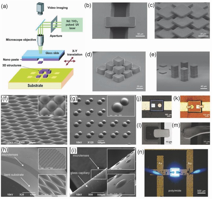
Laser‐induced forward transfer of optoelectronic and micro‐optical components. a) Scheme of the experimental setup for 3D printing by LIFT. b–e) SEM of various structures realized by 3D printing of voxels composed by a silver paste, and assembled to form a bridge on a Si channel (width 100 µm) (b), a multilayer scaffold (c), a pyramid (d), and high‐aspect ratio pillars (e). (a)–(e) Reproduced with permission.193 Copyright 2010, Wiley‐VCH. f–i) Examples of arrays of microlenses manufactured by laser transfer. SEM images of an array of closed‐packed microlenses (f), of periodically arranged dimers of microlenses (g), and of an array of lenses printed on the surface of a bent substrate (h) and of a glass capillary (i). (f)–(i) Reproduced with permission.196 Copyright 2018, Wiley‐VCH. j,k) Images of a LED embedded in a polyimide substrate before (j) and after (k) printing of the interconnects. l,m) SEM images of the printed interconnects. n) Image of the manufactured LED under operation. (j)–(n) Reproduced with permission.193 Copyright 2010, Wiley‐VCH.
The capability to manipulate fluids by micro‐ and nanofluidics is another route for the controlled delivery of materials with high precision. This can be done through networks or arrays of micrometric or sub‐micrometric channels, with interesting implications for building optical and photonic components additively. Examples include the fabrication of arrays of mesostructured optical waveguides with either straight or curved geometry, by using a patterned PDMS mold in conformal contact with a flat substrate.200 These channels can then be filled by sol–gel block copolymers placed at one of the open ends and penetrating by capillary flow. Full cross‐linking and consolidation of the silica network occur in about 12 h. After that time, the PDMS mold can be removed and an array of waveguides is formed. Upon doping with rhodamine and optical pumping, amplified spontaneous emission at 577 nm was observed from these systems.200 Microfluidics methods are especially effective for the fabrication of photonic components with anisotropic properties, because flows in channels can favor molecules in adopting an elongated, almost 1D conformation. Such molecular alignment has been observed for conjugated polymers flowing within channels with sub‐100 nm transversal size, and the resulting nanostructures have been found to feature anisotropic optical properties, namely to emit light polarized in a direction parallel to their length.201
Finally, it is worth mentioning that hybrid approaches combining microfluidics and UV and two‐photon photopolymerization have been developed for the continuous production of 3D fluorescent micro‐objects. These methods, known as continuous flow lithography,202, 203, 204 are schematized in Figure 13 a,b. A prepolymer doped with fluorescent particles or chromophores is cured locally by the use of a light beam during its flow through the channel. Either UV exposure through a mask (Figure 13a), or two‐photon polymerization (Figure 13b) can be used. The geometry of the printed micro‐objects can be changed in real time by shaping the light beam through a digital mirror device,205 instead of using fixed physical masks. 3D micro‐objects with complex shapes can be realized in this way, including fluorescent helical particles (Figure 13c,d) with surface roughness < 10 nm.204 In addition, various prepolymer solutions, featuring different emission wavelengths, can be combined in a microchannel where the laminar coflow provides sharp interfaces between them due to poor, diffusion‐limited mixing.206 By photopolymerization across the interface of coflowing solutions, 3D particles with various encoded optical patterns can be realized (inset of Figure 13a).203 For instance, lanthanide ion nanocrystals, featuring distinct, visible light emission by upconversion upon NIR optical pumping, have been incorporated in such particles. The resulting large anti‐Stokes shifts leads to straightforward spectral separation and minimal interference with the excitation radiation, and improved signal‐to‐noise ratios.203 Figure 13e shows an example of application of these microparticles as anticounterfeiting barcodes, which can be embedded in pharmaceutical packages, banknotes, credit cards, ceramic objects, artworks, and high‐temperature cast items made of poly‐styrene (top panels in Figure 13e). The particles can be easily imaged with a smartphone and a 20× objective. In absence of NIR excitation, no fluorescence signal is detected (lower panels in Figure 13e), whereas bright, NIR‐excited luminescence (middle panels) allows the identification of the embedded barcodes unambiguously.
Figure 13.

3D light‐emitting microparticles. a) Schematic diagram of a continuous flow lithography system, utilizing multiple coflows of monomers with lanthanide‐doped fluorescent nanoparticles. The inset shows fluorescence images of various manufactured particles. Reproduced with permission.203 Copyright 2014, Macmillan Publishers Limited. b) Schematics of two‐photon continuous lithography. c) Bright field optical microscopy image of a 3D helical particle made by two‐photon continuous flow lithography. d) The corresponding fluorescence microscopy image is shown. (b)–(d) Reproduced with permission.204 Copyright 2012, Wiley‐VCH. e) Fluorescent microparticles as encoded barcodes in anticounterfeiting. The imaging system utilized a portable detector (Apple iPhone 4S with a 20× objective), as shown in the left image. The particles were embedded in various objects as shown in the top panels (from left to right: blister packs, banknotes, credit cards, curved ceramic objects, artwork, and high‐temperature‐cast polystyrene objects). The middle and bottom panels show the corresponding acquired images upon excitation with a 980 nm laser (excitation power: 1W) and without laser excitation, respectively. Reproduced with permission.203 Copyright 2014, Macmillan Publishers Limited.
6. Conclusion and Outlook
AM technologies are introducing new design and production rules for both passive and active optical materials, for the fabrication of photonic and optoelectronic devices, and for the interwoven integration of photonic components. The progress of this field is supported by the continuous expansion of the range of materials that can be processed, by the introduction of new fabrication methods, and by the improvement in the achievable spatial resolution, as summarized in Table 1 . The variety of 3D‐printable optical materials, and the possibility to shape them across many lengthscales (from hundreds of nanometers to centimeters) are enabling the design of photonic devices (such as photonics crystals and waveguides) with frequency response ranging from the visible to terahertz and microwave. Recent relevant breakthroughs include the possibility of printing glass‐based components, with transparency, thermal and mechanical resistance comparable to commercially available glass.43, 117, 118, 183, 184 Fully 3D printed LEDs have also been demonstrated, by intriguing approaches for manufacturing the various needed layers, as well as photonic devices conformable to complex, nonplanar surfaces.128 Combination of different technologies turns out to be a valid route for multimaterial processing, and for high‐throughput production of 3D objects with calibrated optical properties. Currently, fluorescent 3D microparticles can be produced at a rate of 104–105 particles h−1,203, 206 by a combination of microfluidics and either UV or two‐photon photopolymerization.
Table 1.
Additive technologies developed for manufacturing of photonic and optoelectronic components
| Additive technology | Commercial printers available | Building volumea) [cm3] | Feature size [µm] | Printing speeda) [mm s−1] | Optical/electronic material demonstrated | Multimaterial capability | Demonstrated photonic and optoelectronic devices |
|---|---|---|---|---|---|---|---|
| Laser stereolithography | Yes | 103–106 | 10–100a) | – | Acrylates, epoxies, nanocomposites | No | Optical windows |
| Digital light processing | Yes | 102–104 | 30–100a) | – | Acrylates, glassesb) | No | Lenses, optical windows, optical sensors |
| Continuous digital light processing | Yes | 102–103 | 30–100a) | 0.03 | Acrylates | No | – |
| Multiphoton stereolithography | Yes | 3 × 10⁻⁵–3 × 10² | 0.2–10a) | 0.1–10 | Acrylates, epoxides, nanocomposites | No | Microlenses, optical sensors, photonic crystals, waveguides, metamaterials |
| Fused deposition modeling | Yes | 103–106 | 100–500a) | 10–103 | Thermoplastic polymers, nanocomposites | Yes | Microwave and terahertz lenses |
| Direct ink writing | Yes | 102–103 | 10–100a) | 0.1–102 | Glasses,b) acrylates, epoxies, silk, elastomers, nanocomposites, conjugated polymers, conductive inks | Yes | Waveguides, photonic crystals, LEDs, optical windows |
| Electrospinning | Yes | 1–102 | 0.1–1a) | 1 | Thermoplastic polymers, conjugated polymers, nanocomposites | Yes | Waveguides, single‐photon sources, optical amplifiers, optical sensors, lasers |
| Inkjet | Yes | Typical printing area 102 cm2 | 20–80a) | – | Conjugated polymers, conductive inks, perovskites, block copolymers, 2D materials | Yes | Photodiodes, solar cells, organic LED, saturable absorbers, optical resonators, lasers, color displays |
| Polyjet | Yes | 104 | 16–30a) | – | Acrylates | Yes | Waveguides, photonic crystals |
| Filament‐fed laser heating process | No | – | 300c) | – | Glasses | No | Optical windows |
| Meniscus‐guided 3D writing | No | – | 0.1–1d) | – | Thermoplastic polymers | No | Waveguides |
| Microcontact printing | Yes | Typical printing area 102 cm2 | 0.05a) | – | Quantum dots, colloids, proteins | Yes | Luminescent patterns |
| Laser‐induced forward transfer | No | – | 0.5–10e) | – | Photoresists, conductive pastes, conjugated polymers | Yes | Microlenses, metal contacts, terahertz metamaterials, polymer LEDs |
| Micro‐ and nanofluidics | No | – | 0.07f) | – | Conjugated polymers, sol–gel, block copolymers | Yes | Waveguides, lasers |
| Continuous flow lithography | No | – | 0.4g) | – | Acrylates, nanocomposites | Yes | Luminescent microparticles, barcodes |
Despite such progress, some challenges are still open, as highlighted in Table 2 , and AM technologies for photonics and optoelectronics still remain matter of research rather than production tools. To move from laboratories to factories, first throughput has to be improved. For instance, while achieving high spatial resolution and good surface finishing, multiphoton processes proceed by scanning point by point in an individual layer, building up the 3D shape a single layer at a time.207 The efficiency of this process depends on the laser power available, the speed of the scanning system, and also the photopolymer. Since the technological opportunities opened by MP‐STL are unique, a lot of research is currently focused on the improvement of its throughput by developing more efficient photoinitiators, as well as higher power lasers and faster motion systems. In addition, efforts are devoted to improve the throughput of the technique by developing high aspect ratio MP‐STL,104 by using multiple beams,105, 106 and by moving toward holographic MP‐STL.107 Other issues to be addressed in the near future are those associated with i) multiscale printing, ii) multimaterial processing, and iii) multidimensional integration of optoelectronic and photonic devices.
Table 2.
Main challenges of AM technologies for fabrication of photonic and optoelectronic devices
| Additive technology | Optical properties | Spatial resolution | Interface uniformity | Uniformity of structure |
|---|---|---|---|---|
| Laser stereolithography | Postprocessing treatment needed | Low | – | Rough surface and postprocessing treatment needed |
| Digital light processing | Postprocessing treatment needed | Low | – | Rough surface and postprocessing treatment needed |
| Continuous digital light processing | – | Satisfactory | – | Smooth surfaces |
| Multiphoton stereolithography | Homogeneous optical properties of printed structures | Good | Satisfactory for components with heterogeneous materials | Smooth surfaces |
| Fused deposition modeling | Postprocessing treatment needed | Low | – | Rough surface and postprocessing treatment needed |
| Direct ink writing | Properties of pristine materials preserved | Satisfactory | Printing of functional multimaterials in individual devices demonstrated | Tailorable upon control of process variables |
| Electrospinning | Anisotropy of optical properties observed | Satisfactory | Satisfactory for multimaterial processing | Tailorable upon control of process variables |
| Inkjet | Properties of pristine materials preserved | Low | In situ and/or postprocessing annealing needed | Tailorable upon control of process variables |
| Polyjet | Properties of pristine materials preserved | Low | Satisfactory for components with heterogeneous materials | Tailorable upon control of process variables |
| Filament‐fed laser heating process | Homogeneous optical properties of printed structures | Low | – | Rough surface and postprocessing treatment needed |
| Meniscus‐guided 3D writing | Properties of pristine materials preserved | Good | Satisfactory for components with heterogeneous materials | Smooth surfaces |
| Microcontact printing | Properties of pristine materials preserved | Good | Satisfactory for components with heterogeneous materials | Smooth surfaces |
| Laser‐induced forward transfer | Properties of pristine materials preserved | Low | Postprocessing annealing needed | Smooth surfaces after postprocessing treatment |
| Micro‐ and nanofluidics | Anisotropy of optical properties observed | Good | Satisfactory for components with heterogeneous materials | Smooth surfaces |
| Continuous flow lithography | Properties of pristine materials preserved | Good | Sharp interfaces | Smooth surfaces |
Multiscale Printing: Photonics and optoelectronics have stringent requirements in terms of minimum size of the device features and they are currently fully accessible only by MP‐STL. At the same time, most of optical systems include components with macroscale size, thus needing AM technologies which can shape materials at different spatial scales. The resolution achieved nowadays by MP‐STL is at the nanometer scale, mainly due to techniques employing radical depletion, the highest resolution reported is an impressive 9 nm.56 However, this is done using high NA, oil‐immersed objectives with working distance below 200 µm, limiting both the area that can be patterned and the height of the structures to be built. This issue has been partly addressed by techniques such as “dip‐in” lithography208 or MP‐STL with wider objective working range (WOW),104 where the objective is immersed inside a liquid photoresist, making the working distance irrelevant. However, these techniques have their drawbacks: dip‐in lithography requires that the photopolymer refractive index matches the n value of the objective, limiting dramatically the materials that can be used. This is particularly important when the desired structures need to have a specific bulk functionality, such as nonlinearity or metal affinity. WOW MP‐STL, which uses a sealed oil‐immersed objective, can be used only with liquid resists, while the majority of materials used in photonics and optoelectronics are gels.64 Other pulse‐shaping techniques have produced high aspect ratio structures with adequate resolution.209 Recently, a new method employing simultaneous spatiotemporal focusing of femtosecond laser pulses has been used to make centimeter‐scale structures with 10 µm resolution.210 The fabrication of macroscale structures with sub‐micrometer resolution using materials with specific functionality remains elusive. Conversely, macroscale systems can be built by other AM approaches, tough with poor resolution, often not suitable for optical applications. One can image that in the future novel methodologies or combinations of current AM processes will be conceived, hopefully with integrated in situ process‐sensing elements,211 which will allow macroscale optical components with high spatial precision and uniformity to be realized. In this respect, a paradigm shift is probably necessary, more specifically methods no more based on the layer‐by‐layer approach, but instead based on continuous printing such as the continuous liquid interface production48 and the continuous flow lithographies.202, 204 While enhancing the printing speed, continuous processes have been demonstrated to be effective in improving the surface roughness of the manufactured objects, down to tens of nanometers.204
Multimaterial Processing: Simultaneous processing of diverse materials is of paramount relevance in photonics and optolectronics, where metal contacts, semiconducting active layers, transparent windows or waveguides, and dielectric or metal mirrors have to be frequently combined in complex systems. While DIW can currently manage different materials in a unique process,128 research efforts are still required in order to develop inks with advanced optoelectronic properties, such as optical gain, optical nonlinearity, efficient light‐to‐current (and current‐to‐light) conversion. For exposure‐based printing processes, the route is harder to some extent, because these methods can normally process one material at a time (typically passive and with limited optical functionality). Printed materials with graded composition and optical properties are still lacking. All such issues are critical for the future development of environmentally responsive optical systems, namely adaptive components which can self‐tune their properties in response to external stimuli.120, 212, 213
Multidimensional System Integration: Photonics and optoelectronics have been traditionally developed in planar configurations, with unavoidable limitations in terms of device architecture and density. AM technologies can potentially extend optoelectronic systems out of plane, but little has been done in this direction so far. This requires new design rules for single devices, as well as for their interconnects. Fully 3D waveguides with bent geometries can in principle lead to a more efficient connection of multiple optically active elements.187
Overall, there is already a lot of work on employing AM in a variety of photonic and optoelectronic applications, and the main challenge remains to move from prototyping to production. One of the most exciting areas in research is related to architected materials with targeted optical properties, that are defined by material architecture and not by material chemistry or composition. These systems defy common associations, such as mechanical strength and density, or optical absorption and bandgap. Photonic crystals and electromagnetic metamaterials presented above are only a small part of the current revolution in architected materials. More efforts can be done in this direction, as currently being pursued in metamaterials with targeted mechanical properties.214, 215, 216, 217, 218, 219 There are still numerous opportunities for enhancing the properties and interconnectivity of optoelectronic devices, by exploring novel, fully 3D architectures and AM of optically active materials.
Conflict of Interest
The authors declare no conflict of interest.
Acknowledgements
A.C., L.P., and D.P. acknowledge the European Research Council (ERC) for financial support under the European Union's Horizon 2020 research and innovation programme (grant agreement No. 682157, “xPRINT”). M.F. acknowledges financial support from the ERA.Net RUS Plus project “EXODIAGNOS” – RUSPLUS_INNO_FULL‐110.
Biographies
Andrea Camposeo, PhD in Physics (University of Pisa), is senior researcher at the Nanoscience Institute of the CNR. He has been visiting scientist at the University of Bonn, Toronto, Harvard, FORTH, and St. Andrews. His research activities include the development of optically active micro‐ and nanostructures by electrospinning and 3D printing for photonic applications and the investigation of the optical properties of light‐emitting polymers, composites, nanofibers, and of organic‐based light‐emitting devices. He is the recipient of the xPRINT Grant from the European Research Council.

Luana Persano, PhD in Innovative Materials and Technologies, is staff researcher at the Nanoscience Institute of the CNR. She has been Marie‐Curie fellow at the FORTH, Greece, and visiting scientist at the Harvard University and at the University of Illinois. Her research interests include nanomanufacturing and lithographic processes onto nanocomposites and active materials in the form of films, nanoparticles, and fibers, and the implementation of nanophotonic and piezoelectric devices based on them.

Maria Farsari is Research Director at the IESL‐FORTH, where she joined in 2003. Her main research interests are multiphoton lithography, laser‐based nanofabrication, and material processing using ultrafast lasers. She received her first degree from the University of Crete and her PhD from the University of Durham, UK. The subject of her PhD was organic nonlinear optics. After graduating, she worked as a postdoctoral research fellow at the Universities of Durham and Sussex and as a Senior Optical Scientist for the security company DeLaRue Holographics. She is a founding member of Xsil Ltd.

Camposeo A., Persano L., Farsari M., Pisignano D., Advanced Optical Materials 2019, 7, 1800419 10.1002/adom.201800419
Contributor Information
Andrea Camposeo, Email: andrea.camposeo@nano.cnr.it.
Luana Persano, Email: luana.persano@nano.cnr.it.
Maria Farsari, Email: mfarsari@iesl.forth.gr.
Dario Pisignano, Email: dario.pisignano@unipi.it.
References
- 1. ISO/ASTM Standard 52900 , Standard Terminology for Additive Manufacturing – General Principles – Part 1: Terminology, ISO/ASTM International, Switzerland: 2015. [Google Scholar]
- 2. Bourell D. L., Annu. Rev. Mater. Res. 2016, 46, 1. [Google Scholar]
- 3. Ligon S. C., Liska R., Stampfl J., Gurr M., Mülhaupt R., Chem. Rev. 2017, 117, 10212. [DOI] [PMC free article] [PubMed] [Google Scholar]
- 4. Martin J. H., Yahata B. D., Hundley J. M., Mayer J. A., Schaedler T. A., Pollock T. M., Nature 2017, 549, 365. [DOI] [PubMed] [Google Scholar]
- 5. Hirt L., Reiser A., Spolenak R., Zambelli T., Adv. Mater. 2017, 29, 1604211. [DOI] [PubMed] [Google Scholar]
- 6. Eckel Z. C., Zhou C., Martin J. H., Jacobsen A. J., Carter W. B., Schaedler T. A., Science 2016, 351, 58. [DOI] [PubMed] [Google Scholar]
- 7. Farahani R. D., Dubé M., Therriault D., Adv. Mater. 2016, 28, 5794. [DOI] [PubMed] [Google Scholar]
- 8. Truby R. L., Lewis J. A., Nature 2016, 540, 371. [DOI] [PubMed] [Google Scholar]
- 9. Klippstein H., De Cerio Sanchez A. D., Hassanin H., Zweiri Y., Seneviratne L., Adv. Eng. Mater. 2018, 20, 1700552. [Google Scholar]
- 10. Gu D. D., Meiners W., Wissembach K., Poprawe M., Int. Mater. Rev. 2012, 57, 133. [Google Scholar]
- 11. Melchels F. P. W., Domingos M. A. N., Klein T. J., Malda J., Bartolo P. J., Hutmacher D. W., Prog. Polym. Sci. 2012, 37, 1079. [Google Scholar]
- 12. Murphy S. V., Atala A., Nat. Biotechnol. 2012, 32, 773. [DOI] [PubMed] [Google Scholar]
- 13. Waheed S., Cabot J. M., Macdonald N. P., Lewis T., Guijt R. M., Paull B., Breadmore M. C., Lab Chip 2016, 16, 1993. [DOI] [PubMed] [Google Scholar]
- 14. Au A. K., Huynh W., Horowitz L. F., Folch A., Angew. Chem., Int. Ed. 2016, 55, 3862. [DOI] [PMC free article] [PubMed] [Google Scholar]
- 15. Zhang F., Wei M., Viswanathan V. V., Swart B., Shao Y., Wu G., Zhou C., Nano Energy 2017, 40, 418. [Google Scholar]
- 16. Stevens A. G., Oliver C. R., Kirchmeyer M., Wu J., Chin L., Polsen E. S., Archer C., Boyle C., Garber J., Hart A. J., 3D Print. Addit. Manuf. 2016, 3, 226. [DOI] [PMC free article] [PubMed] [Google Scholar]
- 17. Schünemann S., Brittman S., Chen K., Garnett E. C., Tüysüz H., ACS Photonics 2017, 4, 2522. [Google Scholar]
- 18. Liu N., Guo H., Fu L., Kaiser S., Schweizer H., Giessen H., Nat. Mater. 2008, 7, 31. [DOI] [PubMed] [Google Scholar]
- 19. Crespi A., Osellame R., Ramponi R., Brod D. J., Galvão E. F., Spagnolo N., Vitelli C., Maiorino E., Mataloni P., Sciarrino F., Nat. Photonics 2013, 7, 545. [Google Scholar]
- 20. Spagnolo N., Vitelli C., Aparo L., Mataloni P., Sciarrino F., Crespi A., Ramponi R., Osellame R., Nat. Commun. 2013, 4, 1606. [DOI] [PubMed] [Google Scholar]
- 21. Zhang F., Niu S., Guo W., Zhu G., Liu Y., Zhang X., Wang Z. L., ACS Nano 2013, 7, 4537. [DOI] [PubMed] [Google Scholar]
- 22. Thiele S., Arzenbacher K., Gissibl T., Giessen H., Herkommer A. M., Sci. Adv. 2017, 3, e1602655. [DOI] [PMC free article] [PubMed] [Google Scholar]
- 23. Kim D.‐H., Lu N., Ghaffari R., Kim Y.‐S., Lee S. P., Xu L., Wu J., Kim R.‐H., Song J., Liu Z., Viventi J., de Graff B., Elolampi B., Mansour M., Slepian M. J., Hwang S., Moss J. D., Won S.‐M., Huang Y., Litt B., Rogers J. A., Nat. Mater. 2011, 10, 316. [DOI] [PMC free article] [PubMed] [Google Scholar]
- 24. Kim R.‐H., Kim D.‐H., Xiao J., Kim B. H., Park S.‐I., Panilaitis B., Ghaffari R., Yao J., Li M., Liu Z., Malyarchuk V., Kim D. G., Le A.‐P., Nuzzo R. G., Kaplan D. L., Omenetto F. G., Huang Y., Kang Z., Rogers J. A., Nat. Mater. 2010, 9, 929. [DOI] [PubMed] [Google Scholar]
- 25. Kim J., Kim M., Lee M.‐S., Kim K., Ji S., Kim Y.‐T., Park J., Na K., Bae K.‐H., Kim H. K., Bien F., Lee C. Y., Park J.‐U., Nat. Commun. 2017, 8, 14997. [DOI] [PMC free article] [PubMed] [Google Scholar]
- 26. Kim T.‐I., McCall J. G., Jung Y. H., Huang X., Siuda E. R., Li Y., Song J., Song Y. M., Pao H. A., Kim R.‐H., Lu C., Lee S. D., Song I.‐S., Shin G., Al‐Hasani R., Kim S., Tan M. P., Huang Y., Omenetto F. G., Rogers J. A., Bruchas M. R., Science 2013, 340, 211. [DOI] [PMC free article] [PubMed] [Google Scholar]
- 27. Yang T., Xie D., Li Z., Zhu H., Mater. Sci. Eng., R 2017, 115, 1. [Google Scholar]
- 28. Huang Y., He Z., Wu S.‐T., Opt. Express 2017, 25, 32757. [Google Scholar]
- 29. Lee Y.‐H., Yin K., Wu S.‐T., Opt. Express 2017, 25, 27008. [DOI] [PubMed] [Google Scholar]
- 30. O'Carroll D., Lieberwirth I., Redmond G., Small 2007, 3, 1178. [DOI] [PubMed] [Google Scholar]
- 31. Papadimitrakopoulos F., Konstadinidis K., Miller T. M., Opila R., Chandross E. A., Galvin M. E., Chem. Mater. 1994, 6, 1563. [Google Scholar]
- 32. Kulkarni A. P., Kong X., Jenekhe S. A., J. Phys. Chem. B 2004, 108, 8689. [Google Scholar]
- 33. Favre A., Lee E., Apostolopoulos V., Gawith C. B. E., Tai C.‐Y., Taylor E., Kondo Y., Koizumi F., Opt. Mater. 2004, 27, 7. [Google Scholar]
- 34. Chen J., Wu Y., Li X., Cao F., Gu Y., Liu K., Liu X., Dong Y., Ji J., Zeng H., Adv. Mater. Technol. 2017, 2, 1700132. [Google Scholar]
- 35. Hull C. W. (UVP, Inc.), U. S. Patent 4575330, 1986.
- 36. Chen M., Zhong M. J., Johnson J. A., Chem. Rev. 2016, 116, 10167. [DOI] [PubMed] [Google Scholar]
- 37. Pan X., Tasdelen M. A., Laun J., Junkers T., Yag Y., Matyjaszewski K., Prog. Polym. Sci. 2016, 62, 73. [Google Scholar]
- 38. Shi S., Croutxé‐Barghorn C., Allonas X., Prog. Polym. Sci. 2017, 65, 1. [Google Scholar]
- 39. Melchels F. P. W., Feijen J., Grijpma D. W., Biomaterials 2010, 31, 6121. [DOI] [PubMed] [Google Scholar]
- 40. Reddy C. S., Arinstein A., Zussman E., Polym. Chem. 2011, 2, 835. [Google Scholar]
- 41. Gurr M., Hofmann D., Ehm M., Thomann Y., Kübler R., Mülhaupt R., Adv. Funct. Mater. 2008, 18, 2390. [Google Scholar]
- 42. Barichard A., Galstian T., Israëli Y., J. Phys. Chem. B 2010, 114, 14807. [DOI] [PubMed] [Google Scholar]
- 43. Kotz F., Arnold K., Bauer W., Schild D., Keller N., Sachsenheimer K., Nargang T. M., Richter C., Helmer D., Rapp B. E., Nature 2017, 544, 337. [DOI] [PubMed] [Google Scholar]
- 44. Sun C., Fang N., Wu D. M., Zhang X., Sens. Actuators A 2005, 121, 113. [Google Scholar]
- 45. Zhou F., Cao W., Dong B., Reissman T., Zhang W., Sun C., Adv. Opt. Mater. 2016, 4, 1034. [Google Scholar]
- 46. Yin M.‐J., Yao M., Gao S., Zhang A. P., Tam H.‐Y., Wai P.‐K. A., Adv. Mater. 2016, 28, 1394. [DOI] [PubMed] [Google Scholar]
- 47. Zheng X., Deotte J., Alonso M. P., Farquar G. R., Weisgraber T. H., Gemberling S., Lee H., Fang N., Spadaccini C. M., Rev. Sci. Instrum. 2012, 83, 125001. [DOI] [PubMed] [Google Scholar]
- 48. Tumbleston J. R., Shirvanyants D., Ermoshkin N., Janusziewicz R., Johnson A. R., Kelly D., Chen K., Pinschmidt R., Rolland J. P., Ermoshkin A., Samulski E. T., DeSimone J. M., Science 2015, 347, 1349. [DOI] [PubMed] [Google Scholar]
- 49. Watters M. P., Bernhardt M. L., Rapid Prototyping J. 2018, 24, 46. [Google Scholar]
- 50. Lu Y., Chen S. C., Appl. Phys. Lett. 2008, 92, 041109. [Google Scholar]
- 51. Pan Y., Zhao X., Zhou C., Chen Y., J. Manuf. Processes 2012, 14, 460. [Google Scholar]
- 52. Chen X., Liu W., Dong B., Lee J., Ware H. O. T., Zhang H. F., Sun C., Adv. Mater. 2018, 30, 1705683. [DOI] [PubMed] [Google Scholar]
- 53. Kawata S., Sun H.‐B., Tanaka T., Takada K., Nature 2001, 412, 697. [DOI] [PubMed] [Google Scholar]
- 54. Malinauskas M., Zukauskas A., Hasegawa S., Hayasaki Y., Mizeikis V., Buividas R., Juodkazis S., Light: Sci. Appl. 2016, 5, 14. [DOI] [PMC free article] [PubMed] [Google Scholar]
- 55. Fischer J., Wegener M., Laser Photonics Rev. 2013, 7, 22. [Google Scholar]
- 56. Gan Z. S., Cao Y. Y., Evans R. A., Gu M., Nat. Commun. 2013, 4, 7. [DOI] [PubMed] [Google Scholar]
- 57. Thomas R., Li J., Ladak S., Barrow D., Smowton P. M., Opt. Express 2018, 26, 13436. [DOI] [PubMed] [Google Scholar]
- 58. Baldacchini T., Three‐Dimensional Microfabrication Using Two‐photon Polymerization, William Andrew Publishing, Oxford, UK: 2016. [Google Scholar]
- 59. Stampfl J., Liska R., Ovsianikov A., Multiphoton Lithography, Wiley‐VCH Verlag GmbH & Co. KGaA, Weinheim, Germany: 2017. [Google Scholar]
- 60. Selimis A., Mironov V., Farsari M., Microelectron. Eng. 2015, 132, 83. [Google Scholar]
- 61. Maruo S., Nakamura O., Kawata S., Opt. Lett. 1997, 22, 132. [DOI] [PubMed] [Google Scholar]
- 62. Sun H.‐B., Kawata S., in NMR · 3D Analysis · Photopolymerization (Ed: atkullin N. F.), Springer, Heidelberg, Germany: 2004, Ch. 3. [Google Scholar]
- 63. Cumpston B. H., Ananthavel S. P., Barlow S., Dyer D. L., Ehrlich J. E., Erskine L. L., Heikal A. A., Kuebler S. M., Lee I. Y. S., McCord‐Maughon D., Qin J. Q., Rockel H., Rumi M., Wu X. L., Marder S. R., Perry J. W., Nature 1999, 398, 51. [Google Scholar]
- 64. Farsari M., Vamvakaki M., Chichkov B. N., J. Opt. 2010, 12, 124001. [Google Scholar]
- 65. Livage J., Henry M., Sanchez C., Prog. Solid State Chem. 1988, 18, 259. [Google Scholar]
- 66. Sanchez C., Julian B., Belleville P., Popall M., J. Mater. Chem. 2005, 15, 3559. [Google Scholar]
- 67. Sakellari I., Gaidukeviciute A., Giakoumaki A., Gray D., Fotakis C., Farsari M., Vamvakaki M., Reinhardt C., Ovsianikov A., Chichkov B. N., Appl. Phys. A: Mater. Sci. Process. 2010, 100, 359. [Google Scholar]
- 68. Kabouraki E., Giakoumaki A. N., Danilevicius P., Gray D., Vamvakaki M., Farsari M., Nano Lett. 2013, 13, 3831. [DOI] [PubMed] [Google Scholar]
- 69. Farsari M., Ovsianikov A., Vamvakaki M., Sakellari I., Gray D., Chichkov B. N., Fotakis C., Appl. Phys. A: Mater. Sci. Process. 2008, 93, 11. [Google Scholar]
- 70. Jia B. H., Buso D., van Embden J., Li J. F., Gu M., Adv. Mater. 2010, 22, 2463. [DOI] [PubMed] [Google Scholar]
- 71. Oubaha M., Kavanagh A., Gorin A., Bickauskaite G., Byrne R., Farsari M., Winfield R., Diamond D., McDonagh C., Copperwhite R., J. Mater. Chem. 2012, 22, 10552. [Google Scholar]
- 72. Houbertz R., Frohlich L., Popall M., Streppel U., Dannberg P., Brauer A., Serbin J., Chichkov B. N., Adv. Eng. Mater. 2003, 5, 551. [Google Scholar]
- 73.Silicate OrmoComp, https://www.microresist.de/en/products/hybrid‐polymers/uv‐imprint‐uv‐moulding/ormocomp%C2%AE (accessed: June 2018).
- 74. Malinauskas M., Zukauskas A., Purlys V., Belazaras K., Momot A., Paipulas D., Gadonas R., Piskarskas A., Gilbergs H., Gaidukeviciute A., Sakellari I., Farsari M., Juodkazis S., J. Opt. 2010, 12, 124010. [Google Scholar]
- 75. Ovsianikov A., Viertl J., Chichkov B., Oubaha M., MacCraith B., Sakellari I., Giakoumaki A., Gray D., Vamvakaki M., Farsari M., Fotakis C., ACS Nano 2008, 2, 2257. [DOI] [PubMed] [Google Scholar]
- 76. Sakellari I., Kabouraki E., Gray D., Purlys V., Fotakis C., Pikulin A., Bityurin N., Vamvakaki M., Farsari M., ACS Nano 2012, 6, 2302. [DOI] [PubMed] [Google Scholar]
- 77. Ni J., Wang C., Zhang C., Hu Y., Yang L., Lao Z., Xu B., Li J., Wu D., Chu J., Light: Sci. Appl. 2017, 6, e17011. [DOI] [PMC free article] [PubMed] [Google Scholar]
- 78. Danilevicius P., Rezende R. A., Pereira F., Selimis A., Kasyanov V., Noritomi P. Y., da Silva J. V. L., Chatzinikolaidou M., Farsari M., Mironov V., Biointerphases 2015, 10, 021011. [DOI] [PubMed] [Google Scholar]
- 79. Gissibl T., Thiele S., Herkommer A., Giessen H., Nat. Photonics 2016, 10, 554. [DOI] [PMC free article] [PubMed] [Google Scholar]
- 80. Williams H. E., Freppon D. J., Kuebler S. M., Rumpf R. C., Melino M. A., Opt. Express 2011, 19, 22910. [DOI] [PubMed] [Google Scholar]
- 81. Bianchi S., Rajamanickam V. P., Ferrara L., Di Fabrizio E., Liberale C., Di Leonardo R., Opt. Lett. 2013, 38, 4935. [DOI] [PubMed] [Google Scholar]
- 82. Gissibl T., Thiele S., Herkommer A., Giessen H., Nat. Commun. 2016, 7, 11763. [DOI] [PMC free article] [PubMed] [Google Scholar]
- 83. Gissibl T., Schmid M., Giessen H., Optica 2016, 3, 448. [Google Scholar]
- 84. Sokolovskii G., Melissinaki V., Dudelev V., Losev S., Soboleva K., Kolykhalova E., Deryagin A., Kuchinskii V., Viktorov E. A., Farsari M., Proc. SPIE 2014, 9134, 91341N. [Google Scholar]
- 85. Melissinaki V., Konidakis I., Farsari M., Pissadakis S., IEEE Sens. J. 2016, 16, 7094. [Google Scholar]
- 86. Melissinaki V., Farsari M., Pissadakis S., IEEE J. Sel. Top. Quantum Electron. 2015, 21, 5600110. [Google Scholar]
- 87. Soukoulis C. M., Wegener M., Nat. Photonics 2011, 5, 523. [Google Scholar]
- 88. Fleury R., Monticone F., Alu A., Phys. Rev. Appl. 2015, 4, 20. [Google Scholar]
- 89. Smith D. R., Pendry J. B., Wiltshire M. C. K., Science 2004, 305, 788. [DOI] [PubMed] [Google Scholar]
- 90. Pendry J. B., Phys. Rev. Lett. 2000, 85, 3966. [DOI] [PubMed] [Google Scholar]
- 91. Lee Y. P., Rhee J. Y., Yoo Y. J., Kim K. W., Metamaterials for Perfect Absorption, Springer, Singapore: 2016. [Google Scholar]
- 92. Barton P., Mukherjee S., Prabha J., Boudouris B. W., Pan L., Xu X. F., Nanotechnology 2017, 28, 8. [DOI] [PubMed] [Google Scholar]
- 93. Cao Y. Y., Takeyasu N., Tanaka T., Duan X. M., Kawata S., Small 2009, 5, 1144. [DOI] [PubMed] [Google Scholar]
- 94. Zhang S. J., Li Y., Liu Z. P., Ren J. L., Xiao Y. F., Yang H., Gong Q. H., Appl. Phys. Lett. 2014, 105, 061101. [Google Scholar]
- 95. Hu J. P., Zhao X. N., Li R. B., Zhu A. J., Chen L. H., Lin Y., Cao B., Zhu X. J., Wang C. H., Opt. Express 2016, 10, 24. [DOI] [PubMed] [Google Scholar]
- 96. Rill M. S., Plet C., Thiel M., Staude I., Von Freymann G., Linden S., Wegener M., Nat. Mater. 2008, 7, 543. [DOI] [PubMed] [Google Scholar]
- 97. Gansel J. K., Thiel M., Rill M. S., Decker M., Bade K., Saile V., von Freymann G., Linden S., Wegener M., Science 2009, 325, 1513. [DOI] [PubMed] [Google Scholar]
- 98. Sakellari I., Yin X., Nesterov M. L., Terzaki K., Xomalis A., Farsari M., Adv. Opt. Mater. 2017, 5, 1700200. [Google Scholar]
- 99. Kenanakis G., Xomalis A., Selimis A., Vamvakaki M., Farsari M., Kafesaki M., Soukoulis C. M., Economou E. N., ACS Photonics 2015, 2, 287. [Google Scholar]
- 100. Vasilantonakis N., Terzaki K., Sakellari I., Purlys V., Gray D., Soukoulis C. M., Vamvakaki M., Kafesaki M., Farsari M., Adv. Mater. 2012, 24, 1101. [DOI] [PubMed] [Google Scholar]
- 101. Nanoscribe Gmbh , http://www.nanoscribe.de/ (accessed: June 2018).
- 102. Femtika , https://www.femtika.lt (accessed: June 2018).
- 103. Microlight 3D , http://www.microlight.fr (accessed: June 2018).
- 104. Obata K., El‐Tamer A., Koch L., Hinze U., Chichkov B. N., Light: Sci. Appl. 2013, 2, e116. [Google Scholar]
- 105. Vizsnyiczai G., Kelemen L., Ormos P., Opt. Express 2014, 22, 24217. [DOI] [PubMed] [Google Scholar]
- 106. Obata K., Koch J., Hinze U., Chichkov B. N., Opt. Express 2010, 18, 17193. [DOI] [PubMed] [Google Scholar]
- 107. Zhang C. C., Hu Y. L., Li J. W., Lao Z. X., Ni J. C., Chu J. R., Huang W. H., Wu D., Appl. Phys. Lett. 2014, 105, 4. [Google Scholar]
- 108. Lewis J. A., Adv. Funct. Mater. 2006, 16, 2193. [Google Scholar]
- 109. Turner B. N., Strong R., Gold S. A., Rapid Prototyping J. 2014, 20, 192. [Google Scholar]
- 110. Crump S. S. (Stratasys Inc.), U. S. Patent 5121329, 1989.
- 111. Ota H., Emaminejad S., Gao Y., Zhao A., Wu E., Challa S., Chen K., Fahad H. M., Jha A. K., Kiriya D., Gao W., Shiraki H., Morioka K., Ferguson A. R., Healy K. E., Davis R. W., Javey A., Adv. Mater. Technol. 2016, 1, 1600013. [Google Scholar]
- 112. Busch S. F., Weidenbach M., Fey M., Schäfer F., Probst T., Koch M., J. Infrared Millim. Terahertz Waves 2014, 35, 993. [Google Scholar]
- 113. Isakov D., Stevens C. J., Castles F., Grant P. S., Adv. Mater. Technol. 2016, 1, 1600072. [Google Scholar]
- 114. Masini L., Pitanti A., Baldacci L., Vitiello M. S., Degl'Innocenti R., Beere H. E., Ritchie D. A., Tredicucci A., Light: Sci. Appl. 2017, 6, e17054. [DOI] [PMC free article] [PubMed] [Google Scholar]
- 115. Yuk H., Zhao X., Adv. Mater. 2018, 30, 1704028. [DOI] [PubMed] [Google Scholar]
- 116. Therriault D., Shepherd R. F., White S. R., Lewis J. A., Adv. Mater. 2005, 17, 395. [Google Scholar]
- 117. Nguyen D. T., Meyers C., Yee T. D., Dudukovic N. A., Destino J. F., Zhu C., Duoss E. B., Baumann T. F., Suratwala T., Smay J. E., Dylla‐Spears R., Adv. Mater. 2017, 29, 1701181. [DOI] [PubMed] [Google Scholar]
- 118. Destino J. F., Dudukovic N. A., Johnson M. A., Nguyen D. T., Yee T. D., Egan G. C., Sawvel A. M., Steele W. A., Baumann T. F., Duoss E. B., Suratwala T., Dylla‐Spears R., Adv. Mater. Technol. 2018, 3, 1700323. [Google Scholar]
- 119. Gratson G. M., Lewis J. A., Langmuir 2005, 21, 457. [DOI] [PubMed] [Google Scholar]
- 120. Gladman A. S., Matsumoto E. A., Nuzzo R. G., Mahadevan L., Lewis J. A., Nat. Mater. 2016, 15, 413. [DOI] [PubMed] [Google Scholar]
- 121. Raney J. R., Compton B. G., Mueller J., Ober T. J., Shea K., Lewis J. A., Proc. Natl. Acad. Sci. USA 2018, 115, 1198. [DOI] [PMC free article] [PubMed] [Google Scholar]
- 122. Parker S. T., Domachuk P., Amsden J., Bressner J., Lewis J. A., Kaplan D. L., Omenetto F. G., Adv. Mater. 2009, 21, 2411. [Google Scholar]
- 123. Hardin J. O., Ober T. J., Valentine A. D., Lewis J. A., Adv. Mater. 2015, 27, 3279. [DOI] [PubMed] [Google Scholar]
- 124. Lorang D. J., Tanaka D., Spadaccini C. M., Rose K. A., Cherepy N. J., Lewis J. A., Adv. Mater. 2011, 23, 5055. [DOI] [PubMed] [Google Scholar]
- 125. Kim M.‐K., Kim J.‐Y., Kang J.‐H., Ahn B.‐H., Lee Y.‐H., Laser Photonics Rev. 2011, 5, 479. [Google Scholar]
- 126. Gratson G. M., García‐Santamaría F., Lousse V., Xu M., Fan S., Lewis J. A., Braun P. V., Adv. Mater. 2006, 18, 461. [Google Scholar]
- 127. Zhu P., Yang W., Wang R., Gao S., Li B., Li Q., Adv. Opt. Mater. 2017, 5, 1600977. [Google Scholar]
- 128. Kong Y. L., Tamargo I. A., Kim H., Johnson B. N., Gupta M. K., Koh T.‐W., Chin H.‐A., Steingart D. A., Rand B. P., McAlpine M. C., Nano Lett. 2014, 14, 7017. [DOI] [PubMed] [Google Scholar]
- 129. Reneker D. H., Chun I., Nanotechnology 1996, 7, 216. [Google Scholar]
- 130. Li D., Xia Y., Adv. Mater. 2004, 16, 1151. [Google Scholar]
- 131. Greiner A., Wendorff J., Angew. Chem., Int. Ed. 2007, 46, 5670. [DOI] [PubMed] [Google Scholar]
- 132. Sun D., Chang C., Li S., Lin L., Nano Lett. 2006, 6, 839. [DOI] [PubMed] [Google Scholar]
- 133. Min S.‐Y., Kim T.‐S., Kim B. J., Cho H., Noh Y.‐Y., Yang H., Cho J. H., Lee T.‐W., Nat. Commun. 2013, 4, 1773. [DOI] [PubMed] [Google Scholar]
- 134. Di Camillo D., Fasano V., Ruggieri F., Santucci S., Lozzi L., Camposeo A., Pisignano D., Nanoscale 2013, 5, 11637. [DOI] [PMC free article] [PubMed] [Google Scholar]
- 135. Gaio M., Moffa M., Castro‐Lopez M., Pisignano D., Camposeo A., Sapienza R., ACS Nano 2016, 10, 6125. [DOI] [PMC free article] [PubMed] [Google Scholar]
- 136. Moffa M., Camposeo A., Fasano V., Fazio B., Iatì M. A., Maragò O. M., Saija R., Schröder H.‐C., Müller W. E. G., Pisignano D., Laser Photonics Rev. 2018, 12, 1700224. [Google Scholar]
- 137. Morello G., Manco R., Moffa M., Persano L., Camposeo A., Pisignano D., ACS Appl. Mater. Interfaces 2015, 7, 21907. [DOI] [PMC free article] [PubMed] [Google Scholar]
- 138. Pisignano D., Polymer Nanofibers, Royal Society of Chemistry, Cambridge, UK: 2013. [Google Scholar]
- 139. Greenfeld I., Arinstein A., Fezzaa K., Rafailovich M. H., Zussman E., Phys. Rev. E 2011, 84, 041806. [DOI] [PubMed] [Google Scholar]
- 140. Li D., Wang Y., Xia Y., Nano Lett. 2003, 3, 1167. [Google Scholar]
- 141. Reneker D. H., Yarin A. L., Polymer 2008, 49, 2387. [Google Scholar]
- 142. Sinha‐Ray S., Yarin A. L., Pourdeyhimi B., J. Appl. Phys. 2010, 108, 034912. [Google Scholar]
- 143. Montinaro M., Fasano V., Moffa M., Camposeo A., Persano L., Lauricella M., Succi S., Pisignano D., Soft Matter 2015, 11, 3424. [DOI] [PMC free article] [PubMed] [Google Scholar]
- 144. Richard‐Lacroix M., Pellerin C., Macromolecules 2013, 46, 9473. [Google Scholar]
- 145. Pagliara S., Vitiello M. S., Camposeo A., Polini A., Cingolani R., Scamarcio G., Pisignano D., J. Phys. Chem. C 2011, 115, 20399. [Google Scholar]
- 146. Ma M., Krikorian V., Yu J. H., Thomas E. L., Rutledge G. C., Nano Lett. 2006, 6, 2969. [DOI] [PubMed] [Google Scholar]
- 147. Camposeo A., Greenfeld I., Tantussi F., Moffa M., Fuso F., Allegrini M., Zussman E., Pisignano D., Macromolecules 2014, 47, 4704. [DOI] [PMC free article] [PubMed] [Google Scholar]
- 148. Sharma N., McKeown S. J., Ma X., Pochan D. J., Cloutier S. G., ACS Nano 2010, 4, 5551. [DOI] [PubMed] [Google Scholar]
- 149. Campoy‐Quiles M., Ishii Y., Sakai H., Murata H., Appl. Phys. Lett. 2008, 92, 213305. [Google Scholar]
- 150. Tu D., Pagliara S., Camposeo A., Persano L., Cingolani R., Pisignano D., Nanoscale 2010, 2, 2217. [DOI] [PubMed] [Google Scholar]
- 151. Fasano V., Polini A., Morello G., Moffa M., Camposeo A., Pisignano D., Macromolecules 2013, 46, 5935. [DOI] [PMC free article] [PubMed] [Google Scholar]
- 152. Zhang R., Knitter S., Liew S. F., Omenetto F. G., Reinhard B. M., Cao H., Dal Negro L., Appl. Phys. Lett. 2016, 108, 011103. [Google Scholar]
- 153. Montinaro M., Resta V., Camposeo A., Moffa M., Morello G., Persano L., Kazlauskas K., Jursenas S., Tomkeviciene A., Grazulevicius J. V., Pisignano D., ACS Photonics 2018, 5, 1026. [Google Scholar]
- 154. Krämmer S., Vannahme C., Smith C. L. C., Grossmann T., Jenne M., Schierle S., Jørgensen L., Chronakis I. S., Kristensen A., Kalt H., Adv. Mater. 2014, 26, 8096. [DOI] [PubMed] [Google Scholar]
- 155. Camposeo A., Di Benedetto F., Stabile R., Neves A. A. R., Cingolani R., Pisignano D., Small 2009, 5, 562. [DOI] [PubMed] [Google Scholar]
- 156. Pisignano D., Persano L., Camposeo A., APL Mater. 2017, 5, 035301. [Google Scholar]
- 157. Camposeo A., Jurga R., Moffa M., Portone A., Cardarelli F., Della Sala F., Ciracì C., Pisignano D., Small 2018, 14, 1800187. [DOI] [PubMed] [Google Scholar]
- 158. Chang S.‐C., Liu J., Bharathan J., Yang Y., Onohara J., Kido J., Adv. Mater. 1999, 11, 734. [Google Scholar]
- 159. Torrisi F., Hasan T., Wu W., Sun Z., Lombardo A., Kulmala T. S., Hsieh G.‐W., Jung S., Bonaccorso F., Paul P. J., Chu D., Ferrari A. C., ACS Nano 2012, 6, 2992. [DOI] [PubMed] [Google Scholar]
- 160. Derby B., Annu. Rev. Mater. Res. 2010, 40, 395. [Google Scholar]
- 161. Zhan Z., An J., Wei Y., Tran V. T., Du H., Nanoscale 2017, 9, 965. [DOI] [PubMed] [Google Scholar]
- 162. Wu L., Dong Z., Li F., Zhou H., Song Y., Adv. Opt. Mater. 2016, 4, 1915. [Google Scholar]
- 163. Hu G., Albrow‐Owen T., Jin X., Ali A., Hu Y., Howe R. C. T., Shehzad K., Yang Z., Zhu X., Woodward R. I., Wu T.‐C., Jussila H., Wu J.‐B., Peng P., Tan P.‐H., Sun Z., Kelleher E. J. R., Zhang M., Xu Y., Hasan T., Nat. Commun. 2017, 8, 278. [DOI] [PMC free article] [PubMed] [Google Scholar]
- 164. Sun J., Bao B., He M., Zhou H., Song Y., ACS Appl. Mater. Interfaces 2015, 7, 28086. [DOI] [PubMed] [Google Scholar]
- 165. Li S.‐G., Jiang K.‐J., Su M.‐J., Cui X.‐P., Huang J.‐H., Zhang Q.‐Q., Zhou X.‐Q., Yanga L.‐M., Song Y.‐L., J. Mater. Chem. A 2015, 3, 9092. [Google Scholar]
- 166. Hoth C. N., Choulis S. A., Schilinsky P., Brabec C. J., Adv. Mater. 2007, 19, 3973. [Google Scholar]
- 167. Alsari M., Omar Y. M., Panda M. K., Chiesa M., Naumov P., Lilliu S., Macromol. Chem. Phys. 2015, 216, 1155. [Google Scholar]
- 168. Li J., Naiini M. M., Vaziri S., Lemme M. C., Östling M., Adv. Funct. Mater. 2014, 24, 6524. [Google Scholar]
- 169. Böberl M., Kovalenko M. V., Gamerith S., List E. J. W., Heiss W., Adv. Mater. 2007, 19, 3574. [Google Scholar]
- 170. Lilliu S., Böberl M., Sramek M., Tedde S. F., Macdonald J. E., Hayden O., Thin Solid Films 2011, 520, 610. [Google Scholar]
- 171. Liu Y., Li F., Veeramalai C. P., Chen W., Guo T., ACS Appl. Mater. Interfaces 2017, 9, 11662. [DOI] [PubMed] [Google Scholar]
- 172. Kang H. S., Lee J., Cho S. M., Park T. H., Kim M. J., Park C., Lee S. W., Kim K. L., Ryu D. Y., Huh J., Thomas E. L., Park C., Adv. Mater. 2017, 29, 1700084. [DOI] [PubMed] [Google Scholar]
- 173. Kim B. H., Onses M. S., Lim J. B., Nam S., Oh N., Kim H., Yu K. J., Lee J. W., Kim J.‐H., Kang S.‐K., Lee C. H., Lee J., Shin J. H., Kim N. H., Leal C., Shim M., Rogers J. A., Nano Lett. 2015, 15, 969. [DOI] [PubMed] [Google Scholar]
- 174. Brossard F. S. F., Pecunia V., Ramsay A. J., Griffiths J. P., Hugues M., Sirringhaus H., Adv. Mater. 2017, 29, 1704425. [DOI] [PubMed] [Google Scholar]
- 175. Zhang C., Zou C.‐L., Zhao Y., Dong C.‐H., Wei C., Wang H., Liu Y., Guo G.‐C., Yao J., Zhao Y. S., Sci. Adv. 2015, 1, e1500257. [DOI] [PMC free article] [PubMed] [Google Scholar]
- 176. Mikami Y., Yoshioka H., Ryu S., Nishimura N., Oki Y., Opt. Express 2018, 26, 7140. [DOI] [PubMed] [Google Scholar]
- 177. Bonaccorso F., Bartolotta A., Coleman J. N., Backes C., Adv. Mater. 2016, 28, 6136. [DOI] [PubMed] [Google Scholar]
- 178. Hou J., Li M., Song Y., Angew. Chem., Int. Ed. 2018, 57, 2544. [DOI] [PubMed] [Google Scholar]
- 179. Pouya C., Overvelde J. T. B., Kolle M., Aizenberg J., Bertoldi K., Weaver J. C., Vukusic P., Adv. Opt. Mater. 2016, 4, 99. [Google Scholar]
- 180. Ma T., Guerboukha H., Girard M., Squires A. D., Lewis R. A., Skorobogatiy M., Adv. Opt. Mater. 2016, 4, 2085. [Google Scholar]
- 181. Luo J., Pan H., Kinzel E. C., J. Manuf. Sci. Eng. 2014, 136, 061024. [Google Scholar]
- 182. Marchelli G., Prabhakar R., Storti D., Ganter M., Rapid Prototyping J. 2011, 17, 187. [Google Scholar]
- 183. Luo J., Gilbert L. J., Qu C., Landers R. G., Bristow D. A., Kinzel E. C., J. Manuf. Sci. Eng. 2017, 139, 061006. [Google Scholar]
- 184. Luo J., Hostetler J. M., Gilbert L., Goldstein J. T., Urbas A. M., Bristow D. A., Landers R. G., Kinzel E. C., Opt. Eng. 2018, 57, 041408. [Google Scholar]
- 185. Harfenist S. A., Cambron S. D., Nelson E. W., Berry S. M., Isham A. W., Crain M. M., Walsh K. M., Keynton R. S., Cohn R. W., Nano Lett. 2004, 4, 1931. [Google Scholar]
- 186. Kim J. T., Seol S. K., Pyo J., Lee J. S., Je J. H., Margaritondo G., Adv. Mater. 2011, 23, 1968. [DOI] [PubMed] [Google Scholar]
- 187. Pyo J., Kim J. T., Lee J., Yoo J., Je J. H., Adv. Opt. Mater. 2016, 4, 1190. [Google Scholar]
- 188. Xia Y., Whitesides G. M., Angew. Chem., Int. Ed. 1998, 37, 550. [DOI] [PubMed] [Google Scholar]
- 189. Kaufmann T., Ravoo B. J., Polym. Chem. 2010, 1, 371. [Google Scholar]
- 190. Ahn J.‐H., Kim H.‐S., Lee K. J., Jeon S., Kang S. J., Sun Y., Nuzzo R. G., Rogers J. A., Science 2006, 314, 1754. [DOI] [PubMed] [Google Scholar]
- 191. Zhang J., Yang B., Adv. Funct. Mater. 2010, 20, 3411. [DOI] [PMC free article] [PubMed] [Google Scholar]
- 192. Prins F., Sumitro A., Weidman M. C., Tisdale W. A., ACS Appl. Mater. Interfaces 2014, 6, 3111. [DOI] [PubMed] [Google Scholar]
- 193. Wang J., Auyeung R. C. Y., Kim H., Charipar N. A., Piqué A., Adv. Mater. 2010, 22, 4462. [DOI] [PubMed] [Google Scholar]
- 194. Piqué A., Auyeung R. C. Y., Kim H., Charipar N. A., Mathews S. A., J. Phys. D: Appl. Phys. 2016, 49, 223001. [Google Scholar]
- 195. Piqué A., Serra P., Laser Printing of Functional Materials: 3D Microfabrication, Electronics and Biomedicine, Wiley‐VCH Verlag GmbH & Co. KGaA, Weinheim, Germany: 2018. [Google Scholar]
- 196. Surdo S., Carzino R., Diaspro A., Duocastella M., Adv. Opt. Mater. 2018, 6, 1701190. [Google Scholar]
- 197. Shaw‐Stewart J., Lippert T., Nagel M., Nüesch F., Wokaun A., ACS Appl. Mater. Interfaces 2011, 3, 309. [DOI] [PubMed] [Google Scholar]
- 198. Shaw‐Stewart J. R. H., Lippert T. K., Nagel M., Nüesch F. A., Wokaun A., ACS Appl. Mater. Interfaces 2012, 4, 3535. [DOI] [PubMed] [Google Scholar]
- 199. Kim H., Melinger J. S., Khachatrian A., Charipar N. A., Auyeung R. C. Y., Piqué A., Opt. Lett. 2010, 35, 4039. [DOI] [PubMed] [Google Scholar]
- 200. Yang P., Wirnsberger G., Huang H. C., Cordero S. R., McGehee M. D., Scott B., Deng T., Whitesides G. M., Chmelka B. F., Buratto S. K., Stucky G. D., Science 2000, 287, 465. [DOI] [PubMed] [Google Scholar]
- 201. De Marco C., Mele E., Camposeo A., Stabile R., Cingolani R., Pisignano D., Adv. Mater. 2008, 20, 4158. [Google Scholar]
- 202. Dendukuri D., Pregibon D. C., Collins J., Allan Hatton T., Doyle P. S., Nat. Mater. 2006, 5, 365. [DOI] [PubMed] [Google Scholar]
- 203. Lee J., Bisso P. W., Srinivas R. L., Kim J. J., Swiston A. J., Doyle P. S., Nat. Mater. 2014, 13, 524. [DOI] [PubMed] [Google Scholar]
- 204. Laza S. C., Polo M., Neves A. A. R., Cingolani R., Camposeo A., Pisignano D., Adv. Mater. 2012, 24, 1304. [DOI] [PubMed] [Google Scholar]
- 205. Chung S. E., Park W., Park H., Yu K., Park N., Kwon S., Appl. Phys. Lett. 2007, 91, 041106. [Google Scholar]
- 206. Bong K. W., Bong K. T., Pregibon D., Doyle P. S., Angew. Chem., Int. Ed. 2010, 49, 87. [DOI] [PubMed] [Google Scholar]
- 207. Malinauskas M., Farsari M., Piskarskas A., Juodkazis S., Phys. Rep. 2013, 533, 1. [Google Scholar]
- 208. Bückmann T., Adv. Mater. 2012, 24, 2710. [DOI] [PubMed] [Google Scholar]
- 209. Manousidaki M., Papazoglou D. G., Farsari M., Tzortzakis S., Optica 2016, 3, 525. [Google Scholar]
- 210. Chu W., Tan Y., Wang P., Xu J., Li W., Qi J., Cheng Y., Adv. Mater. Technol. 2018, 3, 1700396. [Google Scholar]
- 211. Persano L., Cardarelli F., Arkadii A., Pisignano D., Zussman E., Camposeo A., Proc. SPIE 2018, 10529, 105290V. [Google Scholar]
- 212. Tibbits S., Archit. Des. 2014, 84, 116. [Google Scholar]
- 213. Ge Q., Qi H. J., Dunn M. L., Appl. Phys. Lett. 2013, 103, 131901. [Google Scholar]
- 214. Frenzel T., Kadic M., Wegener M., Science 2017, 358, 1072. [DOI] [PubMed] [Google Scholar]
- 215. Schaedler T. A., Jacobsen A. J., Torrents A., Sorensen A. E., Lian J., Greer J. R., Valdevit L., Carter W. B., Science 2011, 334, 962. [DOI] [PubMed] [Google Scholar]
- 216. Zheng X. Y., Lee H., Weisgraber T. H., Shusteff M., DeOtte J., Duoss E. B., Kuntz J. D., Biener M. M., Ge Q., Jackson J. A., Kucheyev S. O., Fang N. X., Spadaccini C. M., Science 2014, 344, 1373. [DOI] [PubMed] [Google Scholar]
- 217. Meza L. R., Das S., Greer J. R., Science 2014, 345, 1322. [DOI] [PubMed] [Google Scholar]
- 218. Buckmann T., Schittny R., Thiel M., Kadic M., Milton G. W., Wegener M., New J. Phys. 2014, 16, 17. [Google Scholar]
- 219. Buckmann T., Thiel M., Kadic M., Schittny R., Wegener M., Nat. Commun. 2014, 5, 6. [DOI] [PubMed] [Google Scholar]