Abstract
Nanoribbon- and nanowire-based field-effect transistors (FETs) have attracted significant attention due to their high surface-to-volume ratios, which make them effective as chemical and biological sensors. However, conventional nanofabrication of these devices is challenging and costly posing a major barrier to widespread use. We report a high-throughput approach for producing arrays of ultrathin (~3 nm) In2O3 nanoribbon FETs at wafer scale. Uniform films of semiconducting In2O3 were prepared on Si/SiO2 surfaces via a sol-gel process, prior to depositing Au/Ti metal layers. Commercially available HD-DVDs were employed as low-cost, large-area templates to prepare polymeric stamps for chemical lift-off lithography (CLL), which selectively removed molecules from self-assembled monolayers functionalizing the outermost Au surfaces. Nanoscale chemical patterns, consisting of one-dimensional lines (200 nm wide, 400 nm pitch) extending over centimeter length scales, were etched into the metal layers using the unpatterned monolayer regions as resists. Subsequent etch processes transferred the patterns into the underlying In2O3 films before removing the protective organic and metal coatings, revealing large-area nanoribbon arrays. We employed nanoribbons in semiconducting FET channels, achieving current on/off ratios over 107 and carrier mobilities up to 13.7 cm2 V−1 s−1. Nanofabricated structures, such as In2O3 nanoribbons and others, will be useful in nanoelectronics and biosensors. The technique demonstrated here will enable these applications and expand low-cost, large-area patterning strategies to enable a variety of materials and design geometries in nanoelectronics.
Keywords: soft lithography, chemical lift-off lithography, nanolithography, indium oxide, metal oxide semiconductors, field-effect transistor, nanoribbon, biosensor
Table of Contents Graphic and Synopsis
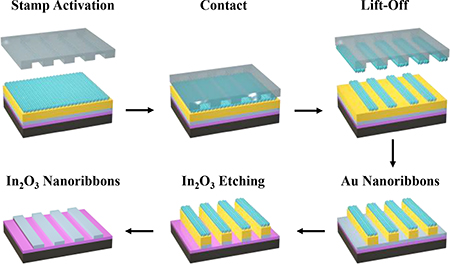
One-dimensional (1D) nanomaterials, such as nanowires, nanotubes, and nanoribbons, possess large surface-to-volume ratios and tunable physical properties. These characteristics can be leveraged to achieve superior performance over bulk materials in a variety of applications, including electronics,1–5 optics and photonics,6–10 energy-storage and conversion devices,11,12 biological and chemical sensors,13–19 intracellular delivery of bioactive molecules,20 and medical devices.21,22 For example, Si nanowires (SiNWs) and carbon nanotubes (CNTs) have been employed as channel components in field-effect transistors (FETs) for highly effective sensing of proteins,23,24 DNA,25,26 viruses,27 and neurotransmitters.28 However, significant problems remain to be solved before 1D nanomaterials find widespread use.
Bottom-up techniques, such as chemical vapor deposition (CVD) and solution processes,29–33 dominate 1D-nanomaterial fabrication. However, these strategies have poor control over the orientations of as-grown nanostructures, often on substrates other than the final devices. Bottom-up methods require additional steps to transfer nanostructures and then to control their positions and orientations in devices.34,35 For example, SiNWs and CNTs, typically synthesized by CVD, require precise control over specific growth parameters to produce high-quality 1D nanomaterials suitable for electronic devices.29,36 Moreover, nanowires synthesized by CVD are randomly orientated greatly increasing the complexity of device fabrication.37 Performance is limited by poor control over the numbers of functional nanowires present in devices.38,39
Top-down approaches, including photolithography and electron-beam lithography (EBL), are widely used in the semiconductor industry to fabricate 1D nanomaterials. Top-down methods enable precise control over final shapes, sizes, positions, and orientations of the as-fabricated structures,40,41 providing ready integration with devices and high reproducibility.42,43 Nonetheless, top-down techniques suffer from substantial equipment and usage costs. Patterns produced via photolithography are limited by the resolution of the optical imaging system, often to micron-scale features. By contrast, EBL achieves nanometer-resolution patterning but at the expense of time-consuming serial writing processes. These drawbacks represent significant barriers for many users, hence the need for alternative high-throughput, economical nanoscale patterning strategies.
Recently, we reported a straightforward, high-fidelity nanopatterning technique called chemical lift-off lithography (CLL),44–48 wherein oxygen plasma-activated polydimethylsiloxane (PDMS) stamps selectively remove portions of a self-assembled monolayer (SAM) in contacted areas without observable lateral diffusion at feature edges. The remaining SAM molecules in the non-contacted regions act as molecular resists during subsequent etching of the freshly exposed underlying substrate. We previously demonstrated that CLL can be used to simplify device fabrication, as well as to enable biomolecule patterning to investigate DNA hybridization and spin-selective electron transport.49–53 High-fidelity chemical patterns with line widths as narrow as 40 ± 2 nm were achieved using CLL, with the possibility of features as narrow as 5 nm (corresponding to ~10 molecules).46 As with other top-down patterning approaches, however, CLL relies on expensive nanofabricated masters to create PDMS stamps to produce nanoscale structures. Masters for CLL have been produced using low-throughput EBL methods, limiting impact.47,48
Many top-down nanofabrication processes, including CLL, have focused on patterning metals and group IV and III-V semiconductors (e.g., Au and Si).54 Metal oxides represent an increasingly important material class in numerous applications due to their electronic, mechanical, and optical properties.45,55–57 To date, top-down approaches for fabricating metal-oxide nanomaterials are under developed compared to patterning methods for other types of materials, yet patterned semiconductors are of interest for applications including electronics, displays and lighting, ultra-sensitive biosensors, and wearable, flexible sensors.58–60
We report on the fabrication of large-area In2O3 nanoribbon arrays using CLL, but without using masters generated via EBL. We utilize metal oxide nanoribbons as semiconducting channels in FET architectures. Through this demonstration, we extend the range and applicability of CLL patterning to nanoscale features on semiconducting, metal oxides for functional electronic devices, achieving current on/off ratios of ~107 and a peak mobility of 13.7 cm2 V−1 s−1, in a low-cost, high-throughput manner.
Most commonly used thin-film metal oxide deposition strategies rely on physical/chemical vapor deposition methods, such as pulsed-laser deposition,61 sputtering,62 and atomic-layer deposition,63 requiring complex processes, extreme conditions (e.g., high temperature, vacuum), and costly equipment. Recently, simple, scalable sol-gel-based processes have emerged as alternatives for preparing high quality semiconducting metal-oxide films.64–67 Here, thin films of In2O3 were prepared via a sol-gel process. Aqueous solutions (0.1 M) of In(NO3)3 were spin-coated onto SiO2/Si substrates (100 nm, thermally grown SiO2 dielectric on heavily doped, p-type Si substrates with resistivities of 1–5 mΩ·cm). Following deposition, substrates were heated to 100 °C for 5 min and annealed at 250 °C for 3 h. The thicknesses of the resulting In2O3 films were ~3 nm with typical surface roughnesses of ~0.06 nm determined via atomic force microscopy (AFM) (Figure S1).
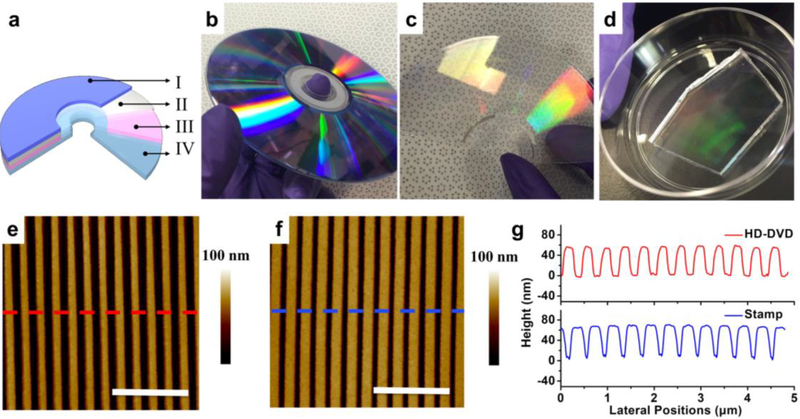
Commercially available optical storage media, such as compact discs (CDs) and DVDs are patterned with sub-micron periodic gratings that can be used directly as economical templates for soft lithography. We employed HD-DVDs as masters for CLL PDMS stamps. The HD-DVDs have quasi-1D feature widths of ~200 nm, spaced at a pitch of 400 nm. As shown in Figure 1a, each HD-DVD is composed of a protection layer (I), a reflective layer (II), a recording layer (III), and a polycarbonate layer (IV) composed of embossed concentric rings that form the basis of the patterns used herein. Layer IV was exposed simply by removing layers I and II with a razor blade and dissolving layer III with ethanol (Figure 1c). Atomic force microscopy (AFM) confirmed the expected, grooved pattern on the surface of layer IV, as seen in Figure 1e. To replicate layer IV features precisely, hard PDMS (h-PDMS) was used as the stamp material due to its stiffness compared to regular (soft) Sylgard 184 PDMS.68 Unpolymerized h-PDMS was spin-coated onto masters (2 cm × 2 cm, 40 s at 1000 rpm) and cured at 65 °C for 10 min to form thin and robust films. A layer of soft PDMS (~5 mm) was then applied and cured at 65 °C overnight to form a support for the pattern-containing h-PDMS film and to prevent cracking, prior to demolding stamps from masters. These stamps (Figure 1d) are reusable and can be employed for repeated, wafer-scale CLL patterning. Atomic-force micrographs of patterned PDMS surfaces (Figure 1f) confirmed precise replication of HD-DVD features with depths of ~60 nm.
Figure 1.
(a) Schematic architecture of a high-definition digital-versatile disc (HD-DVD): Layer I, polycarbonate protective layer; Layer II, mirror-like metal film; Layer III, data recording film; Layer IV, polycarbonate layer containing concentric rings with typical widths of 250 nm and periodicities of 400 nm. (b-d) Photographs of an HD-DVD, an HD-DVD master (Layer IV), and a patterned polydimethylsiloxane (PDMS) stamp, respectively. Atomic force micrographs of a representative HD-DVD master (e) and a patterned PDMS stamp (f). Scale bars are 2 εm. (g) Topographic profiles across the corrugated features in (e) and (f).
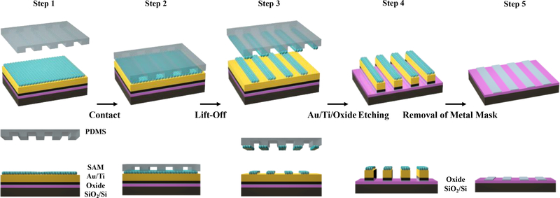
The scheme used to fabricate In2O3 nanoribbons is illustrated in Figure 2. Step 1: layers of Ti (10 nm) and Au (30 nm) were deposited on previously prepared In2O3 films. The Au/Ti/In2O3/SiO2/Si stacks were then incubated in 1 mM ethanolic solutions of 11-mercapto-1-undecanol (HSCH2(CH2)9CH2OH) to form SAMs terminated with –OH moieties, enabling CLL patterning. Step 2: an oxygen plasma was used to “activate” PDMS stamp surfaces, generating siloxyl groups (SiOH). Stamps were then brought into conformal contact with SAMs. Condensation reactions occur between the hydroxyl- (–OH) terminated SAMs and the SiOH groups of the activated h-PDMS, forming covalent linkages (Si–O–SAM). Step 3: Upon removal of the stamps, molecules within the contracted regions of the SAMs were selectively removed transferring the stamp pattern to the monolayer. Notably, in the lift-off process, monolayers of Au atoms are also removed as Au–S bonds (between SAM molecules and the underlying Au substrate atoms) are stronger than Au–Au bonds in the substrates.
Figure 2.
Fabrication scheme of In2O3 nanoribbons. Step 1: a thin film of 3-nm In2O3 was deposited on a SiO2/Si substrate via a sol-gel process followed by Au (30 nm)/Ti (10 nm) deposition and functionalization with a self-assembled monolayer (SAM). Step 2: a polydimethylsiloxane (PDMS) stamp, activated by an oxygen plasma, was brought into conformal contact with the substrate. Step 3: Upon lifting the stamp from the surface, SAM molecules in the contacted areas were removed, transferring the pattern (periodic lines and spaces) into the SAM. Step 4: Successive selective etch processes removed Au/Ti and In2O3 layers from unprotected regions on the surface. Step 5: Remaining SAM, Au, and Ti were removed to produce In2O3 nanoribbon arrays.
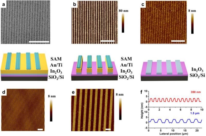
Scanning electron microscopy of CLL-patterned SAMs (Figure 3a) confirmed the presence of 1D features (200 nm linewidths) over large areas, matching those on the stamps (Figure 1f). Step 4: Intact monolayers in the non-contacted regions acted as resists for successive etching by solutions of Fe(NO3)3 and thiourea (removing exposed Au) and EDTA disodium salt, NH4OH, and H2O2 (removing Ti), thereby transferring the SAM patterns through the metal layers. The metal layers acted as etch masks protecting the underlying In2O3 films from removal by glacial acetic acid. The resulting Au/Ti/In2O3 nanoribbons were investigated by AFM (Figure 3b) and found to have heights of ~45 nm, corresponding to the sum of the expected heights of the constituent layers above the surrounding Si/SiO2 surfaces exposed by previous etch processes. Step 5: metal layers were completely removed to expose arrays of In2O3 nanoribbons extending over centimeter length scales (Figure 3c). The widths (~200 nm) and heights (~3 nm) of the metal oxide nanoribbons are the smallest, to our knowledge, fabricated via top-down approaches.
Figure 3.
(a) Scanning electron microscope image (top) and schematic (bottom) of a self-assemble monolayer (SAM) patterned via chemical lift-off lithography. (b, c) Topographic images measured using atomic force microscopy (AFM), top, and schematic illustrations, bottom, of SAM/Au/Ti/In2O3 and bare In2O3 nanoribbons, respectively, with line widths of ~200 nm. Atomic force topographs of In2O3 nanoribbons with line widths of (d) 350 nm and (e) 1.5 εm. Thicknesses of each set of In2O3 nanoribbons (c-e) were measured to be ~3 nm by AFM. (f) Height profiles of 500 nm wide In2O3 nanoribbons (top) and 1.5 εm wide nanoribbons (bottom). Scale bars in all images represent distances of 3 εm.
To demonstrate the versatility of CLL patterning for additional feature sizes, In2O3 nanoribbons of different linewidths (350 nm and 1500 nm) were fabricated using alternate master patterns (Figure 3d and 3e, respectively). The Au nanoribbons produced as an intermediate product of this process (Step 4) can also be used for a variety of applications, such as surface plasmon resonance biosensors. We note that In2O3 nanoribbon edges are rougher than those of similarly produced Au nanoribbons; this is a common phenomenon associated with isotropic etch processes, which can undercut regions below the protective masks.
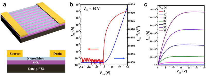
Field-effect transistors have key advantages over optical or electrochemical platforms for biosensing applications, including low detection limits, real-time and label-free measurements, and simple integration with standard semiconductor-device processing.45 To evaluate the performance of In2O3 nanoribbons in devices, we constructed FETs in a bottom-gate, top-contact configuration as shown in Figure 4. Gold electrodes were deposited atop arrays of as-prepared In2O3 nanoribbons via electron-beam evaporation through a shadow mask. As shown in Figure S3, interdigitated electrodes with widths of 1300 εm and lengths of 45 εm were used.
Figure 4.
(a) Schematic illustrations of an In2O3 field-effect transistor (FET) in a bottom-gate-top-contact configuration. Gate: Si (p++); Source/Drain: Au; semiconducting channel: In2O3 nanoribbons. The widths and lengths of the inter-digital electrodes are 1300 and 45 εm, respectively. The widths and pitches of the nanoribbons are 200 and 400 nm, respectively. (b) Transfer and (c) output characteristics of an ultrathin In2O3 nanoribbon FET, showing the measured current between the drain and source (IDS) in response to varying gate to source voltages (VGS) and source to drain (VDS) potentials, relative to the source. Devices displayed n-type pinch-off behavior with carrier motilities of 10.0 ± 2.6 cm2 V−1 s−1, averaged over 10 devices with a peak value of 13.7 cm2 V−1 s−1, and a current on/off ratio >107.
The spatially ordered arrangement of In2O3 nanoribbons on surfaces facilitated straightforward fabrication of FETs with consistent numbers of channels per device, controlled by the widths of the contact electrodes. Here, ~3000 200-nm-wide In2O3 nanoribbons were incorporated into each FET device. These FETs had high field-effect mobilities (μsat=10.0 ± 2.6 cm2 V−1 s−1), averaged over 10 devices with a peak value of 13.7 cm2 V−1 s−1 and a current on/off ratio >107. The performance of these devices exceeded those previously reported for 1D nanowire-based devices fabricated via bottom-up approaches. High-performance In2O3 nanoribbon FETs can be used in a variety of applications, such as ultrasensitive FET-based chemical, and biological sensors.
In summary, we report a high-throughput, large-scale strategy enabling fabrication of ultrathin, metal oxide nanoribbons that are readily integrated into devices. We leverage and extend the capabilities of CLL, in combination with selective etching processes, to pattern, successively, SAMs, metal films, and ultra-thin layers of In2O3 to create arrays of periodic, 1D nanostructures. Nanoribbons fabricated by this approach are uniform and continuous over centimeter scales. We demonstrate high performance FETs fabricated using In2O3 nanoribbons having carrier mobilities up to 13.7 cm2 V−1 s−1 and on/off current ratios >107, making these nanoribbons promising materials for electronic devices, large-area displays, and sensors. By employing widely available low-cost HD-DVDs as nanostructured master patterns, in conjunction with CLL, a scalable and high-fidelity chemical patterning technique that does not require sophisticated equipment and facilities, we lower barriers to nanostructure fabrication. The advances demonstrated here serve to extend large-area nanofabrication and to broadened application and user bases by providing alternative patterning strategies to photo- and electron-beam lithographies.
Supplementary Material
ACKNOWLEDGMENTS
This work was supported by National Science Foundation (CMMI-1636136) and the National Institute on Drug Abuse (DA045550). We acknowledge the facilities and thank the staff of the Nanoelectronics Research Facility (NRF), Electron Imaging Center, Nano & Pico Characterization Lab, and Integrated Systems Nanofabrication Cleanroom of the California NanoSystems Institute. The authors thank Dr. Jeffrey J. Schwartz for assistance in writing the manuscript.
Footnotes
Supporting Information.
Experimental details; Figure S1-S3; Fabrication process of HD DVD masters, DVD-masters, Si masters and h-PDMS stamps; Characterization of chemical patterns and stamps; Surface functionalization; Activation of PDMS stamps; Au, Ti, and In2O3 selective wet-etching processes; Surface roughness characterization of the In2O3; Photographs of fabricated devices and FETs measurements; Photograph of interdigitated electrodes.
REFERENCES
- (1).Cui Y; Lieber CM Science 2001, 291, 851–853. [DOI] [PubMed] [Google Scholar]
- (2).Xu X; Liu C; Kim K; Fan DL Adv. Funct. Mater. 2014, 24, 4843–4850. [Google Scholar]
- (3).Memisevic E; Hellenbrand M; Lind E; Persson AR; Sant S; Schenk A; Svensson J; Wallenberg R; Wernersson LE Nano Lett. 2017, 17, 4373–4380. [DOI] [PubMed] [Google Scholar]
- (4).Lee H; Manorotkul W; Lee J; Kwon J; Suh YD; Paeng D; Grigoropoulos CP; Han S; Hong S; Yeo J; Ko SH ACS Nano 2017, 11, 12311–12317. [DOI] [PubMed] [Google Scholar]
- (5).Qiu C; Zhang Z; Xiao M; Yang Y; Zhong D; Peng LM Science 2017, 355, 271–276. [DOI] [PubMed] [Google Scholar]
- (6).Huang MH; Mao S; Feick H; Yan H; Wu Y; Kind H; Weber E; Russo R; Yang P Science 2001, 292, 1897–1899. [DOI] [PubMed] [Google Scholar]
- (7).Law M; Sirbuly DJ; Johnson JC; Goldberger J; Saykally RJ; Yang P Science 2004, 305, 1269–1273. [DOI] [PubMed] [Google Scholar]
- (8).Xu X; Kim K; Fan D Angew. Chem., Int. Ed. 2015, 54, 2525–2529. [DOI] [PMC free article] [PubMed] [Google Scholar]
- (9).Liu P; He X; Ren J; Liao Q; Yao J; Fu H ACS Nano 2017, 11, 5766–5773. [DOI] [PubMed] [Google Scholar]
- (10).Xu X; Yang Q; Wattanatorn N; Zhao C; Chiang N; Jonas SJ; Weiss PS ACS Nano 2017, 11, 10384–10391. [DOI] [PubMed] [Google Scholar]
- (11).Law M; Greene LE; Johnson JC; Saykally R; Yang P Nat. Mater. 2005, 4, 455–459. [DOI] [PubMed] [Google Scholar]
- (12).Zhang L; Jia Y; Wang S; Li Z; Ji C; Wei J; Zhu H; Wang K; Wu D; Shi E; Fang Y; Cao A Nano Lett. 2010, 10, 3583–3589. [DOI] [PubMed] [Google Scholar]
- (13).Kong J Science 2000, 287, 622–625. [DOI] [PubMed] [Google Scholar]
- (14).Cui Y; Wei Q; Park H; Lieber CM Science 2001, 293, 1289–1292. [DOI] [PubMed] [Google Scholar]
- (15).Li C; Zhang D; Liu X; Han S; Tang T; Han J; Zhou C Appl. Phys. Lett. 2003, 82, 1613–1615. [Google Scholar]
- (16).Zhang D; Liu Z; Li C; Tang T; Liu X; Han S; Lei B; Zhou C Nano Lett. 2004, 4, 1919–1924. [Google Scholar]
- (17).Cheng Y; Xiong P; Yun CS; Strouse GF; Zheng JP; Yang RS; Wang ZL Nano Lett. 2008, 8, 4179–4184. [DOI] [PMC free article] [PubMed] [Google Scholar]
- (18).Xu X; Li H; Hasan D; Ruoff RS; Wang AX; Fan DL Adv. Funct. Mater. 2013, 23, 4332–4338. [Google Scholar]
- (19).Kim K; Xu X; Guo J; Fan DL Nat. Commun. 2014, 5, 3632. [DOI] [PubMed] [Google Scholar]
- (20).Xu X; Hou S; Wattanatorn N; Wang F; Yang Q; Zhao C; Yu X; Tseng H-R; Jonas SJ; Weiss PS ACS Nano 2018, Article ASAP, DOI: 10.1021/acsnano.1028b00763. [DOI] [PubMed] [Google Scholar]
- (21).Kim J; Lee M; Shim HJ; Ghaffari R; Cho HR; Son D; Jung YH; Soh M; Choi C; Jung S; Chu K; Jeon D; Lee ST; Kim JH; Choi SH; Hyeon T; Kim DH Nat. Commun 2014, 5, 5747. [DOI] [PubMed] [Google Scholar]
- (22).Liu R; Chen R; Elthakeb AT; Lee SH; Hinckley S; Khraiche ML; Scott J; Pre D; Hwang Y; Tanaka A; Ro YG; Matsushita AK; Dai X; Soci C; Biesmans S; James A; Nogan J; Jungjohann KL; Pete DV; Webb DB; Zou Y; Bang AG; Dayeh SA Nano Lett. 2017, 17, 2757–2764. [DOI] [PMC free article] [PubMed] [Google Scholar]
- (23).So HM; Won K; Kim YH; Kim BK; Ryu BH; Na PS; Kim H; Lee JO J. Am. Chem. Soc. 2005, 127, 11906–11907. [DOI] [PubMed] [Google Scholar]
- (24).Stern E; Vacic A; Rajan NK; Criscione JM; Park J; Ilic BR; Mooney DJ; Reed MA; Fahmy TM Nat. Nanotechnol. 2010, 5, 138–142. [DOI] [PMC free article] [PubMed] [Google Scholar]
- (25).Hahm J. -i.; Lieber CM Nano Lett. 2004, 4, 51–54. [Google Scholar]
- (26).Sorgenfrei S; Chiu CY; Gonzalez RL Jr.; Yu YJ; Kim P; Nuckolls C; Shepard KL Nat. Nanotechnol. 2011, 6, 126–132. [DOI] [PMC free article] [PubMed] [Google Scholar]
- (27).Patolsky F; Zheng G; Hayden O; Lakadamyali M; Zhuang X; Lieber CM Proc. Natl. Acad. Sci. U. S. A. 2004, 101, 14017–14022. [DOI] [PMC free article] [PubMed] [Google Scholar]
- (28).Li BR; Hsieh YJ; Chen YX; Chung YT; Pan CY; Chen YT J. Am. Chem. Soc. 2013, 135, 16034–16037. [DOI] [PubMed] [Google Scholar]
- (29).Patolsky F; Zheng G; Lieber CM Nat. Protoc. 2006, 1, 1711–1724. [DOI] [PubMed] [Google Scholar]
- (30).Wang ZL Science 2006, 312, 242–246. [DOI] [PubMed] [Google Scholar]
- (31).Liu C; Xu X; Rettie AJE; Mullins CB; Fan DL J. Mater. Chem. A 2013, 1, 8111. [Google Scholar]
- (32).Gao N; Zhou W; Jiang X; Hong G; Fu TM; Lieber CM Nano Lett. 2015, 15, 2143–2148. [DOI] [PMC free article] [PubMed] [Google Scholar]
- (33).Constantinou M; Rigas GP; Castro FA; Stolojan V; Hoettges KF; Hughes MP; Adkins E; Korgel BA; Shkunov M ACS Nano 2016, 10, 4384–4394. [DOI] [PubMed] [Google Scholar]
- (34).Xu F; Durham JW; Wiley BJ; Zhu Y ACS Nano 2011, 5, 1556–1563. [DOI] [PubMed] [Google Scholar]
- (35).Yao J; Yan H; Lieber CM Nat. Nanotechnol. 2013, 8, 329–335. [DOI] [PubMed] [Google Scholar]
- (36).Alam SB; Panciera F; Hansen O; Molhave K; Ross FM Nano Lett. 2015, 15, 6535–6541. [DOI] [PubMed] [Google Scholar]
- (37).Ishikawa FN; Curreli M; Chang HK; Chen PC; Zhang R; Cote RJ; Thompson ME; Zhou C ACS Nano 2009, 3, 3969–3976. [DOI] [PMC free article] [PubMed] [Google Scholar]
- (38).Li J; Zhang Y; To S; You L; Sun Y ACS Nano 2011, 5, 6661–6668. [DOI] [PubMed] [Google Scholar]
- (39).Lee BY; Sung MG; Lee J; Baik KY; Kwon YK; Lee MS; Hong S ACS Nano 2011, 5, 4373–4379. [DOI] [PubMed] [Google Scholar]
- (40).Stern E; Klemic JF; Routenberg DA; Wyrembak PN; Turner-Evans DB; Hamilton AD; LaVan DA; Fahmy TM; Reed MA Nature 2007, 445, 519–522. [DOI] [PubMed] [Google Scholar]
- (41).Knopfmacher O; Tarasov A; Fu W; Wipf M; Niesen B; Calame M; Schonenberger C Nano Lett. 2010, 10, 2268–2274. [DOI] [PubMed] [Google Scholar]
- (42).Tong HD; Chen S; van der Wiel WG; Carlen ET; van den Berg A Nano Lett. 2009, 9, 1015–1022. [DOI] [PubMed] [Google Scholar]
- (43).Hwang SW; Lee CH; Cheng H; Jeong JW; Kang SK; Kim JH; Shin J; Yang J; Liu Z; Ameer GA; Huang Y; Rogers JA Nano Lett. 2015, 15, 2801–2808. [DOI] [PubMed] [Google Scholar]
- (44).Liao WS; Cheunkar S; Cao HH; Bednar HR; Weiss PS; Andrews AM Science 2012, 337, 1517–1521. [DOI] [PubMed] [Google Scholar]
- (45).Kim J; Rim YS; Chen H; Cao HH; Nakatsuka N; Hinton HL; Zhao C; Andrews AM; Yang Y; Weiss PS ACS Nano 2015, 9, 4572–4582. [DOI] [PubMed] [Google Scholar]
- (46).Andrews AM; Liao WS; Weiss PS Acc. Chem. Res. 2016, 49, 1449–1457. [DOI] [PubMed] [Google Scholar]
- (47).Xu X; Yang Q; Cheung KM; Zhao C; Wattanatorn N; Belling JN; Abendroth JM; Slaughter LS; Mirkin CA; Andrews AM; Weiss PS Nano Lett. 2017, 17, 3302–3311. [DOI] [PubMed] [Google Scholar]
- (48).Zhao C; Xu X; Yang Q; Man T; Jonas SJ; Schwartz JJ; Andrews AM; Weiss PS Nano Lett. 2017, 17, 5035–5042. [DOI] [PubMed] [Google Scholar]
- (49).Cao HH; Nakatsuka N; Serino AC; Liao WS; Cheunkar S; Yang H; Weiss PS; Andrews AM ACS Nano 2015, 9, 11439–11454. [DOI] [PubMed] [Google Scholar]
- (50).Abendroth JM; Nakatsuka N; Ye M; Kim D; Fullerton EE; Andrews AM; Weiss PS ACS Nano 2017, 11, 7516–7526. [DOI] [PubMed] [Google Scholar]
- (51).Cao HH; Nakatsuka N; Liao W-S; Serino AC; Cheunkar S; Yang H; Weiss PS; Andrews AM Chem. Mater. 2017, 29, 6829–6839. [Google Scholar]
- (52).Chen CY; Wang CM; Chen PS; Liao WS Chem. Comm 2018. [Google Scholar]
- (53).Chen CY; Wang CM; Chen PS; Liao WS Nanoscale 2018, 10, 3191–3197. [DOI] [PubMed] [Google Scholar]
- (54).Ko H; Takei K; Kapadia R; Chuang S; Fang H; Leu PW; Ganapathi K; Plis E; Kim HS; Chen SY; Madsen M; Ford AC; Chueh YL; Krishna S; Salahuddin S; Javey A Nature 2010, 468, 286–289. [DOI] [PubMed] [Google Scholar]
- (55).Rim YS; Bae SH; Chen H; Yang JL; Kim J; Andrews AM; Weiss PS; Yang Y; Tseng HR ACS Nano 2015, 9, 12174–12181. [DOI] [PubMed] [Google Scholar]
- (56).Chen H; Rim YS; Wang IC; Li C; Zhu B; Sun M; Goorsky MS; He X; Yang Y ACS Nano 2017, 11, 4710–4718. [DOI] [PubMed] [Google Scholar]
- (57).Rim YS; Chen H; Zhu B; Bae S-H; Zhu S; Li PJ; Wang IC; Yang Y Adv. Mater. Inter. 2017, 4, 1700020. [Google Scholar]
- (58).Aroonyadet N; Wang X; Song Y; Chen H; Cote RJ; Thompson ME; Datar RH; Zhou C Nano Lett. 2015, 15, 1943–1951. [DOI] [PubMed] [Google Scholar]
- (59).Liu Q; Aroonyadet N; Song Y; Wang X; Cao X; Liu Y; Cong S; Wu F; Thompson ME; Zhou C ACS Nano 2016, 10, 10117–10125. [DOI] [PubMed] [Google Scholar]
- (60).Liu Q; Liu Y; Wu F; Cao X; Li Z; Alharbi M; Abbas AN; Amer MR; Zhou C ACS Nano 2018, 12, 1170–1178. [DOI] [PubMed] [Google Scholar]
- (61).Nomura K; Ohta H; Takagi A; Kamiya T; Hirano M; Hosono H Nature 2004, 432, 488–492. [DOI] [PubMed] [Google Scholar]
- (62).Martins RFP; Ahnood A; Correia N; Pereira LMNP; Barros R; Barquinha PMCB; Costa R; Ferreira IMM; Nathan A; Fortunato EE M. C. Adv. Funct. Mater. 2013, 23, 2153–2161. [Google Scholar]
- (63).Lin YY; Hsu CC; Tseng MH; Shyue JJ; Tsai FY ACS Appl. Mater. Inter. 2015, 7, 22610–22617. [DOI] [PubMed] [Google Scholar]
- (64).Kim HS; Byrne PD; Facchetti A; Marks TJ J. Am. Chem. Soc. 2008, 130, 12580–12581. [DOI] [PubMed] [Google Scholar]
- (65).Banger KK; Yamashita Y; Mori K; Peterson RL; Leedham T; Rickard J; Sirringhaus H Nat. Mater 2011, 10, 45–50. [DOI] [PubMed] [Google Scholar]
- (66).Hwan Hwang Y; Seo J-S; Moon Yun J; Park H; Yang S; Ko Park S-H; Bae B-S NPG Asia Mater. 2013, 5, e45. [Google Scholar]
- (67).Rim YS; Chen H; Song T-B; Bae S-H; Yang Y Chem. Mater 2015, 27, 5808–5812. [Google Scholar]
- (68).Qin D; Xia Y; Whitesides GM Nat. Protoc. 2010, 5, 491–502. [DOI] [PubMed] [Google Scholar]
Associated Data
This section collects any data citations, data availability statements, or supplementary materials included in this article.


