Abstract
Tin doped indium oxide (ITO) thin films provide excellent transparency and conductivity for electrodes in displays and photovoltaic systems. Current advances in producing printable ITO inks are reducing the volume of wasted indium during thin film patterning. However, their applicability to flexible electronics is hindered by the need for high temperature processing that results in damage to conventional polymer substrates. Here, we detail the conditions under which laser heating can be used as a replacement for oven and furnace treatments. Measurements of the optical properties of both the printed ITO film and the polymer substrate (polyethylene terephthalate, PET) identify that in the 1.5–2.0 μm wavelength band there is absorption in the ITO film but good transparency in PET. Hence, laser light that is not absorbed in the film does not go on to add a deleterious energy loading to the substrate. Localization of the energy deposition in the film is further enhanced by using ultrashort laser pulses (~1 ps) thus limiting heat flow during the interaction. Under these conditions, laser processing of the printed ITO films results in an improvement of the conductivity without damage to the PET.
Introduction
Transparent conductive oxide (TCO) films are widely used in a variety of optoelectronic devices, such as solar cells1,2, liquid crystal displays (LCD)3, touch screens4,5, and light-emitting diodes (LED)6–8. One of the most popular materials is indium tin oxide (ITO), mainly due to its high transparency in the visible part of the spectrum and relatively low resistivity (in the region 1 − 2 × 10⁻⁴ )9. ITO films can be deposited via chemical vapour deposition10, spray pyrolysis11, and evaporation12 but the most commonly used technique is magnetron sputtering13,14. All of these techniques require either a high substrate temperature during deposition (300–500 °C) or a high-temperature (400–700 °C) annealing treatment to meet the transparency and resistivity criteria of most applications. Consequently, the use of polymer substrates is limited in scope as their upper working temperature would be exceeded. Further patterning steps may also compromise the substrate integrity.
Solution-based deposition methods, such as inkjet15 and gravure printing16–19 are considered to be one of the possible ways to increase material utilization (as lossy post patterning is not required), reduce costs and improve compatibility with the heat-sensitive (e.g. polymer) substrates20. Generally, the films produced via these techniques consist of conducting nanoparticles capped with organic stabilizers. Such stabilizers between the particles lead to fewer percolation paths in the films and, in turn, higher resistivity values. This problem is typically addressed by a so-called sintering process, during which conductive neck formation between the particles, accompanied by the removal of stabilizers, occurs. Such thermal sintering has been shown to result in transparency values comparable to that of sputtered films; the resistivity values, however, remained one to two orders of magnitude higher21–23. Moreover, such an approach requires high-temperatures (400–600 °C), consequently making it ineffective for heat-sensitive substrates. Apart from conventional heating, there are several low-temperature sintering techniques, including chemical sintering24, compression25, electrophoretic deposition26, hydrothermal crystallization27, microwave irradiation28, plasma treatment29, and photonic sintering30–32. The last of these examples32 includes laser and intense pulsed light (IPL) sintering33, and is of particular interest due to its simplicity34, relatively low cost and high throughput35,36. The main drawback of the IPL method is that due to the high absorbance of most polymers in the infrared region of spectrum it becomes difficult to implement for flexible substrates37. The laser sintering approach heavily relies on the optical properties of nanoparticles in the film; one has to choose the radiation source according to their absorption spectrum. This can be easily achieved for the most commonly used metal nanoparticles (Au38, Ag39, Cu31), whose plasmon resonance peaks are located in the visible part of the spectrum40, however sintering of TCO particles becomes a challenging task due to their high transparency in that spectral region. Nevertheless, it has been shown that effective sintering of such nanoparticles is feasible using UV excimer lasers by specifically adding compounds to the ink with high absorption at the incident beam wavelength41–43. More recently it has been shown that effective excimer laser annealing of a film consisting solely of ITO nanoparticles is possible44. The sheet resistance of the film, however, remained relatively high (500 /sq) and the exact optical transmission values were not reported. Another possible approach to laser sintering of TCO films is to utilize near-infrared radiation sources (0.75–3 μm). In the spectral region of 1.5–3 μm the absorption of TCO particles is dominated by the presence of free electrons and reaches its maximum values8. At the same time, typical polymer substrates remain highly transparent up to about 2 μm36,37. Several types of radiation sources are currently available in this spectral region, including erbium doped glass (wavelength of 1.54 μm), Ho:YAG (2.01 μm), and Tm:YAG (2.04 μm) lasers45. One can also obtain a laser source with a near IR spectrum by adding a set of filtering optics to one with a wider emission spectrum (e.g. a supercontinuum fibre laser46). Despite this, there are very few reports of near-infrared laser sintering of TCO films. One study47 investigated the interaction of a CW Erbium fiber laser radiation with ITO films on a high temperature substrate. They showed that such treatment results in a film resistivity decrease to about 1.3 × 10⁻³ 47. However, as a CW laser was used, it remains unclear whether this method can be applied to polymer substrates with lower working temperatures. This paper investigates the effects of supercontinuum picosecond laser irradiation of ITO films gravure-printed on flexible (PET) foils. The ITO ink consisted of ITO nanoparticles dispersed in a solvent with an addition of a binder16–18. The choice of laser allowed selection of the most appropriate wavelength band as informed by the optical measurements. The emission spectrum of the laser was filtered to achieve maximum absorption of the laser light in the ITO particles whilst leaving the substrate undamaged and limiting heat flow due to its picosecond pulse duration. It is shown that such treatment leads to effective sintering of the particles, significantly improving the electronic properties of the film.
Results and Discussion
Optical Coupling
The optical absorption coefficients for the ITO film and PET substrate were measured in the wavelength range 250 nm to 2000 nm (Fig. 1). It can be seen that in the visible wavelength region, there is excellent transparency for the PET and, although the unirradiated ITO layer has an absorption coefficient of 3 × 104 cm−1, this corresponds to an absorption depth of 2.5 μm which is far in excess of the thickness. For ultraviolet wavelengths, both the film and substrate exhibit strong absorption and any light that does penetrate the ITO will be then absorbed in the PET. This adds an energy loading to the substrate that is to be avoided so as to not compromise its mechanical and optical properties. Whereas, in the near IR, strong absorption is seen in the ink layer whilst the PET remains transparent (Fig. 1). It is for this reason that we have explored laser irradiation using near IR wavelengths and also exploited short pulse durations. The optical energy was supplied by a filtered white light laser (see Experimental section) as shown in Fig. 2. Approximately 97% of the laser energy is absorbed in the film (integrated over the emission spectrum of the laser). Taking 1750 nm as the centre of the filtered laser spectrum, the absorption coefficient of the ITO is 105 cm−1 resulting in 5% of the energy reaching the substrate. This energy is then distributed over the entire thickness of PET as the absorption depth (~1 mm) exceeds the substrate thickness of 250 μm.
Figure 1.
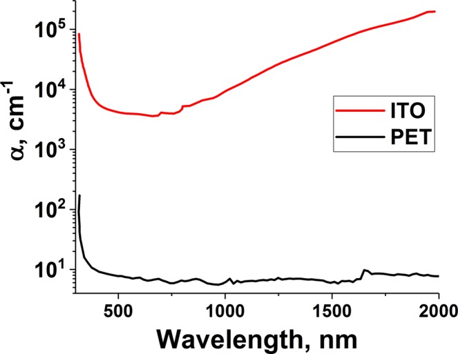
Optical absorption spectra for as-deposited ITO (before laser irradiation) and the PET substrate. The ITO increases in absorption in the near infra red whereas the PET remains transparent.
Figure 2.
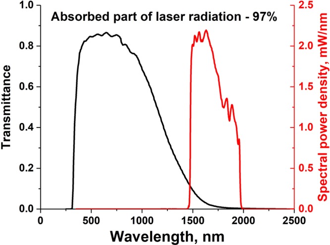
Normalized transmission spectrum of the unirradiated ITO film (black curve) and the emission spectrum of the filtered white light laser radiation (red curve).
Conductivity and Transparency
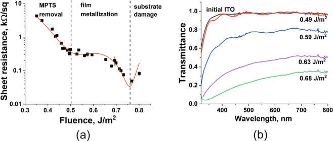
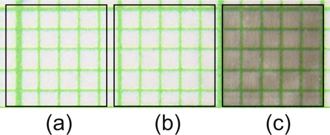
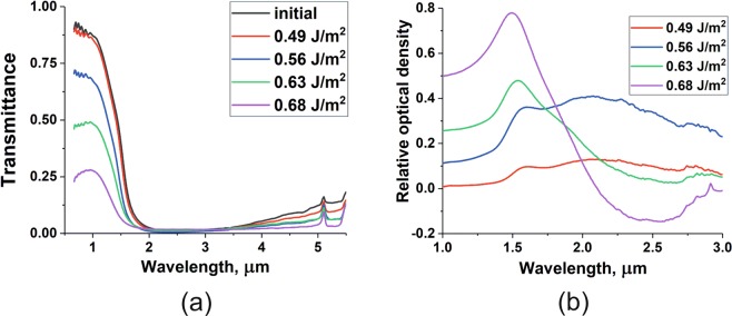
The main objective of laser sintering of wet-processed ITO films is to increase their conductivity whilst retaining transparency in the visible spectrum. A series of laser exposures were carried out to investigate the dependence of film sheet resistance on irradiation parameters. The results of such studies are given in Fig. 3(a). It can be seen in Fig. 3(a) that the sheet resistance of the films depends non-monotonously on laser fluence. The line is included to guide the eye and shows that after an initial decrease in resistance of approximately one order of magnitude, the effect is seen to saturate. One can ascribe this phenomenon to removal of the binder (MPTS) causing change in average distance between the ITO nanoparticles, which is known to significantly affect the conductivity of the film48. The observed saturation corresponds to the point where no binder is left in the film composition. Increasing the fluence beyond ~0.7 Jm−2 causes the resistance to begin to decrease again until damage is observed above 0.75 Jm−2 with a concomitant loss of material and conductivity. For most applications, such as electrical contacts for displays or photovoltaic cells, a high level of transparency is required. Figure 3(b) shows that the optical transmission spectra exhibit a very low degree of oscillation in the blue region, indicating good refractive index matching to the substrate. However, the transmission of the film-substrate system becomes compromised as the incident fluence is increased. The irradiation conditions correspond to the plateau region seen in Fig. 3(a). We interpret this behaviour as the film becoming more metallic in character, caused by the laser-induced sintering of ITO nanoparticles. Consequently, its conductivity improves but its opacity increases, as qualitatively shown in Fig. 4. This is often more easily identified in the near infra red as the so-called plasma edge is seen to move to higher frequencies. Therefore, near IR spectra were measured (Fig. 5(a)). It can be seen that there is a subtle shift in the cut-off around 1.5 μm towards shorter wavelengths (higher frequencies). To explore further, this data was re-plotted as optical density relative to the original, unirradiated, film (Fig. 5(b)). Here, a peak in the vicinity of 1.5 μm is seen to grow and shift to shorter wavelength. Whilst the shift was expected due to the increasing conductivity, the appearance of a resonant feature is tentatively attributed to changes in plasmon resonance of the nanoparticle-based ITO film. One should mention that the position of said resonance depends on several factors including the refractive index of surrounding medium, chemical composition, and morphology of the nanoparticles in the film49,50. The possibility that the particle morphology has changed (i.e. sintering is occurring) due to the absorption of laser radiation is considered further in the x-ray diffraction section.
Figure 3.
(a) Variation of film sheet resistance as a function of incident laser fluence. The irradiation scheme is given in the Experimental section. (b) The variation of optical transmission spectrum with incident fluence is shown for conditions that correlate with the plateau region seen in (a). As the incident fluence increases, the films become more opaque in the visible region.
Figure 4.
Photographic image of a gravure-printed ITO film irradiated within the areas delineated by the black outlines, at different laser fluence values: (a) 0.49 Jm−2, (b) 0.56 Jm−2, (c) 0.65 Jm−2. Paper with millimetre squares has been used as a background.
Figure 5.
(a) Near infra red transmission spectra referenced to the unirradiated film value in the visible. As the incident laser fluence is increased, the transmission at ~1 μm decreases and the cut-off shifts to shorter wavelengths. Expanding this spectral region and plotting relative optical density (b), shows the appearance of a resonant peak that is attributed to plasmon resonance effects due to a change in size of the ITO nanoparticles and their local optical environment (i.e. loss of MPTS binder).
Structure
In order to explore some of the potential mechanisms involved in the laser-induced modification of the as-printed film indicated by the conductivity and optical transmission measurements, further experiments were conducted. These concentrated on the physical structure and composition of the surface layer via x-ray diffraction, Raman spectroscopy and examination by electron microscope.
X-Ray Diffraction
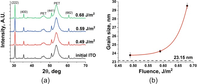
The suggestion that nanoparticle sintering is occurring due to the application of laser radiation is supported by the results of x-ray diffraction (XRD) analysis (Fig. 6(a)). As the incident laser fluence is increased, no new diffraction features appear in the pattern. However, careful examination of the strongest peak, the (222) Bragg reflection from ITO, shows that its FWHM decreases by 30% with increasing fluence from 0.59 to 0.69 Jm−2. One can then use the Scherrer equation to estimate the approximate grain size of the film components (Fig. 6(b)). It should be noted that the initial grain size calculated this way (23.15 nm) correlates well with the size of the nanoparticles used in the film deposition (~25 nm). Therefore, the increase in grain size is attributed to a corresponding increase in particle size indicating the beginnings of a sintering-based process. It should be noted that the Scherrer equation gives a lower bound for the particle size and so the possibility of the occurrence of larger polycrystalline agglomerates is not excluded by this analysis. The contribution to the XRD data from the semi-crystalline PET substrate is seen to remain unchanged during laser treatment of the overlying ITO film (see features labelled “PET” in Fig. 6(a)). This gives confirmation of by-eye observations that the substrate remains intact during the process.
Figure 6.
(a) X-ray diffraction data for ITO-based ink films on PET irradiated at the fluences indicated. The PET features remain unchanged indicating no structural decomposition of the substrate. The (222) peak associated with the ITO particles is found to narrow as the incident laser fluence is increased. Application of the Scherrer equation to this feature allows calculation of the grain size and is shown in (b). The unirradiated value of the ITO particle size based on the XRD data is 23.15 nm and compares well with the average particle size employed in the manufacture of the ink (~25 nm).
Raman Spectroscopy
Whilst the XRD data did indicate the presence of semi-crystalline PET, no features associated with the MPTS binder could be observed. As the loss of this dielectric material will have an effect on the electrical conductivity of the film, it was monitored using Raman spectroscopy (Fig. 7). The Raman spectrum of the initial ITO film turned out to largely depend on the properties of the substrate (PET). One can see that no peaks corresponding to MPTS were observed. On the other hand, the presence of the peaks corresponding to the substrate might serve as a good indicator of it remaining undamaged after laser irradiation. It can be seen that in the “working” range of fluences (i.e. where the film transmission remains relatively high) no changes in the substrate Raman spectrum happened. The absence of the D-band carbon peak in the spectrum (at around 1365 cm−1) confirms that the laser irradiation does not cause any damage to the PET film via thermal decomposition.
Figure 7.
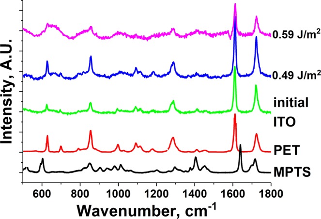
Raman spectra of the ITO films irradiated at different laser fluence values. The PET peaks remain unchanged and there is no appearance of a D-band carbon peak in the spectrum at around 1365 cm−1 supporting the conclusion that the substrate is undamaged by the process.
Electron Microscopy
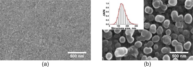
Scanning electron microscope (SEM) analysis of the unirradiated and irradiated ITO ink surface layer was performed. The SEM results (Fig. 8) show that before laser irradiation (Fig. 8(a)), the surface is smooth yet granular with any voids between ITO nanoparticles being filled with MPTS binder. At a fluence of 0.7 Jm−2, the polymer binder has largely been removed (Fig. 8(b)). Substantial change in surface morphology is observed and surface structures with transverse size of about 100–200 nm start to appear (see inset of Fig. 8(b)). This is compatible with the XRD grain size analysis which only sets a lower bound on the particle size. It is also possible that the structures observed could be interpreted as ITO nanoparticle agglomerates covered by small amounts of residual organic material. In this regime, metallic behaviour is observed in the form of low visible light transmission but increased electrical conductivity. This hinders the application of this higher fluence for devices that require light input (photovoltaics) or output (displays).
Figure 8.
SEM images of (a) the unirradiated surface of the ITO film and (b) following irradiation at a laser fluence of 0.7 Jm−2. The inset in (b) shows the transverse size distribution of the surface structures as measured from the SEM micrograph. The smooth unirradiated surface seen in (a) is found to become heavily textured in (b) as the polymer binder is removed by the laser interaction.
Conclusions
It is desirable to reduce the usage of indium in transparent conductive oxide films and also to develop processes compatible with low temperature, polymer, substrates. We have shown that gravure printing of inks based on ITO nanoparticles in a polymer binder, followed by laser irradiation, results in electrically conductive films without damage to the PET substrate. In this way, the volume of ITO used has been reduced as compared to large area sputter coating and a polymer substrate has also been able to be utilised. This has been achieved by tailoring the laser source to be strongly absorbed in the ink film whilst any light penetrating the coating is transmitted by the substrate. This reduced energy loading on the PET is also helped by minimising heat conduction during laser irradiation by restricting the laser pulse duration to the picosecond regime. The increase in conductivity due to the action of the laser light can be attributed to the removal of the dielectric MPTS binder in the ink and concomitant particle sintering. This is supported by XRD data that show an increase in grain size and SEM micrographs that indicate larger particles than in the initial sample. In order to maintain a transparency >80%, the present work has found that the sheet resistance does not go below ~300 sq−1. However, if lower transparency can be tolerated, higher laser fluences result in metal-like behaviour before damage of the film occurs and a lower value of ~50 sq−1 can be achieved, albeit at a transmittance of ~20%. The applicability of these films to flexible electronics applications is demonstrated in the Supplementary Information through bending tests.
Experimental
Equipment
A Fianium WhiteLase SC400-4 was used as the laser radiation source and has a supercontinuum spectrum ranging from 400 to 2400 nm, pulse duration of 6 ps, maximum power of 4 W and repetition rate of 40 MHz. The emission bandwidth was restricted to a narrower range by means of a dichroic mirror (Thorlabs DMLP1180) and a bandpass filter (Thorlabs FB1750-500) to achieve maximum absorption by the film without damaging the substrate. This filtered radiation was then focused by a 50 mm lens to a 45 μm diameter spot on the target surface. The sample was moved in the stationary beam using Aerotech ALS130 linear translation stages so as to raster a larger area with 25 μm line spacing (55% beam overlap). The resistivity measurements were carried out using a Jandel four-point probe system. Each resistance data point is from a treated area 3 mm × 1 mm. This allowed several resistance measurements (5 per sample) to be taken for one laser irradiated area. Other areas were irradiated in supplementary experiments (e.g. for resistivity as a function of number of pulses, or spot size) and correlation found were the parameters of these distinct studies intersected. The visible range transmission spectra were measured by a Horiba Fluoromax spectrometer. In the near infrared part of the spectrum, a Bruker IFS66 was used. An XRD diffractometer (PANalytical Empyrean) was employed to analyse the crystalline structure changes. Raman spectra of the irradiated samples were acquired by means of a Horiba iHR320 spectrometer with 532 nm excitation wavelength.
Materials and sample preparation
Initial ITO films were gravure-printed using an ITO ink which consists of crystalline nanoparticles of ITO (In2O3:Sn, 8 mol% Sn) with an average size of 25 nm, a suitable solvent and a binder. UV-curable printing inks with a 30 wt.% ITO content were prepared by dispersion of the ITO nanoparticles in an alcoholic solvent and addition of 3-methacryloxypropyl-trimethoxysilane (MPTS) as binder which was polymerised after UV irradiation16–18,51. For gravure printing a laboratory gravure printing machine (Labratester, Norbert Schläfli Maschinen, Switzerland) was used. The details of the printing process are described in16–18. The ITO coatings were dried at 70 °C for 10 min for the transport from INM to Hull before laser treatment. The final film thickness before laser irradiation was 400 nm as determined by stylus profilometry, whilst the PET substrate was 175 μm thick (Melinex® ST504).
Supplementary information
Acknowledgements
This work was conducted as part of the INFINITY project which has received funding from the European Union’s Horizon 2020 research and innovation programme under grant agreement No. 641927. Additional financial support was received from the EPSRC Centre in Laser-based Production Processes. Dr. Ali Adawi is thanked for help with the experimental equipment. Dr. Tim Prior, Dr. Khue Tian Lai, Tony Sinclair and Peter Robinson are also thanked for the XRD, IR, SEM and Raman spectra measurements respectively. Sarah Schumacher of INM - Leibniz Institute for New Materials is thanked for the fabrication of the ITO ink and for gravure printing of the ITO coatings on PET foil. Bruno Schäfer is thanked for the ellipsometry measurements.
Author Contributions
A.A.S. and H.V.S. conceived the experiments. Laser experiments were conducted by A.A.S. and material preparation was performed by T.M.A. All authors participated in analysing the data and reviewing the manuscript.
Competing Interests
The authors declare no competing interests.
Footnotes
Publisher’s note: Springer Nature remains neutral with regard to jurisdictional claims in published maps and institutional affiliations.
Electronic supplementary material
Supplementary information accompanies this paper at 10.1038/s41598-018-38043-y.
References
- 1.Brabec CJ. Organic photovoltaics: technology and market. Solar energy materials and solar cells. 2004;83:273–292. doi: 10.1016/j.solmat.2004.02.030. [DOI] [Google Scholar]
- 2.Fortunato E, Ginley D, Hosono H, Paine DC. Transparent conducting oxides for photovoltaics. MRS bulletin. 2007;32:242–247. doi: 10.1557/mrs2007.29. [DOI] [Google Scholar]
- 3.Granqvist CG, Hultåker A. Transparent and conducting ITO films: new developments and applications. Thin solid films. 2002;411:1–5. doi: 10.1016/S0040-6090(02)00163-3. [DOI] [Google Scholar]
- 4.Kim H-K, Lee S, Yun K-S. Capacitive tactile sensor array for touch screen application. Sensors and Actuators A: Physical. 2011;165:2–7. doi: 10.1016/j.sna.2009.12.031. [DOI] [Google Scholar]
- 5.Son S, Park JE, Lee J, Yang M, Kang B. Laser-assisted fabrication of single-layer flexible touch sensor. Scientific reports. 2016;6:34629. doi: 10.1038/srep34629. [DOI] [PMC free article] [PubMed] [Google Scholar]
- 6.Eritt M, May C, Leo K, Toerker M, Radehaus C. OLED manufacturing for large area lighting applications. Thin Solid Films. 2010;518:3042–3045. doi: 10.1016/j.tsf.2009.09.188. [DOI] [Google Scholar]
- 7.Kuo C, et al. Nitride-based near-ultraviolet LEDs with an ITO transparent contact. Materials Science and Engineering: B. 2004;106:69–72. doi: 10.1016/j.mseb.2003.09.018. [DOI] [Google Scholar]
- 8.Kim H, et al. Electrical, optical, and structural properties of indium–tin–oxide thin films for organic light-emitting devices. Journal of Applied Physics. 1999;86:6451–6461. doi: 10.1063/1.371708. [DOI] [Google Scholar]
- 9.Ellmer K. Past achievements and future challenges in the development of optically transparent electrodes. Nature Photonics. 2012;6:809–817. doi: 10.1038/nphoton.2012.282. [DOI] [Google Scholar]
- 10.Maruyama T, Fukui K. Indium tin oxide thin films prepared by chemical vapour deposition. Thin solid films. 1991;203:297–302. doi: 10.1016/0040-6090(91)90137-M. [DOI] [Google Scholar]
- 11.Vasu V, Subrahmanyam A. Reaction kinetics of the formation of indium tin oxide films grown by spray pyrolysis. Thin Solid Films. 1990;193:696–703. doi: 10.1016/0040-6090(90)90221-X. [DOI] [Google Scholar]
- 12.Nath P, Bunshah RF, Basol B, Staffsud O. Electrical and optical properties of In2O3:Sn films prepared by activated reactive evaporation. Thin Solid Films. 1980;72:463–468. doi: 10.1016/0040-6090(80)90532-5. [DOI] [Google Scholar]
- 13.Buchanan M, Webb J, Williams D. Preparation of conducting and transparent thin films of tin-doped indium oxide by magnetron sputtering. Applied Physics Letters. 1980;37:213–215. doi: 10.1063/1.91829. [DOI] [Google Scholar]
- 14.Wu W-F, Chiou B-S, Hsieh S-T. Effect of sputtering power on the structural and optical properties of rf magnetron sputtered ITO films. Semiconductor science and technology. 1994;9:1242. doi: 10.1088/0268-1242/9/6/014. [DOI] [Google Scholar]
- 15.Martins Amaral, T., Heusing, S., König, P. & de Oliveira, P. W. Effect of substrate temperature on morphology and resistivity of inkjet printed ITO. In Proceedings of the 11th International Conference on Coatings on Glass and Plastics (ICCG 11), 159–164 (Braunschweig, Germany, 2016).
- 16.Puetz, J., Heusing, S., de Haro Moro, M., Ahlstedt, C. M. & Aegerter, M. A. Gravure printing of transparent conducting ITO coatings for display applications. In Proc. of SPIE Vol, vol. 5963, 59631E1–59631E8 (2005).
- 17.Puetz J, Aegerter MA. Direct gravure printing of indium tin oxide nanoparticle patterns on polymer foils. Thin Solid Films. 2008;516:4495–4501. doi: 10.1016/j.tsf.2007.05.086. [DOI] [Google Scholar]
- 18.Heusing S, et al. Wet chemical deposited ITO coatings on flexible substrates for organic photodiodes. Thin Solid Films. 2009;518:1164–1169. doi: 10.1016/j.tsf.2009.06.056. [DOI] [Google Scholar]
- 19.Arias AC, MacKenzie JD, McCulloch I, Rivnay J, Salleo A. Materials and applications for large area electronics: solution-based approaches. Chemical reviews. 2010;110:3–24. doi: 10.1021/cr900150b. [DOI] [PubMed] [Google Scholar]
- 20.Dattoli EN, Lu W. ITO nanowires and nanoparticles for transparent films. Mrs Bulletin. 2011;36:782–788. doi: 10.1557/mrs.2011.212. [DOI] [Google Scholar]
- 21.Ederth J, et al. Electrical and optical properties of thin films prepared by spin coating a dispersion of nano-sized tin-doped indium oxide particles. Smart materials and structures. 2002;11:675. doi: 10.1088/0964-1726/11/5/308. [DOI] [Google Scholar]
- 22.Hwang M-s, Jeong B-y, Moon J, Chun S-K, Kim J. Inkjet-printing of indium tin oxide (ITO) films for transparent conducting electrodes. Materials Science and Engineering: B. 2011;176:1128–1131. doi: 10.1016/j.mseb.2011.05.053. [DOI] [Google Scholar]
- 23.Xia N, Gerhardt R. Fabrication and characterization of highly transparent and conductive indium tin oxide films made with different solution-based methods. Materials Research Express. 2016;3:116408. doi: 10.1088/2053-1591/3/11/116408. [DOI] [Google Scholar]
- 24.Park N-G, et al. Chemical sintering of nanoparticles: a methodology for low-temperature fabrication of dye-sensitized TiO2 films. Advanced Materials. 2005;17:2349–2353. doi: 10.1002/adma.200500288. [DOI] [Google Scholar]
- 25.Yamaguchi, T., Tobe, N., Matsumoto, D. & Arakawa, H. Highly efficient plastic substrate dye-sensitized solar cells using a compression method for preparation of TiO2 photoelectrodes. Chemical Communications 4767–4769 (2007). [DOI] [PubMed]
- 26.Miyasaka T, Kijitori Y. Low-temperature fabrication of dye-sensitized plastic electrodes by electrophoretic preparation of mesoporous TiO2 layers. Journal of the Electrochemical Society. 2004;151:A1767–A1773. doi: 10.1149/1.1796931. [DOI] [Google Scholar]
- 27.Zhang D, Yoshida T, Minoura H. Low-temperature fabrication of efficient porous titania photoelectrodes by hydrothermal crystallization at the solid/gas interface. Advanced Materials. 2003;15:814–817. doi: 10.1002/adma.200304561. [DOI] [Google Scholar]
- 28.Vaseem M, Lee S-K, Kim J-G, Hahn Y-B. Silver-ethanolamine-formate complex based transparent and stable ink: Electrical assessment with microwave plasma vs thermal sintering. Chemical Engineering Journal. 2016;306:796–805. doi: 10.1016/j.cej.2016.08.003. [DOI] [Google Scholar]
- 29.Reinhold I, et al. Argon plasma sintering of inkjet printed silver tracks on polymer substrates. Journal of Materials Chemistry. 2009;19:3384–3388. doi: 10.1039/b823329b. [DOI] [Google Scholar]
- 30.Hong S, et al. Nonvacuum, maskless fabrication of a flexible metal grid transparent conductor by low-temperature selective laser sintering of nanoparticle ink. ACS nano. 2013;7:5024–5031. doi: 10.1021/nn400432z. [DOI] [PubMed] [Google Scholar]
- 31.Zenou M, Ermak O, Saar A, Kotler Z. Laser sintering of copper nanoparticles. Journal of Physics D: Applied Physics. 2013;47:025501. doi: 10.1088/0022-3727/47/2/025501. [DOI] [Google Scholar]
- 32.Jin H-Y, et al. Rapid sintering of TiO2 photoelectrodes using intense pulsed white light for flexible dye-sensitized solar cells. Applied Physics Letters. 2014;104:143902. doi: 10.1063/1.4871370. [DOI] [Google Scholar]
- 33.Niittynen J, Sowade E, Kang H, Baumann RR, Mäntysalo M. Comparison of laser and intense pulsed light sintering (ipl) for inkjet-printed copper nanoparticle layers. Scientific reports. 2015;5:8832. doi: 10.1038/srep08832. [DOI] [PMC free article] [PubMed] [Google Scholar]
- 34.Wang B-Y, Yoo T-H, Song Y-W, Lim D-S, Oh Y-J. Cu ion ink for a flexible substrate and highly conductive patterning by intensive pulsed light sintering. ACS applied materials & interfaces. 2013;5:4113–4119. doi: 10.1021/am303268k. [DOI] [PubMed] [Google Scholar]
- 35.Hwang H-J, Chung W-H, Kim H-S. In situ monitoring of flash-light sintering of copper nanoparticle ink for printed electronics. Nanotechnology. 2012;23:485205. doi: 10.1088/0957-4484/23/48/485205. [DOI] [PubMed] [Google Scholar]
- 36.Sowade E, et al. Roll-to-roll infrared (IR) drying and sintering of an inkjet-printed silver nanoparticle ink within 1 second. Journal of Materials Chemistry C. 2015;3:11815–11826. doi: 10.1039/C5TC02291F. [DOI] [Google Scholar]
- 37.Cherrington M, et al. Ultrafast near-infrared sintering of a slot-die coated nano-silver conducting ink. Journal of Materials Chemistry. 2011;21:7562–7564. doi: 10.1039/c1jm10630a. [DOI] [Google Scholar]
- 38.Ko SH, et al. All-inkjet-printed flexible electronics fabrication on a polymer substrate by low-temperature high-resolution selective laser sintering of metal nanoparticles. Nanotechnology. 2007;18:345202. doi: 10.1088/0957-4484/18/34/345202. [DOI] [Google Scholar]
- 39.Bolduc M, Trudeau C, Beaupré P, Cloutier S, Galarneau P. Thermal dynamics effects using pulse-shaping laser sintering of printed silver inks. Scientific reports. 2018;8:1418. doi: 10.1038/s41598-018-19801-4. [DOI] [PMC free article] [PubMed] [Google Scholar]
- 40.Creighton JA, Eadon DG. Ultraviolet–visible absorption spectra of the colloidal metallic elements. Journal of the Chemical Society, Faraday Transactions. 1991;87:3881–3891. doi: 10.1039/FT9918703881. [DOI] [Google Scholar]
- 41.Tohge N, Shinmou K, Minami T. Effects of UV-irradiation on the formation of oxide thin films from chemically modified metal-alkoxides. Journal of Sol-Gel Science and Technology. 1994;2:581–585. doi: 10.1007/BF00486313. [DOI] [Google Scholar]
- 42.Zhao G, Tohge N. Preparation of photosensitive gel films and fine patterning of amorphous Al2O3-SiO2 thin films. Materials research bulletin. 1998;33:21–30. doi: 10.1016/S0025-5408(97)00188-8. [DOI] [Google Scholar]
- 43.Krug, H., Tiefensee, F., de Oliveira, P. W. & Schmidt, H. K. Organic-inorganic composite materials: Optical properties of laser-patterned and protective-coated waveguides. In Sol-Gel Optics II, vol. 1758, 448–456 (International Society for Optics and Photonics, 1992).
- 44.Park T, Kim D. Excimer laser sintering of indium tin oxide nanoparticles for fabricating thin films of variable thickness on flexible substrates. Thin Solid Films. 2015;578:76–82. doi: 10.1016/j.tsf.2015.02.015. [DOI] [Google Scholar]
- 45.Scholle, K., Lamrini, S., Koopmann, P. & Fuhrberg, P. 2 μm laser sources and their possible applications. In Frontiers in Guided Wave Optics and Optoelectronics (InTech, 2010).
- 46.Chernikov S, Zhu Y, Taylor J, Gapontsev V. Supercontinuum self-Q-switched ytterbium fiber laser. Optics Letters. 1997;22:298–300. doi: 10.1364/OL.22.000298. [DOI] [PubMed] [Google Scholar]
- 47.Pan H, et al. Fiber laser annealing of indium-tin-oxide nanoparticles for large area transparent conductive layers and optical film characterization. Applied Physics A: Materials Science & Processing. 2011;104:29–38. doi: 10.1007/s00339-011-6397-x. [DOI] [Google Scholar]
- 48.Ederth J, Heszler P, Hultåker A, Niklasson G, Granqvist C. Indium tin oxide films made from nanoparticles: models for the optical and electrical properties. Thin solid films. 2003;445:199–206. doi: 10.1016/S0040-6090(03)01164-7. [DOI] [Google Scholar]
- 49.Kanehara M, Koike H, Yoshinaga T, Teranishi T. Indium tin oxide nanoparticles with compositionally tunable surface plasmon resonance frequencies in the near-ir region. Journal of the American Chemical Society. 2009;131:17736–17737. doi: 10.1021/ja9064415. [DOI] [PubMed] [Google Scholar]
- 50.Ma K, Zhou N, Yuan M, Li D, Yang D. Tunable surface plasmon resonance frequencies of monodisperse indium tin oxide nanoparticles by controlling composition, size, and morphology. Nanoscale research letters. 2014;9:547. doi: 10.1186/1556-276X-9-547. [DOI] [PMC free article] [PubMed] [Google Scholar]
- 51.Pütz J, Al-Dahoudi N, Aegerter MA. Processing of transparent conducting coatings made with redispersible crystalline nanoparticles. Advanced Engineering Materials. 2004;6:733–737. doi: 10.1002/adem.200400078. [DOI] [Google Scholar]
Associated Data
This section collects any data citations, data availability statements, or supplementary materials included in this article.


