

Abstract
The last few decades faced on the fabrication of advanced engineering materials involving also different composites. Here, we report on the fabrication of few-layer molybdenum disulfide on top of thin polycrystalline diamond substrates with a high specific surface area. In the method, pre-deposited molybdenum coatings were sulfurized in a one-zone furnace at ambient pressure. As-prepared MoS2 layers were characterized by several techniques including grazing-incidence wide-angle X-ray scattering, atomic force microscopy, scanning electron microscopy, Raman spectroscopy and X-ray photoelectron spectroscopy. We found out that the initial thickness of Mo films determined the final c-axis crystallographic orientation of MoS2 layer as previously observed on other substrates. Even though it is well-known that Mo diffuses into diamond at elevated temperatures, the competing sulfurization applied effectively suppressed the diffusion and a chemical reaction between molybdenum and diamond. In particular, a Mo2C layer does not form at the interface between the Mo film and diamond substrate. The combination of diamond high specific surface area along with a controllable layer orientation might be attractive for applications, such as water splitting or water disinfection.
Introduction
Combination of different materials with complementary properties expands their application range and opens new possibilities for research. In this terms, the diamond and molybdenum disulfide thin films represent an attractive pair with a promising potential for sustainable technologies such as water disinfection1,2, water splitting3 or solar cells4–6.
Transition metal dichalcogenides (TMDCs) are layered materials with a formula MX2, where M and X correspond to a transition metal and chalcogen, respectively. MoS2 is recently one of the most studied TMDCs composed of covalently bonded S-Mo-S sheets which are bound by weak van der Waals forces. MoS2 is a semiconductor with an indirect bandgap of about 1.3 eV7,8, however, the monolayer MoS2 is a direct gap semiconductor with a bandgap of 1.8 eV9. This is, in particular, important for photovoltaic7 and photocatalytic8 applications due to its strong absorption in the solar spectral region.
Other applications of MoS2 include transparent and flexible field-effect transistors (FETs)10,11, photodetectors12, photovoltaic cells13,14, light-emitting diodes15 and catalysts16,17, drug delivery and biosensors18.
Diamond thin films have a great number of unique properties19–21. Indeed, its great mechanical hardness, wear resistance, chemical inertness, high thermal conductivity, optical transparency, and biocompatibility combined in one platform are advantageous for numerous application19–21. The diamond films are commonly used as protective coatings for cutting tools and sealing22,23, infrared windows and optical elements24,25, MEMS and electronic devices26,27, heater elements or heat sink28,29 and also in various bio-related researches21,30–32. In the last decade, the antibacterial effect of diamond thin films and/or diamond nanoparticles was also investigated33,34.
For MoS2 thin films, diamond may act as a mechanically stable and chemically inert carrier substrate with a high thermal conductivity which additionally can be made electrically conductive via boron doping19–21. Moreover, the surface of the diamond film can be structured to increase the surface area35,36. However, only composites of MoS2 with diamond-like carbon films have been reported to date37,38. Relatively thick films (600 nm) were fabricated by a biased target ion beam deposition technique simultaneously sputtering a MoS2 target and depositing DLC from CH4 gas37,38.
Here, we present fabrication of MoS2 thin films on diamond substrates. We are not aware of any other publication where a diamond has been used as a substrate for growing a thin MoS2 layer. We prepared MoS2 by sulfurization of thin pre-deposited Mo films with a different thickness39. In this method, a Mo film is annealed in vapors of sulfur at high temperatures converting Mo to MoS2. In the standard procedure40–42, at least two temperature regimes are employed during the synthesis. Sulfur evaporates from a powder source usually held at a temperature above the sulfur melting point. On the other hand, the Mo film must be heated to much higher temperatures to trigger the sulfurization. In our experiments, a simplified sulfurization process was used. The substrate and the sulfur powder were placed at the same position in the center of a one-zone furnace39. This enables affordable vacuum-free experimental set-up. It is important to note that the fabrication process has no impact on the diamond substrates. Molybdenum carbide (Mo2C) grows at temperatures above 550 °C from thin Mo films deposited on diamond43,44. Within the sulfurization method employed, Mo diffusion into the diamond substrate and a subsequent reaction leading to formation of molybdenum carbide was suppressed. Similarly to other substrates, it was found that the thickness of the initial Mo film determined whether the final MoS2 layer was aligned parallel or perpendicular to the substrate45–47. For the thickest MoS2 layers, well crystallized and densely packed MoS2 grains growing upright to the surface of large diamond crystallites were observed. This may have an important implication for applications deserving a large surface area.
Experimental Section
CVD synthesis of diamond thin films
Planar microcrystalline CVD diamond thin films were grown on the silicon substrate by plasma enhanced chemical vapor deposition (PE CVD) in the focused microwave plasma cavity resonator AIXTRON P6 with a deposition area up to 5 cm in diameter. The microcrystalline CVD diamond films were grown from H2/CH4/CO2 gas mixture with a flow rate of 300/15/4.5 sccm, respectively. The gas pressure was set on 60 mbar, and microwave power to 3000 W. The average temperature during 5 hour long deposition was 730 °C. The thickness of the as-prepared diamond films was 1.5 µm.
MoS2 fabrication
Firstly, molybdenum films were prepared by DC magnetron sputtering in Ar atmosphere (10−3 mbar) from a molybdenum target at room temperature. The DC power and emission current were 140 W and 0.3 A, respectively. The thickness of as-prepared Mo films was controlled by the rotation speed of a sample holder. Further, MoS2 films were prepared by sulfurization of pre-deposited Mo layers in a custom-designed CVD chamber. In particular, a Mo layer was annealed in sulfur vapors in a nitrogen atmosphere at ambient pressure. A one-zone furnace has the substrate and sulfur powder placed at the same position and temperature in the center of furnace as shown in Fig. 1.
Figure 1.
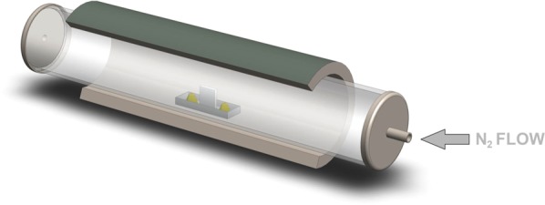
Schematic representation of the one-zone sulfurization method. A Mo coated substrate in a quartz boat is placed in the middle of the furnace along with the sulfur powder. A typical sulfur load was 3 g.
The furnace was connected to a nitrogen supply and heated at a rate of 25 °C.min−1 to the process temperature. The sulfurization temperature and time were 800 °C and 30 min, respectively. After this process step, the temperature was ramped down to 200 °C at a rate of 20 °C.min−1, followed by a spontaneous cooling.
Chemical composition analyses
Raman measurements were provided by confocal Raman microscope Alpha 300R (WiTec, Germany) using a 532 nm excitation laser line. The laser power was kept below 1 mW to avoid any beam damage. The scattered light was collected by 50× (NA = 0.8) microscope objective and detected by a cooled CCD camera. For dispersing the scattered light, a grating with 1800 gr/mm was used. The spectral resolution of the entire Raman system is about 0.75 cm−1. All the spectra were taken at ambient conditions.
XPS (X-ray photoelectron spectroscopy) spectra were recorded using Thermo Scientific K-Alpha XPS system (Thermo Fisher Scientific, UK) equipped with a micro-focused, monochromatic AlKα X-ray source (1486.6 eV). X-ray beam of 400 µm in diameter was used at 6 mA × 12 kV. The spectra were acquired in the constant analyzer energy mode with the pass energy of 200 eV for the survey. Narrow regions were collected using the snapshot acquisition mode (150 eV pass energy), enabling rapid collection of data (5 s per region). Charge compensation was achieved with the system flood gun that provides low energy electrons and low energy argon ions (20 eV) from a single source. Thermo Scientific Avantage software was used for digital acquisition and data processing. Spectral calibration was performed using an automated calibration routine and the internal Au, Ag and Cu standards.
Morphological and structural analyses
Scanning electron microscopy (SEM) was performed using FEI FEG250 with resolution of 1.2 nm equipped with SE and BSE detector. The surface morphology of the diamond and MoS2 films was probed by atomic force microscopy (AFM) in a tapping mode (Bruker, Dimension Edge), using an etched silicon probe (Bruker, RTESPA - 300).
The crystallographic structure and orientation of the films were examined by X-ray diffraction (XRD) (CuKα) in the classical Bragg–Brentano and in the grazing-incidence configuration using BRUKER AXS D8 DISCOVER diffractometer with a rotating Cu anode.
The grazing-incidence wide-angle X-ray scattering (GIWAXS) measurements were performed using Nanostar system (Bruker AXS, Germany) equipped with IμS microfocus Cu X-ray source (λ = 0.154 nm). The parallel X-ray beam after Montel optics was further collimated using evacuated pinhole collimator equipped with two 550 µm pinholes separated by 1 m. The grazing-angle of incidence of X-ray beam on the sample was set to 0.8°. Reciprocal space maps were measured using an image plate detector at a sample-to-detector distance of 80 mm. All GIWAXS measurements were performed in fully evacuated chamber.
Results and Discussion
SEM micrograph of a microcrystalline CVD diamond thin film used as a substrate for the deposition of Mo films is shown in Fig. 2a. The film consists of well faceted diamond grains with an average size of approximately 1 µm. The crystallographic orientation of the grains is random. The Raman spectrum (Fig. 2b) displays the dominant Raman active mode at 1332 cm−1 (F2g) corresponding to a vibration of the sp3 diamond lattice48.
Figure 2.
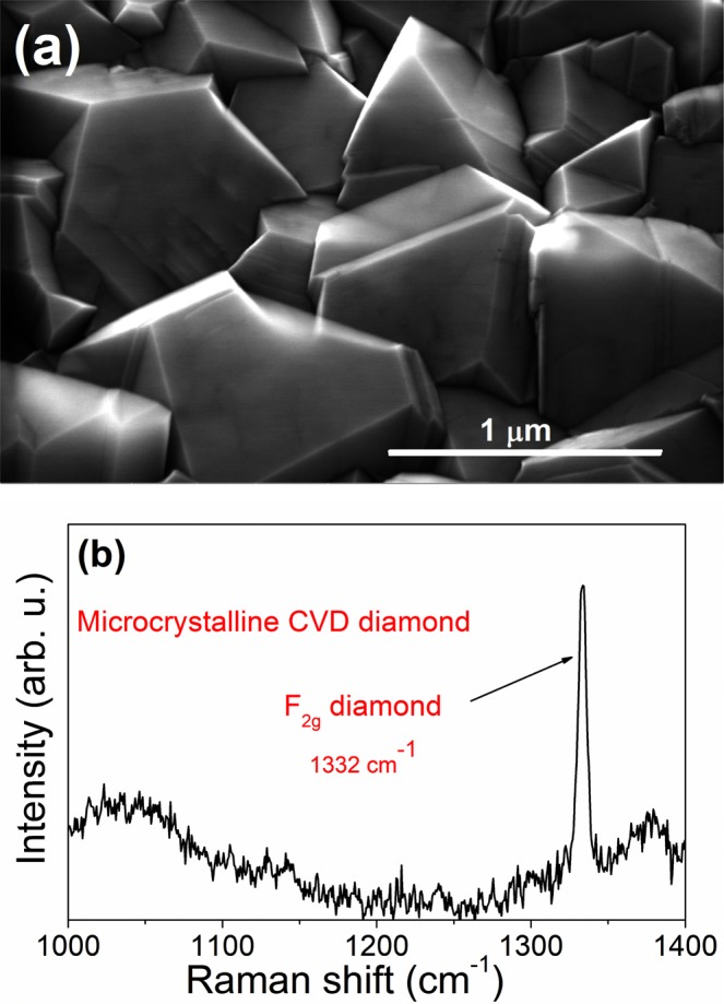
(a) SEM image and (b) Raman spectrum of a microcrystalline CVD diamond film.
SEM images of the diamond substrate after the growth of MoS2 are shown in Fig. 3. It was found that the MoS2 morphology is determined by the initial thickness of the seeding Mo film. The MoS2 layers, sulfurized from the thinnest Mo film (1 nm thick), consist from isolated or partially interconnected islands (flakes) having hexagonal shape in some cases (Fig. 3a). In the case of the 3 nm thick Mo seeding film, the as-grown layer seems to be continuous covering all the facets of the diamond substrate (Fig. 3b). Finally, the sulfurization of the thickest Mo films (6 nm) reveals a significant change in the MoS2 preferential growth mode (Fig. 3c,d). We observe thin flakes very likely standing upright on the diamond facets (Fig. 3d). With the increasing Mo thickness, we observe the transition from separated islands through continuous films to vertically aligned flakes. The initial Mo thickness plays an important role in the c-axis orientation exactly as in the case of the MoS2 films grown on the flat substrates45,47,49,50. While MoS2 grown from the thinner Mo has c-axis perpendicular to the substrate plane, the thicker Mo leads to c-axis rotated by 90°.
Figure 3.

SEM images of MoS2 layers grown from (a) 1 nm, (b) 3 nm and (c,d) 6 nm thick Mo films deposited on the microcrystalline CVD diamond substrate. In (d), standing MoS2 flakes are seen on the edge of a diamond crystallite.
Raman spectra shown in Fig. 4 confirmed the conversion of Mo to MoS2. Figure 4a displays a part of the spectrum with lines belonging to 2H-MoS2, namely the E2g mode at around 382 cm−1 and the A1g mode at ~407 cm−151. The spectra are normalized to the intensity of the A1g mode. We observe a gradual decrease of the mode’s intensity with an increasing the initial thickness of the Mo film. In agreement with the SEM images, this dependence points out to a different crystallographic unit cell alignment of the individual MoS2 layers with respect to the substrate. In contrast to thinner ones, the individual MoS2 layers may grow perpendicularly to the substrate for the thickest MoS2 layer45.
Figure 4.
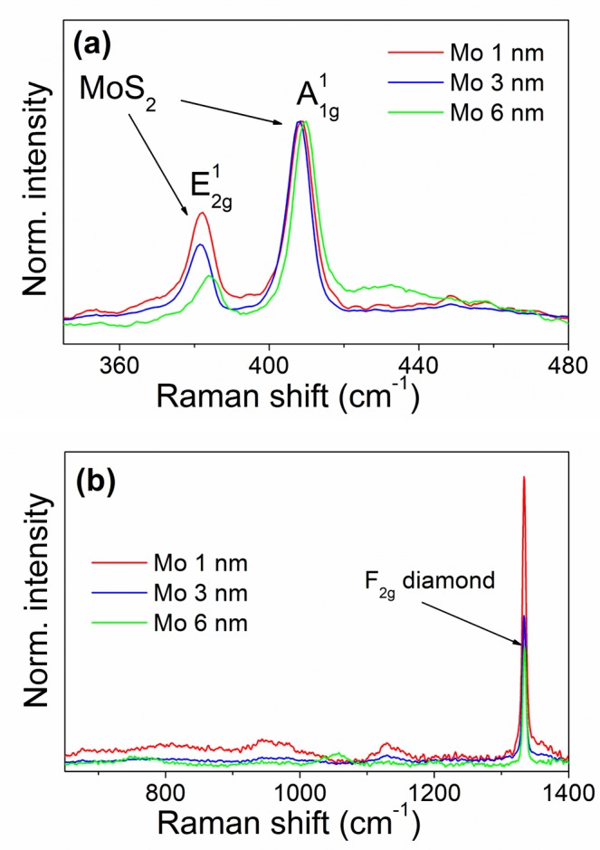
Raman spectra of MoS2 layers grown from 1, 3 and 6 nm thick Mo film on a microcrystalline CVD diamond substrate with (a) the two dominant MoS2 peaks and (b) the diamond line.
The position of the E12g line for the sample grown from the thickest Mo film is blue shifted by about 3 cm−1 compared to other samples. Also the line becomes asymmetric in shape. This is likely a consequence of the strain which both shifts the line and lifts the degeneracy of the E12g mode making it asymmetric52,53.
For the MoS2 samples having 1–6 layers, the distance between the E12g and A11g lines is a measure of the layer thickness54. However, our samples are too thick for this method to be applicable. The distance between the two lines is more than 25 cm−1 for all our samples. Even though we did not measure the actual thickness of the layers, it can be estimated from published data relating the thickness of the initial Mo film and final MoS2 layer. It was found that the latter is thicker by a factor of 3.5–4 than the former for horizontally aligned MoS2 layers45,55. This means that the MoS2 layers grown from 3 nm thick Mo films are about 10 nm thick. For vertically aligned layers, the thickness is a matter of definition. At least, it can be estimated from Fig. 3d that the MoS2 flakes are about 20 nm tall. As expected from the thickness consideration, we did not observe the photoluminescence in our samples. That is strong for monolayer MoS2 and its intensity decreases rapidly with the increasing layer thickness56,57.
As shown in Fig. 4b, besides the change in intensity, the Raman spectrum of the diamond substrate does not change with the thickness of the MoS2 layer. More important is the fact that no lines from the molybdenum carbide (Mo2C), were observed in the range between 800 and 1000 cm−1, where the Mo2C Raman lines are the most intense58,59.
Chemical states and compositions of the as-prepared MoS2 layers were analyzed by X-ray photoelectron spectroscopy (XPS). A typical spectrum taken from a MoS2 layer grown from a 3 nm Mo film is shown in Fig. 5. The Mo 3d spectral region exhibits two characteristic emission peaks at 231.1 eV (Mo 3d3/2) and 228 eV (Mo 3d5/2). The measured Mo 3d binding energies match the chemical shifts of the Mo4+ state corresponding to MoS260. Additionally, the S 2 s peak at the binding energy of 225.7 eV corresponding to MoS2 is also observed60 in this spectral region. The Mo 3d spin–orbit energy splitting of 3.1 eV is in a good agreement with the previous observations61,62. The Mo 3d core-level shift corresponding to the elemental Mo0 was not observed. However, a limited contribution of MoO3 phase was identified at the binding energies of 231.8 eV (Mo 3d5/2) and 234.8 eV (Mo 3d3/2) as shown in Fig. 5a. The observed chemical shifts of S 2p core-level states (S 2p3/2 and S 2p1/2) correspond to MoS2 (161.3 and 162.3 eV) and SO3 (166.2 and 167.6 eV).
Figure 5.
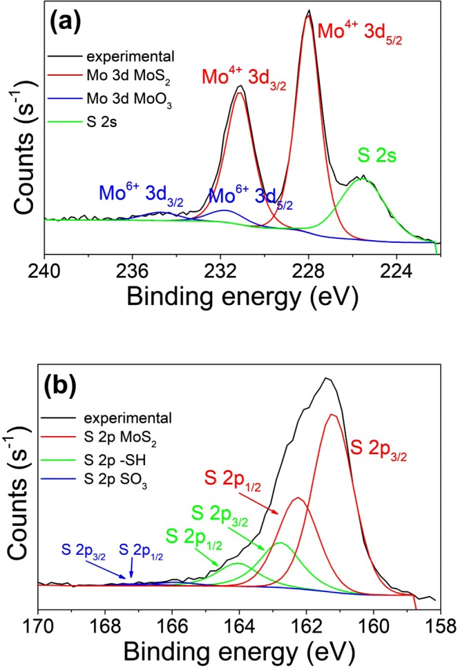
The chemical shifts of (a) Mo 3d and (b) S 2p core-level binding energies XPS spectra of a MoS2 layer grown on microcrystalline CVD diamond film. The overall spectra are deconvoluted into individual components as depicted in the spectrum.
A contribution of the thiol group (-SH) binding states is observed at 162.7 and 164.2 eV. Likely, thiol groups have partially substituted hydrogen atoms terminating the dangling bonds on the diamond surface.
Quantification of peak areas gives the atomic concentration of S and Mo in the sample. The percentage of Mo and S atoms bound in the states corresponding to MoS2 is 93% and 77%, respectively. About 21% of sulfur atoms bind to hydrogen in the thiol group.
The calculated S/Mo ratio varies from 2.2 to 2.5 and correlates with the thickness of the deposited Mo films being larger for thinner films. It is important to note that no signal due to molybdenum carbide, Mo2C, was detected in XPS spectra58,59 which is in agreement with Raman measurements.
The crystalline structure of the MoS2 layers grown on the microcrystalline CVD diamond substrates was studied by XRD. We did not register any MoS2 diffraction peaks in the layers grown from 1 nm thick Mo films. We suppose that the total amount of the MoS2 is below the detection limit of our diffractometer setup. The symmetric and grazing incidence XRD patterns of the MoS2 layers prepared from 3 nm and 6 nm thick Mo film are shown in Fig. 6a,b, respectively. XRD confirms the presence of MoS2 hexagonal 2H phase as similarly identified by Raman.
Figure 6.
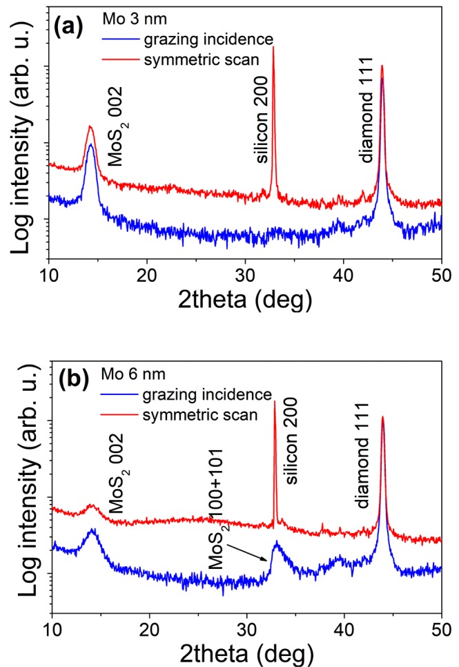
XRD patterns in symmetric (red line) and grazing-incidence (blue line) geometry of MoS2 layers prepared from (a) 3 nm and (b) 6 nm thick Mo films. Diffraction peaks of MoS2, silicon and diamond are indexed in the figures.
The comparable intensities of 111 diamond diffractions measured in symmetric and grazing-incidence geometries confirm untextured polycrystalline diamond film. On the other hand, the significant intensity changes of 002 MoS2 diffractions found between the two employed XRD measurement geometries imply the growth of a textured MoS2 film on the top of polycrystalline diamond substrate. As shown in Fig. 6, the intensity of the 002 diffraction peak is weaker for MoS2 layers grown from a thicker Mo film than that for the 3 nm Mo one. This means that increasing the Mo thickness the crystallographic orientation of the MoS2 layers with respect to diamond substrate is changing.
Conversely, the change of the MoS2 layer alignment makes other diffractions detectable as confirmed by an appearance of the 100 and 101 diffractions in a grazing incidence measurement. In order to explain these observations, we additionally performed grazing-incidence wide-angle X-ray scattering (GIWAXS) measurements. This method is suitable for studying the crystallographic orientation of thin polycrystalline films63. In contrast to HRTEM (high resolution transmission electron microscopy), which is a rather local probe, GIWAXS technique provides a statistical average over the whole sample area. Moreover, no special sample preparation is necessary.
The GIWAXS reciprocal space maps of the sulfurized 3 and 6 nm Mo films are shown in Fig. 7a,b, respectively. The diffraction ring at q ~ 3 Å−1 belongs to 111 diffraction of diamond phase. The most intense 002 diffraction of MoS2 is located at 1 Å−1. The two less intense 100 and 103 diffractions can be found at 2.3 and 2.7 Å−1, respectively. The 101 diffraction merges with 100 on the scale used in the figure.
Figure 7.

GIWAXS reciprocal space maps of MoS2 layers prepared from Mo films with the nominal thickness of (a) 3 nm and (b) 6 nm The intensities are normalized to a diamond 111 diffraction.
The MoS2 layers exhibit a uniaxial texture with the crystallographic c-axis aligned along the substrate surface normal (Fig. 7a) for layers grown from 3 nm thick Mo. On the other hand, the c-axis is perpendicular to the surface normal (Fig. 7b) for layers grown from 6 nm Mo as validated by the oriented 002 partial diffraction rings. The apparent moderate orientation degree of crystallographic c-axis has an origin in large angular spread of underlying polycrystalline diamond facets as explained below.
The influence of initial Mo thickness on the crystallographic orientation was already observed in the case of MoS2 films prepared on flat substrates45,47,49,50. The results of our GIWAXS measurements validate the same behavior also for MoS2 layers grown on rough CVD diamond.
For deeper understanding, we have also used AFM to determine the angular distribution of the diamond facets supporting the thin MoS2 layers. Figure 8a shows the AFM image of the microcrystalline CVD diamond film. Figure 8b shows the calculated distribution of the inclination angles of diamond facets64. The θf angle, plotted on the x-axis, corresponds to the angle between the normal of the substrate and the normal of diamond facets, i.e. the angle between the substrate plane and the surface of the diamond. The y-axis represents the normalized angular density of diamond facets having the inclination angle θf. The angular distribution is well described by the bi-Gaussian distribution function (Fig. 8b) having the maximum at approximately 15°.
Figure 8.
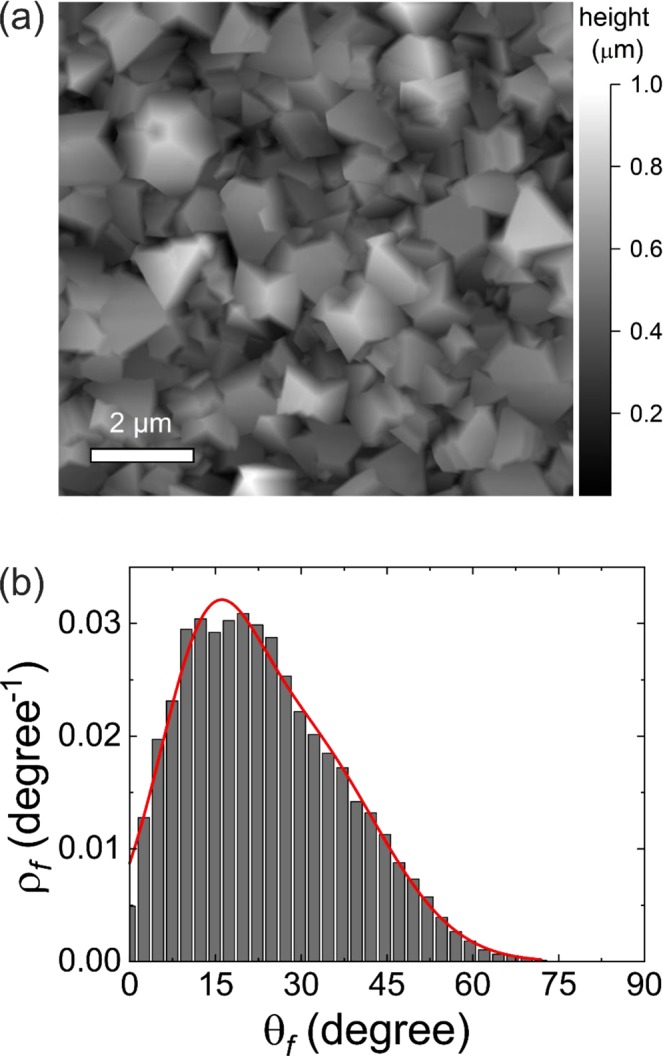
(a) AFM micrograph of the microcrystalline CVD diamond surface and (b) the corresponding distribution of inclinations of the diamond facets. The red curve shows the bi-Gaussian fit of the angular distribution of diamond facets.
It is obvious, that although the diamond films have no preferential crystallographic orientation, the measured angular deviations of the diamond facets from the substrate plane will have a pronounced effect on the GIWAXS texture measurements. Indeed, this is in a good agreement with the 002 diffracted intensity distributions in the GIWAXS measurements for the vertically and horizontally grown MoS2 layers (Fig. 7). The angular distribution of the diamond facets gives rise to smeared intensity distributions along the 002 diffraction ring with the maximum at qz and qxy for the horizontally (3 nm Mo) and vertically (6 nm Mo) grown MoS2 layers, respectively.
Based on SEM and GIWAXS results, we propose the following growth modes for the formation of a MoS2 film. Figure 9 shows a schematic representation of anticipated growth of MoS2 layers depending on the initial thicknesses of the Mo seeding. Using the 1 nm Mo, we observed a dominant horizontal growth of discontinuous MoS2 layers as concluded from SEM and Raman measurements (Fig. 9a). As the Mo film thickness increases to 3 nm, the diamond substrate is horizontally grown with MoS2 layers covering all its surface. To note, we identified also certain areas where a combination of the simultaneous horizontal and vertical growth was evidenced (Fig. 9b). This is in a good agreement with the results obtained from GIWAXS measurements. Finally, employing the Mo thickness of 6 nm induced the dominance of vertically grown MoS2 layers (Fig. 9c).
Figure 9.
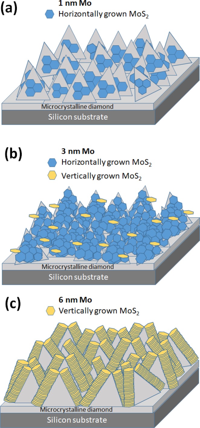
Schematic representation of MoS2 layers grown from films of different Mo thickness on the top of the microcrystalline CVD diamond films.
Up to now, a detailed growth mechanism of the MoS2 films prepared by the sulfurization of pre-deposited Mo films is still under discussion. Firstly, the sulfur starts to form the MoS2 layers on the top of the Mo films. In such a case, the conventional bottom-up mechanism (as in the case of one-step methods e.g. pulsed laser deposition51) is not applicable. When the Mo thickness exceeds a critical threshold thickness, 6 nm in our case, the vertical growth of MoS2 occurs exclusively. Jung et al.45 have found that the thickness of the initial Mo film is indeed the critical parameter that dictates the preferential orientation of the MoS2 layers. However, the identification of exact threshold thickness is still uncertain. Even though the nominal thickness of the as-deposited Mo films was 1, 3 and 6 nm, the surface morphology of the diamond film (Fig. 2a) may locally decrease the thickness of the Mo films65. The self-shadowing effect is naturally present due to the uneven substrate features and as a result of a directional Mo vapor flux66. Consequently, the thickness of a deposited Mo film varies locally due to preferential deposition of the incident Mo atoms on higher surface points67. To distinguish the value more certainly, atomically flat substrates has to be used.
In sum our study confirms that the MoS2 growth on the well-faceted and rough diamond thin films can be simply tailored just by tuning the thickness of a pre-deposited Mo films. This technological issue can be crucial especially for applications where vertically aligned MoS2 layers are required1.
Conclusion
Few-layer MoS2 were prepared on microcrystalline CVD diamond substrates by sulfurization of pre-deposited Mo films. In the course of sulfurization, Mo coated substrates and sulfur powder were placed close to each other in a one-zone furnace and exposed to the same temperature so an additional control over the sulfur temperature was not needed. As a results of this particular experimental design, the sulfur-rich environment during the process and diffusion of sulfur into molybdenum at temperatures below that required for formation of molybdenum carbide prevents the formation of the latter at the Mo-diamond interface. This finding may open a way for growing MoS2 layers on substrates which are otherwise susceptible to a chemical reaction with molybdenum. We have also demonstrated a horizontal and vertical growth of MoS2 layers, in terms of crystallographic c-axis orientation, by tuning the Mo film thickness. The combination of diamond unique properties and MoS2 ultra-thin layers with a tunable crystallographic orientation can offer material properties relevant for a wide range of applications.
Acknowledgements
This work was supported by the Slovak Research and Development Agency, APVV-15-0693, APVV-15-0641, APVV-16-0319, APVV-17-0352, Slovak Grant Agency for Science, VEGA 2/0149/17, P108/12/G108 and SASPRO Programme project 0068/01/01, co-financed by the European Union and the Slovak Academy of Science. We acknowledge Ján Dérer for the deposition of molybdenum films.
Author Contributions
M.S. performed the experimental syntheses and characterizations of MoS2 layers; O.B., T.I., G.V. and A.K. performed synthesis and characterization of diamond films; E.D. performed XRD measurements; P.S., J.H. and E.M. performed the Giwaxs measurements and interpretation of the results; N.M. performed the AFM measurements and determination of the angular distribution in diamond films; M.H. performed the Raman characterization; M.S. and M.H. supervised the project and wrote the manuscript. All authors discussed the results and commented on the manuscript.
Competing Interests
The authors declare no competing interests.
Footnotes
Publisher’s note: Springer Nature remains neutral with regard to jurisdictional claims in published maps and institutional affiliations.
References
- 1.Liu C, et al. Rapid water disinfection using vertically aligned MoS2 nanofilms and visible light. Nature Nanotechnology. 2016;11:1098–1104. doi: 10.1038/nnano.2016.138. [DOI] [PubMed] [Google Scholar]
- 2.Massey AT, Gusain R, Kumari S, Khatri OP. Hierarchical Microspheres of MoS2 Nanosheets: Efficient and Regenerative Adsorbent for Removal of Water-Soluble Dyes. Industrial & Engineering Chemistry Research. 2016;55:7124–7131. doi: 10.1021/acs.iecr.6b01115. [DOI] [Google Scholar]
- 3.Xu J, Cao X. Characterization and mechanism of MoS2/CdS composite photocatalyst used for hydrogen production from water splitting under visible light. Chemical Engineering Journal. 2015;260:642–648. doi: 10.1016/j.cej.2014.07.046. [DOI] [Google Scholar]
- 4.Singh E, Kim KS, Yeom GY, Nalwa HS. Atomically Thin-Layered Molybdenum Disulfide (MoS2) for Bulk-Heterojunction Solar Cells. ACS Applied Materials & Interfaces. 2017;9:3223–3245. doi: 10.1021/acsami.6b13582. [DOI] [PubMed] [Google Scholar]
- 5.Tsai M-L, et al. Monolayer MoS2 Heterojunction Solar Cells. ACS Nano. 2014;8:8317–8322. doi: 10.1021/nn502776h. [DOI] [PubMed] [Google Scholar]
- 6.Hao LZ, et al. High-performance n-MoS2/i-SiO2/p-Si heterojunction solar cells. Nanoscale. 2015;7:8304–8308. doi: 10.1039/C5NR01275A. [DOI] [PubMed] [Google Scholar]
- 7.Gourmelon E, et al. MS2 (M = W, Mo) photosensitive thin films for solar cells. Solar Energy Materials and Solar Cells. 1997;46:115–121. doi: 10.1016/S0927-0248(96)00096-7. [DOI] [Google Scholar]
- 8.Ho W, Yu JC, Lin J, Yu J, Li P. Preparation and Photocatalytic Behavior of MoS2 and WS2 Nanocluster Sensitized TiO2. Langmuir. 2004;20:5865–5869. doi: 10.1021/la049838g. [DOI] [PubMed] [Google Scholar]
- 9.Mak KF, Lee C, Hone J, Shan J, Heinz TF. Atomically Thin MoS2: A New Direct-Gap Semiconductor. Physical Review Letters. 2010;105:136805. doi: 10.1103/PhysRevLett.105.136805. [DOI] [PubMed] [Google Scholar]
- 10.Kashid RV, et al. Enhanced Field-Emission Behavior of Layered MoS2 Sheets. Small. 2013;9:2730–2734. doi: 10.1002/smll.201300002. [DOI] [PubMed] [Google Scholar]
- 11.Kim S, et al. High-mobility and low-power thin-film transistors based on multilayer MoS2 crystals. Nature Communications. 2012;3:1011. doi: 10.1038/ncomms2018. [DOI] [PubMed] [Google Scholar]
- 12.Lopez-Sanchez O, Lembke D, Kayci M, Radenovic A, Kis A. Ultrasensitive photodetectors based on monolayer MoS2. Nature Nanotechnology. 2013;8:497–501. doi: 10.1038/nnano.2013.100. [DOI] [PubMed] [Google Scholar]
- 13.Bernardi M, Palummo M, Grossman JC. Extraordinary Sunlight Absorption and One Nanometer Thick Photovoltaics Using Two-Dimensional Monolayer Materials. Nano Letters. 2013;13:3664–3670. doi: 10.1021/nl401544y. [DOI] [PubMed] [Google Scholar]
- 14.Fontana M, et al. Electron-hole transport and photovoltaic effect in gated MoS2 Schottky junctions. Scientific Reports. 2013;3:1634. doi: 10.1038/srep01634. [DOI] [PMC free article] [PubMed] [Google Scholar]
- 15.Britnell L, et al. Strong Light-Matter Interactions in Heterostructures of Atomically Thin Films. Science. 2013;340:1311–1314. doi: 10.1126/science.1235547. [DOI] [PubMed] [Google Scholar]
- 16.Chang Y-H, et al. Highly Efficient Electrocatalytic Hydrogen Production by MoSx Grown on Graphene-Protected 3D Ni Foams. Advanced Materials. 2013;25:756–760. doi: 10.1002/adma.201202920. [DOI] [PubMed] [Google Scholar]
- 17.Chang Y-H, et al. Three-Dimensional Molybdenum Sulfide Sponges for Electrocatalytic Water Splitting. Small. 2014;10:895–900. doi: 10.1002/smll.201302407. [DOI] [PubMed] [Google Scholar]
- 18.Tang, K. et al. Molybdenum disulfide (MoS2) nanosheets vertically coated on titanium for disinfection in the dark. Arabian Journal of Chemistry, 10.1016/j.arabjc.2017.12.013 (2017).
- 19.May PW. Diamond thin films: a 21st-century material. Philosophical Transactions of the Royal Society A: Mathematical, Physical and Engineering Sciences. 2000;358:473–495. doi: 10.1098/rsta.2000.0542. [DOI] [Google Scholar]
- 20.Kalish R. Diamond as a unique high-tech electronic material: difficulties and prospects. Journal of Physics D: Applied Physics. 2007;40:6467–6478. doi: 10.1088/0022-3727/40/20/S22. [DOI] [Google Scholar]
- 21.Amaral, M. Biotribology and biological behaviour of nanocrystalline diamond (NCD) coatings for medical applications. In Diamond-Based Materials for Biomedical Applications 48–70, 10.1533/9780857093516.1.48 (Elsevier, 2013).
- 22.Hollman P, Björkman H, Alahelisten A, Hogmark S. Diamond coatings applied to mechanical face seals. Surface and Coatings Technology. 1998;105:169–174. doi: 10.1016/S0257-8972(98)00481-2. [DOI] [Google Scholar]
- 23.Grögler T, Plewa O, Rosiwal SM, Singer RF. CVD diamond films as protective coatings on titanium alloys. International Journal of Refractory Metals and Hard Materials. 1998;16:217–222. doi: 10.1016/S0263-4368(98)00021-3. [DOI] [Google Scholar]
- 24.Koidl P, Klages C-P. Optical applications of polycrystalline diamond. Diamond and Related Materials. 1992;1:1065–1074. doi: 10.1016/0925-9635(92)90076-Z. [DOI] [Google Scholar]
- 25.Bachmann PK, Wiechert DU. Optical characterization of diamond. Diamond and Related Materials. 1992;1:422–433. doi: 10.1016/0925-9635(92)90141-A. [DOI] [Google Scholar]
- 26.Kohn E, Gluche P, Adamschik M. Diamond MEMS — a new emerging technology. Diamond and Related Materials. 1999;8:934–940. doi: 10.1016/S0925-9635(98)00294-5. [DOI] [Google Scholar]
- 27.Denisenko A, Kohn E. Diamond power devices. Concepts and limits. Diamond and Related Materials. 2005;14:491–498. doi: 10.1016/j.diamond.2004.12.043. [DOI] [Google Scholar]
- 28.Seelmann-Eggebert M, et al. Heat-spreading diamond films for GaN-based high-power transistor devices. Diamond and Related Materials. 2001;10:744–749. doi: 10.1016/S0925-9635(00)00562-8. [DOI] [Google Scholar]
- 29.Baek SS, Choi B, Oh Y. Design of a high-density thermal inkjet using heat transfer from CVD diamond. Journal of Micromechanics and Microengineering. 2004;14:750–760. doi: 10.1088/0960-1317/14/5/014. [DOI] [Google Scholar]
- 30.Nebel CE, et al. Diamond and biology. Journal of The Royal Society Interface. 2007;4:439–461. doi: 10.1098/rsif.2006.0196. [DOI] [PMC free article] [PubMed] [Google Scholar]
- 31.Bajaj P, et al. Ultrananocrystalline diamond film as an optimal cell interface for biomedical applications. Biomedical Microdevices. 2007;9:787–794. doi: 10.1007/s10544-007-9090-2. [DOI] [PubMed] [Google Scholar]
- 32.Bergonzo P, et al. 3D shaped mechanically flexible diamond microelectrode arrays for eye implant applications: The MEDINAS project. IRBM. 2011;32:91–94. doi: 10.1016/j.irbm.2011.01.032. [DOI] [Google Scholar]
- 33.Medina O, et al. Bactericide and bacterial anti-adhesive properties of the nanocrystalline diamond surface. Diamond and Related Materials. 2012;22:77–81. doi: 10.1016/j.diamond.2011.12.022. [DOI] [Google Scholar]
- 34.Budil J, et al. Anti-adhesive properties of nanocrystalline diamond films against Escherichia coli bacterium: Influence of surface termination and cultivation medium. Diamond and Related Materials. 2018;83:87–93. doi: 10.1016/j.diamond.2018.02.001. [DOI] [Google Scholar]
- 35.Davydova M, et al. Fabrication of diamond nanorods for gas sensing applications. Applied Surface Science. 2010;256:5602–5605. doi: 10.1016/j.apsusc.2010.03.034. [DOI] [Google Scholar]
- 36.Kozak H, et al. Nanostructured Diamond Layers Enhance the Infrared Spectroscopy of Biomolecules. Langmuir. 2014;30:2054–2060. doi: 10.1021/la404814c. [DOI] [PubMed] [Google Scholar]
- 37.Niakan H, Zhang C, Hu Y, Szpunar JA, Yang Q. Thermal stability of diamond-like carbon–MoS2 thin films in different environments. Thin Solid Films. 2014;562:244–249. doi: 10.1016/j.tsf.2014.04.068. [DOI] [Google Scholar]
- 38.Niakan H, Zhang C, Yang L, Yang Q, Szpunar JA. Structure and properties of DLC–MoS2 thin films synthesized by BTIBD method. Journal of Physics and Chemistry of Solids. 2014;75:1289–1294. doi: 10.1016/j.jpcs.2014.07.002. [DOI] [Google Scholar]
- 39.Sojkova, M. et al. MoS2 thin films prepared by sulfurization. in (eds Campo, E. M., Dobisz, E. A. & Eldada, L. A.) 56, 10.1117/12.2273846 (SPIE, 2017).
- 40.Orofeo CM, Suzuki S, Sekine Y, Hibino H. Scalable synthesis of layer-controlled WS2 and MoS2 sheets by sulfurization of thin metal films. Applied Physics Letters. 2014;105:083112. doi: 10.1063/1.4893978. [DOI] [Google Scholar]
- 41.Yim C, et al. Investigation of the optical properties of MoS2 thin films using spectroscopic ellipsometry. Applied Physics Letters. 2014;104:103114. doi: 10.1063/1.4868108. [DOI] [Google Scholar]
- 42.Wu C-R, Chang X-R, Wu C-H, Lin S-Y. The Growth Mechanism of Transition Metal Dichalcogenides by using Sulfurization of Pre-deposited Transition Metals and the 2D Crystal Hetero-structure Establishment. Scientific Reports. 2017;7:42146. doi: 10.1038/srep42146. [DOI] [PMC free article] [PubMed] [Google Scholar]
- 43.Mikhailov SN, et al. The behaviour of the molybdenum-CVD diamond interface at high temperature. Diamond and Related Materials. 1995;4:1137–1141. doi: 10.1016/0925-9635(95)00289-8. [DOI] [Google Scholar]
- 44.Yeh JJ, Pfeffer RL, Cole MW, Ohring M, Yehoda JE. Reactions between tungsten and molybdenum thin films and polycrystalline diamond substrates. Diamond and Related Materials. 1996;5:1195–1203. doi: 10.1016/0925-9635(96)00528-6. [DOI] [Google Scholar]
- 45.Jung Y, et al. Metal Seed Layer Thickness-Induced Transition From Vertical to Horizontal Growth of MoS2 and WS2. Nano Letters. 2014;14:6842–6849. doi: 10.1021/nl502570f. [DOI] [PubMed] [Google Scholar]
- 46.Kong D, et al. Synthesis of MoS2 and MoSe2 Films with Vertically Aligned Layers. Nano Letters. 2013;13:1341–1347. doi: 10.1021/nl400258t. [DOI] [PubMed] [Google Scholar]
- 47.Cho S-Y, et al. Highly Enhanced Gas Adsorption Properties in Vertically Aligned MoS2 Layers. ACS Nano. 2015;9:9314–9321. doi: 10.1021/acsnano.5b04504. [DOI] [PubMed] [Google Scholar]
- 48.Solin SA, Ramdas AK. Raman Spectrum of Diamond. Physical Review B. 1970;1:1687–1698. doi: 10.1103/PhysRevB.1.1687. [DOI] [Google Scholar]
- 49.Hu T, et al. Oxidation-Sulfidation Approach for Vertically Growing MoS2 Nanofilms Catalysts on Molybdenum Foils as Efficient HER Catalysts. The Journal of Physical Chemistry C. 2016;120:25843–25850. doi: 10.1021/acs.jpcc.6b08120. [DOI] [Google Scholar]
- 50.Stern, C. et al. Growth Mechanisms and Electronic Properties of Vertically Aligned MoS2. Scientific Reports8 (2018). [DOI] [PMC free article] [PubMed]
- 51.Siegel G, Venkata Subbaiah YP, Prestgard MC, Tiwari A. Growth of centimeter-scale atomically thin MoS2 films by pulsed laser deposition. APL Materials. 2015;3:056103. doi: 10.1063/1.4921580. [DOI] [Google Scholar]
- 52.Michail A, Delikoukos N, Parthenios J, Galiotis C, Papagelis K. Optical detection of strain and doping inhomogeneities in single layer MoS2. Applied Physics Letters. 2016;108:173102. doi: 10.1063/1.4948357. [DOI] [Google Scholar]
- 53.Wurstbauer U, Miller B, Parzinger E, Holleitner AW. Light–matter interaction in transition metal dichalcogenides and their heterostructures. Journal of Physics D: Applied Physics. 2017;50:173001. doi: 10.1088/1361-6463/aa5f81. [DOI] [Google Scholar]
- 54.Lee C, et al. Anomalous Lattice Vibrations of Single- and Few-Layer MoS2. ACS Nano. 2010;4:2695–2700. doi: 10.1021/nn1003937. [DOI] [PubMed] [Google Scholar]
- 55.Li D, et al. Optical properties of thickness-controlled MoS2 thin films studied by spectroscopic ellipsometry. Applied Surface Science. 2017;421:884–890. doi: 10.1016/j.apsusc.2016.09.069. [DOI] [Google Scholar]
- 56.Splendiani A, et al. Emerging Photoluminescence in Monolayer MoS2. Nano Letters. 2010;10:1271–1275. doi: 10.1021/nl903868w. [DOI] [PubMed] [Google Scholar]
- 57.Eda G, et al. Photoluminescence from Chemically Exfoliated MoS2. Nano Letters. 2011;11:5111–5116. doi: 10.1021/nl201874w. [DOI] [PubMed] [Google Scholar]
- 58.Pan LF, et al. Molybdenum carbide stabilized on graphene with high electrocatalytic activity for hydrogen evolution reaction. Chem. Commun. 2014;50:13135–13137. doi: 10.1039/C4CC05698A. [DOI] [PubMed] [Google Scholar]
- 59.Xiao T-C, et al. Preparation and Characterisation of Bimetallic Cobalt and Molybdenum Carbides. Journal of Catalysis. 2001;202:100–109. doi: 10.1006/jcat.2001.3247. [DOI] [Google Scholar]
- 60.Deokar G, Vignaud D, Arenal R, Louette P, Colomer J-F. Synthesis and characterization of MoS2 nanosheets. Nanotechnology. 2016;27:075604. doi: 10.1088/0957-4484/27/7/075604. [DOI] [PubMed] [Google Scholar]
- 61.Zhan Y, Liu Z, Najmaei S, Ajayan PM. & Lou, J. Large-Area Vapor-Phase Growth and Characterization of MoS2 Atomic Layers on a SiO2 Substrate. Small. 2012;8:966–971. doi: 10.1002/smll.201102654. [DOI] [PubMed] [Google Scholar]
- 62.Lu C, Liu W, Li H, Tay BK. A binder-free CNT network–MoS2 composite as a high performance anode material in lithium ion batteries. Chem. Commun. 2014;50:3338–3340. doi: 10.1039/C3CC49647C. [DOI] [PubMed] [Google Scholar]
- 63.Widjonarko N. Introduction to Advanced X-ray Diffraction Techniques for Polymeric Thin Films. Coatings. 2016;6:54. doi: 10.3390/coatings6040054. [DOI] [Google Scholar]
- 64.Nečas D, Klapetek P. Gwyddion: an open-source software for SPM data analysis. Open Physics. 2012;10:181–188. doi: 10.2478/s11534-011-0096-2. [DOI] [Google Scholar]
- 65.Pelliccione, M. & Lu, T.-M. Evolution of thin film morphology: modeling and simulations. (Springer, 2008).
- 66.Zhao Y. Dynamic Shadowing Growth and Its Energy Applications. Frontiers in Energy Research. 2014;2:38. doi: 10.3389/fenrg.2014.00038. [DOI] [Google Scholar]
- 67.Karabacak T. Thin-film growth dynamics with shadowing and re-emission effects. Journal of Nanophotonics. 2011;5:052501. doi: 10.1117/1.3543822. [DOI] [Google Scholar]