Abstract
Semiconductor nanowires can act as nanoscaled optical fibers, enabling them to guide and concentrate light emitted by surface-bound fluorophores, potentially enhancing the sensitivity of optical biosensing. While parameters such as the nanowire geometry and the fluorophore wavelength can be expected to strongly influence this lightguiding effect, no detailed description of their effect on in-coupling of fluorescent emission is available to date. Here, we use confocal imaging to quantify the lightguiding effect in GaP nanowires as a function of nanowire geometry and light wavelength. Using a combination of finite-difference time-domain simulations and analytical approaches, we identify the role of multiple waveguide modes for the observed lightguiding. The normalized frequency parameter, based on the step-index approximation, predicts the lightguiding ability of the nanowires as a function of diameter and fluorophore wavelength, providing a useful guide for the design of optical biosensors based on nanowires.
Keywords: Nanowires, III−V, fluorescence, confocal microscopy, biosensing, waveguiding
The use of vertical, elongated nanostructures such as nanopillars,1 nanowires,2 and carbon nanotubes3 for biosensing applications has been the subject of several recent studies.4,5 One motivation is their high surface-area-to-footprint ratio, which is typically beneficial for signal enhancing in biosensing by effectively increasing the available sensing area.
Notably, semiconductor nanowires have attracted significant interest for biosensing because of their electrical properties, in particular in the context of nanowire-based field effect transistor (FET) sensors.6,7 Numerous reports discuss the interactions of nanowires with biomolecules such as proteins,8 model membranes,9 and even living cells.10 Given the importance of fluorescence-based techniques in biological imaging, the optical properties of nanowires are also of interest. These structures can potentially enhance the performance of a large class of biosensing applications in combination with fluorescence microscopy, for example to characterize the binding rate of biomolecules on a surface.
Recent works reported potential ways to enhance biosensing based on fluorescent biomolecules by using lightguiding properties of nanowires.11 Light emitted by fluorophores bound to the nanowire surface can couple into the nanowire core due to near-field interactions, as in an optical fiber.12 In a free-standing nanowire, light can be guided to its tip, regardless of the fluorophore position along the nanowire length. Harnessing this effect would potentially allow nanowires to be used as signal integrators for the fluorescence generated close to their surface,13 thereby increasing the signal-to-noise ratio.11,14,15 This lightguiding effect, in addition to the high surface-area-to-footprint ratio, makes nanowires excellent candidates for improving the detection of low-level fluorescence signals.
The waveguiding properties of semiconductor nanowires have been previously extensively studied in the context of nanowire lasing,16−18 LEDs,19 and nanowire-based solar cells.20,21 Waveguiding in nanowires depends on both nanowire diameter and light wavelength, and efficient waveguiding has been shown to manifest only above a threshold diameter.22 Coupling in multiple waveguide modes has also been extensively reported in nanowire lasers.23−25 It is then reasonable to expect that a nanowire’s ability to guide light emitted by a surface-bound fluorophore will strongly depend on the waveguide modes it can support, and therefore on its geometry, as well as on the fluorophore emission.
However, in order to be able to design an efficient, nanowire-based optical biosensor, it is necessary to fully assess their lightguiding properties as a function of relevant parameters and for the specific case of surface-bound fluorophores. Unlike lasers, fluorophore emission is not coherent and its bandwidth spans over tens of nm. The wide emission spectra of fluorophores, together with the frequent use of multiple fluorescent dyes in the same assay, makes it imperative to collect as much light as possible over a large wavelength interval in the visible spectrum. Moreover, fluorophores are located outside the nanowire boundaries, meaning that in-coupling can only happen in partially localized modes.
Although the in-coupling of fluorophores has recently been observed in a variety of III–V nanowires, such as GaP,11 GaAs,15 and InAs,14 the dependence on fluorophore emission wavelength has been experimentally addressed only for a specific nanowire diameter,14 and no detailed account of multimode in-coupling of fluorophore emission in nanowires is available to date.
Here, we present a comprehensive description of the lightguiding effect’s dependence on a broad range of nanowire diameters (50–260 nm) and fluorophore emission wavelengths (520–650 nm) and show that higher-order waveguide modes are essential to understand and predict the in-coupling and guiding of light for biosensing applications.
We used confocal microscopy to excite and detect the emission signals of fluorophores attached to nanowires and to determine the profile of fluorescence intensity along the length of the nanowire.14 Lightguiding nanowires show an increased signal at the nanowire tip, consistent with previous studies,14 while we detect a near-constant emission intensity profile along the nanowire length when no lightguiding takes place. After quantifying the strength of the lightguiding effect, we use finite-difference time domain simulations to interpret our experiments in terms of multiple waveguide modes. Furthermore, we establish that the normalized frequency parameter, used in the context of optical fibers, can be used to predict the lightguiding effect.
In this study, we chose to work with GaP nanowires, due to the indirect bandgap of GaP at 2.26 eV, which leads to negligible absorption in most of the visible wavelength range. Moreover, GaP is known to be biocompatible,26,27 increasing the range of its possible applications for biosensing, including in vivo studies using optical microscopy.
GaP nanowires were grown using metal–organic vapor phase epitaxy from seed Au particles deposited in square arrays (Figure 1a) on a GaP substrate (see Supporting Information Section 1 for experimental details). Nanowires were spaced by 1 μm, which, according to theoretical modeling, is sufficient to optically decouple the nanowires from one another and thus allows us to analyze each nanowire as an individual optical object.28 Using a combination of axial and axial/radial growth from Au seed disks of varying sizes, we obtained a range of GaP nanowires samples with diameters d = 50, 100, 130, 160, 175, 195, 210, and 260 nm and 3–4 μm in length (see Supporting Information Section 1 for details). Nanowires were subsequently coated with 10 nm of alumina (Al2O3) using atomic layer deposition to facilitate further functionalization, as described below (Figure 1b). Our modeling shows that the waveguiding properties of the nanowires depend primarily on the diameter d of the GaP core. Therefore, in the following, we identify nanowires by their GaP core diameter.
Figure 1.
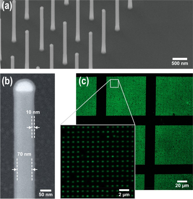
(a) SEM image of a GaP nanowire array (1 μm spacing, d = 100 nm). (b) SEM image of a single nanowire, coated with 10 nm of Al2O3. Nanowire diameter, d, is defined by the core GaP diameter (in this case 70 nm). (c) Confocal xy slice of A488-labeled nanowire array (1 μm spacing, d = 50 nm), at two different magnifications.
Nanowires were functionalized with biotinylated bovine serum albumin, which adsorbs well on alumina surfaces.29 Fluorescently labeled streptavidin was then bound to biotin to achieve a homogeneous distribution of fluorophores on the nanowires surface14,29,30 (Figure 1c and Supporting Information Section 2). We used three different fluorophores: Alexa Fluor 488 (peak emission wavelength λ = 520 nm), Alexa Fluor 546 (λ = 570 nm), and Alexa Fluor 633 (λ = 650 nm). In the following we refer to them as A488, A546, and A633, respectively (see Supporting Information Section 3 for the emission spectra of the fluorophores used). Prior to functionalization with fluorescent dyes, nanowires showed no fluorescence signal.
Nanowires were imaged using confocal laser scanning microscopy (Leica TCS SP5), acquiring z-stacks of two-dimensional images with a vertical distance of 130 nm between each image. Images were acquired along the entire length of the nanowires, and the fluorescence intensity profile was extracted for each nanowire in the image as the average intensity value in a circle centered on the nanowire position using an ImageJ script.31
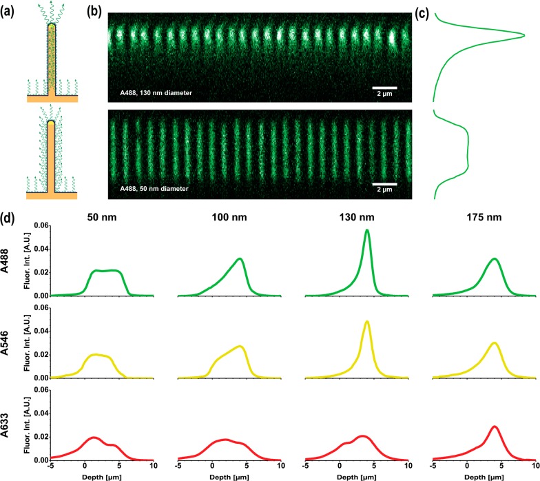
Lightguiding manifests itself in the fluorescence profiles as an increased emission intensity at the nanowire tips, compared to that observed along the nanowire length14 (Figure 2a,b). In order to assess the extent of lightguiding as a function of d and λ, we averaged the signal from all the nanowires in multiple fields of view (∼600 nanowires per typical 25 × 25 μm2 field of view, see Figure 2c), resulting in averaged intensity profiles along the nanowire length for each combination of d and λ (Figure 2d). Profiles of broken/fallen nanowires were excluded from the analysis, together with those of nanowires located within 0.5 μm from the image border, in order to avoid artifacts in the data analysis. To facilitate the comparison of the fluorescence profiles between nanowires of different sizes and/or labeled with different fluorophores, the profiles have been normalized to the area under the curve for visual comparison (see Supporting Information Section 4).
Figure 2.
(a) Schematic of the light emission pattern expected from lightguiding (top) and nonlightguiding (bottom) nanowires. (b) Confocal xz image (z-stack cross-section) of two A488-labeled nanowire arrays: 1 μm spacing, d = 130 nm (top) and d = 50 nm (bottom). The image of the thinner nanowires (bottom) shows homogeneous emission of light along the length of the nanowires, while the image of the thicker nanowires (top) shows emission increase at the nanowire tips, indicating that fluorescence emission couples into the nanowires and is guided to the tips. (c) Fluorescence intensity profiles obtained by averaging all nanowire profiles in the respective original images. (d) Representative fluorescence intensity profiles for nanowires of various d (left to right: 50, 100, 130, 175 nm) and with surface-attached fluorophores emitting at different wavelength ranges (see Supporting Information Section 3 for the emission spectra). Each profile shown is an average over several hundred nanowires. Profiles for all the tested d are available in Supporting Information Section 6. The profiles have been normalized to the area under the curve for visual comparison (details in Supporting Information Section 4).
We observe enhanced lightguiding properties, manifested by an intensity profile with a more pronounced peak near the nanowire tip, for larger d and for shorter λ (Figure 2d). Specifically, the thinnest nanowires (d = 50 nm) show a homogeneous fluorescence intensity profile along their length for all wavelengths, consistent with isotropic emission of fluorescence along the length of the wire. The observed slight increase in intensity near the substrate surface is attributed to the presence of fluorophores on the surface of the substrate between nanowires (see Supporting Information Section 5). In contrast, light emitted by fluorophores attached to nanowires of larger d appear to be coupled into the nanowire and guided to the nanowire tips (Figure 2a), in agreement with earlier reports.11,14 For a given d, the lightguiding effect increases as λ is decreased (Figure 2d, Supporting Information Section 6).
The observed dependence of the lightguiding effect on d and λ can be analyzed in analogy to step-index optical fibers. As the nanowire diameters are of the same order of magnitude as light wavelength in the visible range, coherent scattering/diffraction from different locations of the nanowire cross-section32 can lead to optical resonances that manifest as distinct optical modes in the nanowire. In the context of step-index optical fibers, the normalized frequency parameter, also referred to as V number,33 is frequently used to estimate the number of bound modes. V is defined as
| 1 |
where λ is the light wavelength, d is the diameter of the core of the fiber, and ncore and nclad are the refractive indexes of the core and the cladding of the fiber, respectively. In this case, we use the refractive index of water for the cladding, implicitly assuming the water cladding is extended infinitely and that there is no oxide coating. The approximation is justified as the refractive index of water (∼1.3) and alumina (∼1.7) are relatively similar, in contrast to the refractive index of gallium phosphide (∼3.4), and the alumina cladding is thin (10 nm).
To quantify the strength of the measured lightguiding effect (see Figure 3a), for a given combination
of d and λ, we determine the asymmetry of the
fluorescence signal along the nanowires, as illustrated in Figure 3b. For this purpose,
we define the asymmetry parameter  of
a fluorescence profile as the ratio
between the part toward the tip (t) and that toward
the base (b) of the full width calculated at 2/3
of the peak intensity value (Figure 3b). Based on this definition, a is
close to 0 for nonlightguiding nanowires (note that it is exactly
0 only for an ideal, infinitely long nanowire, while it is around
0.2 for a 3.5 μm long cylinder), and it is equal to 1 for ideal
lightguiding nanowires (see Supporting Information Section 7).
of
a fluorescence profile as the ratio
between the part toward the tip (t) and that toward
the base (b) of the full width calculated at 2/3
of the peak intensity value (Figure 3b). Based on this definition, a is
close to 0 for nonlightguiding nanowires (note that it is exactly
0 only for an ideal, infinitely long nanowire, while it is around
0.2 for a 3.5 μm long cylinder), and it is equal to 1 for ideal
lightguiding nanowires (see Supporting Information Section 7).
Figure 3.
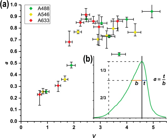
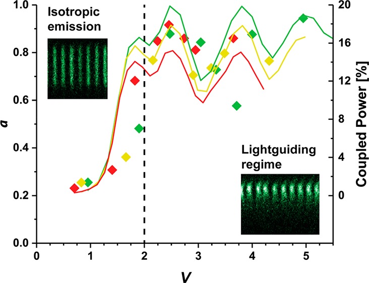
(a) Measured asymmetry parameter, a,
as a function
of the normalized frequency parameter, V, for every
combination of d and λ tested (color-coded
for wavelength as indicated in the legend). V was
calculated for each data point as a weighted average over the corresponding
fluorophore’s emission spectrum, resulting in the horizontal
error bars shown. Vertical error bars represent the deviation of a within the measurements. (b) Graphic representation of
how the asymmetry parameter  is defined (see main text for details;
axes are the same as those in Figure 2d). One expects a = 1 for a perfectly
symmetric peak, a = 0 for an infinitely long, nonlightguiding
nanowire, and a ≈ 0.2 for a nonlightguiding
wire about 3.5 μm long, observed under confocal illumination.
Examples of how the parameter a is determined are
given in the Supporting Information Section 7.
We find that the measured a value for the nanowires used in this study increases monotonically as a function of V for 0 < V < 2 and remains well above a = 0.5 for V > 2. This finding indicates that the lightguiding properties, as measured by a, are determined by the ratio between d and λ (since V is proportional to d/λ) and can be predicted by the value of V. For V > 2, the measured a value shows a considerable variance around a mean of about a ≈ 0.8.
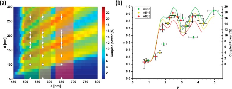
We have investigated this further by performing electromagnetic modeling based on the finite-difference time-domain (FDTD) approach, using Lumerical FDTD Solutions.34 In these simulations we have considered a single, infinitely long cylindrical GaP nanowire,35 coated with 10 nm of Al2O336 and surrounded by water. To simulate light emission from a single fluorophore, we have used an oscillating electric dipole point source located at 10 nm from the surface of the nanowire. To take into account the fact that fluorophores do not emit light at a fixed polarization we used an incoherent, unpolarized dipole (see Supporting Information Sections 8 and 9). The resulting electromagnetic field inside the nanowire was calculated as a function of time, and the coupling efficiency was determined by calculating the power transmitted along the nanowire at a distance of 3 μm from the emitting dipole, as a percentage of the total power emitted37,38 (Figure 4a). Note that the total in-coupled power in the nanowire is double the amount calculated this way: as the system is symmetric, an equal amount of power flows in the opposite direction along the nanowire, away from the dipole.
Figure 4.
Results from the FDTD simulations. (a) Predicted fraction of power coupled into an infinitely long nanowire for given d and λ. The plotted fraction refers to the power flow inside the nanowire at a location 3 μm from the emitting dipole, corresponding to half of the total power coupled into the nanowire (the other half flows in the opposite direction). The observed “ridges” in the coupled power are due to the contribution of different waveguide modes, white dots indicate the nanowire diameters used in the experiments, in correspondence to the peak emission wavelength for the three fluorophores. The three overlaid colored bands (green, yellow, and red) correspond to the emission ranges of the three tested fluorophores (A488, A546, and A633, emission spectra in Supporting Information Section 3). (b) Calculated coupling efficiency (colored solid lines) compared to the experimental data from Figure 3a (data points). As fluorophores emit over a range of wavelengths, the coupling efficiency was calculated, for each d, as an average of the results shown in (a) weighted over the fluorophores’ emission spectra.
The FDTD results, summarized in Figure 4a, show a series of ridges in the coupled power as a function of d and λ, consistent with the contribution of different waveguide modes, explaining the experimentally observed variance in lightguiding efficiency a for V > 2 (Figure 3a). This observation is consistent with previous work showing that higher order modes in nanowires can carry a significant fraction of power.23,39 Specifically, when plotting the calculated coupling efficiency as a function of V for the wavelength ranges used in the experiments, we find a variance in coupling efficiency, in good agreement with our experimental results (Figure 4b). Moreover, the step-like onset of lightguiding for V ≈ 2 observed in the experiments is consistent with the FDTD prediction. While the model used for Figure 4a considers an effectively infinitely long nanowire (see Supporting Information Section 8.1), we have checked that the in-coupling onset seen here is consistent with simulations that take finite-size effects into account (see Supporting Information Section 8.2).
Lightguiding in nanowires has previously often been discussed in terms of the fundamental HE11 waveguide mode, which gives lightguiding at the smallest diameter and which has been known to cause strong in-coupling of light in the form of absorption resonances.40,41 To gain understanding of the origin of the multiple ridges in Figure 4a, we analyzed in-coupling into all the waveguide modes that show up in the nanowire (see Supporting Information Section 10). The physical picture that emerges is that the fundamental HE11 mode describes the onset of lightguiding, as one can expect. However, for increasingly large d, the fundamental waveguide mode becomes too localized into the nanowire to allow efficient coupling into the wire. Then, emerging higher order modes take over the dominant role in lightguiding (see Supporting Information Section 10). This is because these higher-order, partially delocalized modes extend beyond the nanowire surface enough to overlap with fluorophores, but are sufficiently localized so as not to resemble a plane wave in the surrounding medium and to enable guiding in the nanowire.
By analyzing λ = 500 nm (see Supporting Information Section 10), we assign the first ridge at d ≈ 95 nm in Figure 4a to the fundamental HE11 mode, the second ridge at d ≈ 125 nm to the TE01 mode, the third ridge at d ≈ 180 nm to a combination of the HE21, TM01, and EH11 modes, the fourth ridge at d ≈ 250 nm to a combination of the HE12, HE31, and EH21 modes, and the next ridge at d > 300 nm appears to have contributions from the TM02 TE02, and HE41 modes.
In summary, we have established that the normalized frequency parameter, V, predicts the onset of fluorophore emission in-coupling in nanowires for V > 2 as a function of d and λ. Even though we find the threshold values of d and λ for lightguiding specifically for the material GaP in our experiments, our considerations are based on general optical principles and predict the same behavior more generally for any nonabsorbing material. Furthermore, we have shown that higher-order waveguide modes, beyond the fundamental HE11 mode, need to be taken into consideration to understand and predict the observed lightguiding behavior.
Lightguiding is expected to occur in any material with refractive index high enough to support waveguide modes at small d. However, it is important to also consider that materials with bandgaps smaller than the fluorophore emission wavelength will lead to losses caused by band-to-band absorption in the semiconductor, limiting the efficacy of the lightguiding effect for optical biosensing.
Besides the nanowire diameter and fluorophore emission wavelength considered here, the distance between fluorophores and surface of the III–V nanowire is another critical parameter for coupling. The role of this distance has, so far, only been investigated by changing the oxide coating thickness,15 which can alter the optical properties of a nanowire for thick coatings (>50 nm).42 Control over mode localization is also important and could be studied by using noncylindrical nanowires or by controlling tapering.43 Our analysis did not consider far-field diffraction in the microscope (i.e., confocal illumination and confocal detection) and near-field effects on the nanowire (fluorophore excitation, emission, and complete light–nanowire interaction), effects that should be included in a future model.
The presence of multimode lightguiding of light emitted from surface-bound fluorophores is important for biosensing, where the frequent use of several different fluorescent dyes in the same assay requires sensors that operate over a large wavelength interval. Based on our results, lightguiding can be predicted easily using the normalized frequency parameter V, without the need for numerical computation. The possibility to coat nanowires with various materials makes them versatile substrates for several surface chemistry approaches,9 and near-field effects (both for signal collection and in some cases enhanced illumination15) can be used for biosensing applications,11,15 enhancing the detection of fluorescence signals, for example, to detect the binding events between biomolecules and labeled ligands in solution.
Acknowledgments
We thank Dr. Steve Limpert for his help with the use of FDTD solutions. For financial support, we thank NanoLund, the Swedish Research Council (project number 2015-0612), the European Union’s Seventh Framework Programme (PhD4Energy, grant agreement no. 608153), the Horizon 2020 Research and Innovation Framework Programme of the European Union (Bio4Comp, grant agreement 732482, and NanoPokers, grant agreement no. 682206), and the Crafoord Foundation.
Supporting Information Available
The Supporting Information is available free of charge on the ACS Publications website at DOI: 10.1021/acs.nanolett.8b01360.
Details on nanowire fabrication, functionalization, imaging and data analysis, fluorophore emission spectra, fluorescence profile for all tested nanowire diameters, profile analysis, FDTD simulations, and analytical model on coupling into waveguide modes (PDF)
Author Present Address
∇ (A.P.D.) Pharmaceutical Sciences iMed Biotech Unit, AstraZeneca R&D Gothenburg, SE-431 83 Mölndal, Sweden.
Author Present Address
# (N.A.) Department of Electronics and Nanoengineering, Aalto University, P.O. Box 13500, FI-00076 Aalto, Finland.
The authors declare no competing financial interest.
Supplementary Material
References
- Anandan V.; Rao Y. L.; Zhang G. Nanopillar array structures for enhancing biosensing performance. Int. J. Nanomedicine 2006, 1, 73–79. 10.2147/nano.2006.1.1.73. [DOI] [PMC free article] [PubMed] [Google Scholar]
- Zhang G.-J.; Ning Y. Silicon nanowire biosensor and its applications in disease diagnostics: A review. Anal. Chim. Acta 2012, 749, 1–15. 10.1016/j.aca.2012.08.035. [DOI] [PubMed] [Google Scholar]
- Wang J. Carbon-nanotube based electrochemical biosensors: A review. Electroanalysis 2005, 17, 7–14. 10.1002/elan.200403113. [DOI] [Google Scholar]
- Gao Z.; et al. Silicon nanowire arrays for label-free detection of DNA. Anal. Chem. 2007, 79, 3291–3297. 10.1021/ac061808q. [DOI] [PubMed] [Google Scholar]
- Adalsteinsson V.; et al. Ultrasensitive Detection of Cytokines Enabled by Nanoscale ZnO Arrays. Anal. Chem. 2008, 80, 6594–6601. 10.1021/ac800747q. [DOI] [PubMed] [Google Scholar]
- Kim A.; et al. Ultrasensitive, label-free, and real-time immunodetection using silicon field-effect transistors. Appl. Phys. Lett. 2007, 91, 103901. 10.1063/1.2779965. [DOI] [Google Scholar]
- Chen K.-I.; Li B.-R.; Chen Y.-T. Silicon nanowire field-effect transistor-based biosensors for biomedical diagnosis and cellular recording investigation. Nano Today 2011, 6, 131–154. 10.1016/j.nantod.2011.02.001. [DOI] [Google Scholar]
- Hjort M.; et al. Electron microscopy imaging of proteins on gallium phosphide semiconductor nanowires. Nanoscale 2016, 8, 3936–3943. 10.1039/C5NR08888G. [DOI] [PubMed] [Google Scholar]
- Dabkowska A. P.; et al. Fluid and Highly Curved Model Membranes on Vertical Nanowire Arrays. Nano Lett. 2014, 14, 4286–4292. 10.1021/nl500926y. [DOI] [PubMed] [Google Scholar]
- Persson H.; Li Z.; Tegenfeldt J. O.; Oredsson S.; Prinz C. N. From immobilized cells to motile cells on a bed-of-nails: effects of vertical nanowire array density on cell behaviour. Sci. Rep. 2016, 5, 18535. 10.1038/srep18535. [DOI] [PMC free article] [PubMed] [Google Scholar]
- ten Siethoff L.; et al. Molecular Motor Propelled Filaments Reveal Light-Guiding in Nanowire Arrays for Enhanced Biosensing. Nano Lett. 2014, 14, 737–742. 10.1021/nl404032k. [DOI] [PMC free article] [PubMed] [Google Scholar]
- Warren-Smith S. C.; Afshar S.; Monro T. M. Fluorescence-based sensing with optical nanowires: a generalized model and experimental validation. Opt. Express 2010, 18, 9474–9485. 10.1364/OE.18.009474. [DOI] [PubMed] [Google Scholar]
- Linke H.; et al. Optical molecular nanowire sensor. European patent application 14178073.4, 2016.
- Frederiksen R. S.; et al. Modulation of Fluorescence Signals from Biomolecules along Nanowires Due to Interaction of Light with Oriented Nanostructures. Nano Lett. 2015, 15, 176–181. 10.1021/nl503344y. [DOI] [PubMed] [Google Scholar]
- Frederiksen R. S.; et al. Nanowire-Aperture Probe: Local Enhanced Fluorescence Detection for the Investigation of Live Cells at the Nanoscale. ACS Photonics 2016, 3, 1208–1216. 10.1021/acsphotonics.6b00126. [DOI] [Google Scholar]
- Johnson J. C.; et al. Single gallium nitride nanowire lasers. Nat. Mater. 2002, 1, 106–110. 10.1038/nmat728. [DOI] [PubMed] [Google Scholar]
- Law M.; et al. Nanoribbon Waveguides for Subwavelength Photonics Integration. Science 2004, 305, 1269. 10.1126/science.1100999. [DOI] [PubMed] [Google Scholar]
- Mayer B. Lasing from individual GaAs-AlGaAs core-shell nanowires up to room temperature. Nat. Commun. 2013, 4, 2931. 10.1038/ncomms3931. [DOI] [PubMed] [Google Scholar]
- Gudiksen M. S.; Lauhon L. J.; Wang J.; Smith D. C.; Lieber C. M. Growth of nanowire superlattice structures for nanoscale photonics and electronics. Nature 2002, 415, 617–620. 10.1038/415617a. [DOI] [PubMed] [Google Scholar]
- Wallentin J.; et al. InP Nanowire Array Solar Cells Achieving 13.8% Efficiency by Exceeding the Ray Optics Limit. Science 2013, 339, 1057. 10.1126/science.1230969. [DOI] [PubMed] [Google Scholar]
- Frederiksen R.; et al. Visual Understanding of Light Absorption and Waveguiding in Standing Nanowires with 3D Fluorescence Confocal Microscopy. ACS Photonics 2017, 4, 2235–2241. 10.1021/acsphotonics.7b00434. [DOI] [PMC free article] [PubMed] [Google Scholar]
- Duan X.; Huang Y.; Agarwal R.; Lieber C. M. Single-nanowire electrically driven lasers. Nature 2003, 421, 241. 10.1038/nature01353. [DOI] [PubMed] [Google Scholar]
- Voss T.; et al. High-Order Waveguide Modes in ZnO Nanowires. Nano Lett. 2007, 7, 3675–3680. 10.1021/nl071958w. [DOI] [PubMed] [Google Scholar]
- Johnson J. C.; Yan H.; Yang P.; Saykally R. J. Optical Cavity Effects in ZnO Nanowire Lasers and Waveguides. J. Phys. Chem. B 2003, 107, 8816–8828. 10.1021/jp034482n. [DOI] [Google Scholar]
- Zimmler M. A.; Capasso F.; Müller S.; Ronning C. Optically pumped nanowire lasers: invited review. Semicond. Sci. Technol. 2010, 25, 024001. 10.1088/0268-1242/25/2/024001. [DOI] [Google Scholar]
- Adolfsson K.; Schneider M.; Hammarin G.; Häcker U.; Prinz C. N. Ingestion of gallium phosphide nanowires has no adverse effect on Drosophila tissue function. Nanotechnology 2013, 24, 285101. 10.1088/0957-4484/24/28/285101. [DOI] [PubMed] [Google Scholar]
- Prinz C. N. Interactions between semiconductor nanowires and living cells. J. Phys.: Condens. Matter 2015, 27, 233103. 10.1088/0953-8984/27/23/233103. [DOI] [PubMed] [Google Scholar]
- Anttu N. Modifying the emission of light from a semiconductor nanowire array. J. Appl. Phys. 2016, 120, 043108. 10.1063/1.4960017. [DOI] [Google Scholar]
- Fukuzaki S.; Urano H.; Nagata K. Adsorption of bovine serum albumin onto metal oxide surfaces. J. Ferment. Bioeng. 1996, 81, 163–167. 10.1016/0922-338X(96)87596-9. [DOI] [Google Scholar]
- Urano H.; Fukuzaki S. Kinetic Study of Desorption of Two Species of Bovine Serum Albumin from Alumina during Alkali Elution Process. J. Colloid Interface Sci. 2002, 252, 284–289. 10.1006/jcis.2002.8500. [DOI] [PubMed] [Google Scholar]
- Schindelin J.; et al. Fiji: an open-source platform for biological-image analysis. Nat. Methods 2012, 9, 676–682. 10.1038/nmeth.2019. [DOI] [PMC free article] [PubMed] [Google Scholar]
- Anttu N. Geometrical optics, electrostatics, and nanophotonic resonances in absorbing nanowire arrays. Opt. Lett. 2013, 38, 730–732. 10.1364/OL.38.000730. [DOI] [PubMed] [Google Scholar]
- Bures J.Guided Optics: Optical fibers and all-fiber components; Wiley-VCH, 2008. [Google Scholar]
- Lumerical Solutions. FDTD Solutions; Lumerical Solutions, Inc., 2018. [Google Scholar]
- Aspnes D. E.; Studna A. A. Dielectric functions and optical parameters of Si, Ge, GaP, GaAs, GaSb, InP, InAs, and InSb from 1.5 to 6.0 eV. Phys. Rev. B: Condens. Matter Mater. Phys. 1983, 27, 985–1009. 10.1103/PhysRevB.27.985. [DOI] [Google Scholar]
- Malitson I. H. Refraction and Dispersion of Synthetic Sapphire. J. Opt. Soc. Am. 1962, 52, 1377–1379. 10.1364/JOSA.52.001377. [DOI] [Google Scholar]
- Paniagua-Dominguez R.; Grzela G.; Rivas J. G.; Sanchez-Gil J. A. Enhanced and directional emission of semiconductor nanowires tailored through leaky/guided modes. Nanoscale 2013, 5, 10582–10590. 10.1039/c3nr03001f. [DOI] [PubMed] [Google Scholar]
- Kivisaari P.; Chen Y.; Anttu N. Emission enhancement, light extraction and carrier dynamics in InGaAs/GaAs nanowire arrays. Nano Futur. 2018, 2, 015001. 10.1088/2399-1984/aaa666. [DOI] [Google Scholar]
- Maslov A. V.; Bakunov M. I.; Ning C. Z. Distribution of optical emission between guided modes and free space in a semiconductor nanowire. J. Appl. Phys. 2006, 99, 024314. 10.1063/1.2164538. [DOI] [Google Scholar]
- Anttu N.; Xu H. Q. Efficient light management in vertical nanowire arrays for photovoltaics. Opt. Express 2013, 21, A558–A575. 10.1364/OE.21.00A558. [DOI] [PubMed] [Google Scholar]
- Seo K.; et al. Multicolored Vertical Silicon Nanowires. Nano Lett. 2011, 11, 1851–1856. 10.1021/nl200201b. [DOI] [PubMed] [Google Scholar]
- Anttu N.; et al. Drastically increased absorption in vertical semiconductor nanowire arrays: A non-absorbing dielectric shell makes the difference. Nano Res. 2012, 5, 863–874. 10.1007/s12274-012-0270-x. [DOI] [Google Scholar]
- Bulgarini G.; et al. Nanowire Waveguides Launching Single Photons in a Gaussian Mode for Ideal Fiber Coupling. Nano Lett. 2014, 14, 4102–4106. 10.1021/nl501648f. [DOI] [PubMed] [Google Scholar]
Associated Data
This section collects any data citations, data availability statements, or supplementary materials included in this article.


