Abstract
This paper presents a single chip reduced-wire active catheter application-specific integrated circuit (ASIC), equipped with programmable transmit (Tx) beamforming and receive (Rx) time-division multiplexing(TDM).Theproposedfront-endASICis designed for driving a 64-channel one-dimensional transducer array in intracardiac echocardiography (ICE) ultrasound catheters. The ASIC is implemented in 60 V 0.18-μm HV-BCD technology, integrating Tx beam formers with high voltage pulsers and Rx front end in the same chip, which occupies 2.6 × 11 mm2 that can fit in the catheter size of 9 F (<3 mm). The proposed system reduces the number of wires from >64 to only 22 by integrating Tx beamformer that is programmable using a single low-voltage differential signaling data line. In Rx mode, the system uses 8:1 TDM with direct digital demultiplexing providing raw channel data that enables dynamic Rx beamforming using individual array elements. This system has been successfully used for B-mode imaging on standard ultrasound phantom with 401 mW of average power consumption. The ASIC has a compact element pitch-matched layout, which is also compatible with capacitive micromachined ultrasound transducer on CMOS application. This system addresses cable number and dimensional restrictions in catheters to enable ICE imaging under magnetic resonance imaging by reducing radio frequency induced heating.
Keywords: Capacitive micromachined ultrasound transducers (CMUT), intracardiac echocardiography (ICE), medical ultrasound imaging, time division multiplexing
I. Introduction
Intracardiac echocardiography (ICE) has become an important clinical modality in interventional ultrasound imaging [1], [2]. It requires a minimally invasive procedure with local anesthesia to place a catheter in the right side of the heart to guide interventions like valve repair, placement of stents, closure of atrial septal defects (ASD), and catheter- based ablation to treat atrial fibrillation [3].
Current commercial ICE catheters offer a 2D or limited 3D field of view in spite of large number of interconnections, which are mainly determined by the number of array elements and ground connections. Each element in the ICE array is connected to the analog-front-end (AFE) residing in an external ultrasound system with a separate long flexible wire, which is a significant limitation for improving image quality and increasing the number of elements. Also, in order to use ICE catheters under MRI instead of the ionizing X-ray radiation- based angiography, the number of interconnect wires in the catheter should be decreased to reduce RF-induced heating of the conducting lines to acceptable levels and the catheter tip should be visible [4], [5]. Reducing the number of connections by integrating electronics at the catheter tip would improve the overall system performance by capturing the receiver signals with higher fidelity, and transmitting them to the backend using higher quality cables which reduce the spurious interference present in the catheterization labs. Cable reduction would also improve the mechanical flexibility of these single use catheters, and possibly lower the cost. Therefore, integrating electronics at the catheter tip would have a significant impact in the catheter-based ultrasound imaging applications.
When designing the integrated systems on a chip for imaging application, ideally the quality of the resulting images should not be compromised while improving other aspects such as the cable count. In the application considered here, 64 element 2D imaging ICE catheter, to preserve the image quality, the raw data from each channel (without pre-combining signals from multiple array elements) should be available in the backend as in the current ICE catheters. That enables dynamic receive (Rx) beamforming techniques to be applied without limitations. The transmit (Tx) and Rx aperture size should be maximized making use of the full width of the catheter so that the image resolution and penetration depth are not compromised [6]. This requires Tx beamformer be integrated along with the Rx circuitry on the chip using a high voltage (HV) process and connected to the backend system with small number of cables and use the same maximum array area. Furthermore, the layout of the chip should be such that it is suitable for cable interconnect within the size limitations of the catheter tip. This paper demonstrates the first implementation of such an integrated system that combines a single cable programmable Tx beamformer and provides raw Rx data with 8:1 time division multiplexed receiver frontend for cable reduction.
On the Rx side, time division multiplexing (TDM) with direct digital demodulation (DDD) is used in this work as it provides −35 dB or below electrical crosstalk between channels with μ-coax cables suitable for ICE imaging [7]. This figure can be further reduced by digital signal processing techniques [8]. Noting that in current miniature ultrasound systems, electrical crosstalk below −25 dB is acceptable [9], TDM emerges as a viable and simple option as compared to more robust but more complex and power consuming digital data transmission. Frequency division multiplexing (FDM) also has been shown to be feasible to provide raw channel data for ICE application [10]. However, this approach requires multiple analog filters and mixers that are vulnerable to process variations, which will increase the mismatch and complexity of the system. Another common method to reduce the number of wires in ultrasound systems on the receiver side is subarray beamforming (μ-beamforming) [11].Recentimplementationsofthismethodincludeaswitchedcapacitor-based delay and addition of an on chip digitizer and digital line driver [12]. Another digital subarray beamformer uses ΔΣ modulator [13]. However, this system requires high frequency operation (960 MHz), which is difficult to feed into long interconnects in catheter-based applications, and limits integration of HV Tx circuits with thick gate oxide on a single chip. Note that these systems do not utilize the full aperture for Tx and Rx or do not integrate the Tx beamformer electronics which can be challenging to integrate with low voltage digital electronics. Furthermore, subarray beamforming methods inevitably compromise imaging performance as compared to a fully sampled array targeted here due to limited steering angles and angular directivity of the subarrays, which does not provide raw data information [14].
As mentioned above, the more critical aspect of cable reduction is single chip integration of the Tx beamformer at the catheter tip. Without Tx beamformer integration, only Rx cable reduction does not result in a practical imaging system. Single chip integration is essential to have a system size suitable for a catheter with a short rigid section at the tip. Single chip integration avoids complex through wafer vias for stacking chips and simplifies acoustic design. There are few examples of fully integrated Tx beamformer/Rx frontend systems. A system with more than 3000 transducer elements has been realized with Tx/Rx capability using subarray beamforming [15]. However, this system is developed for hand held probes to be used outside of the body. Other systems suitable in size for catheter implementation utilize subarray beamformers resulting in compromise in image quality and system complexity as noted by others [3], [12]. Other approaches to Tx beamformer implementation either require the number of cables proportional to the number of elements [16] with an external counter, or the beamformer has limited operation ability by only firing one pulse for each channel[17]‒[19]. Another on-chip beamformer with integrated counter was presented in [20], however, it still requires multiple control signals to generate pulse for each channel.
In this paper, we describe a single chip solution for 2D imaging ICE catheter system, which limits the ASIC design to 9 F (<3 mm width) in size, and less than 0.5 W of power as the main constraints. The proposed ASIC adopts 8:1 TDM with DDD and Tx beamforming circuit requiring a single low voltage differential signaling (LVDS) data line for cable reduction. This paper is organized as follows. Section II describes the proposed system architecture including brief explanation of backend system. The details of the Tx ASIC level operation is provided in Section III, and the Rx operation is described in Section IV. The electrical measurements and acoustic experiments are presented in Section V. Further discussion is presented in Section VI with comparison with the recent state-of-art before concluding in Section VII.
II. System Architecture
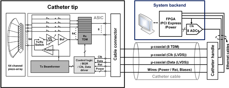
In a conventional ICE catheter system, each of the piezo-array elements at the catheter tip is connected to the AFE system of the mainframe using a long conducting line. To reduce the number of wires, the proposed system uses an ASIC at the catheter tip to implement the Tx beamformer and Rx TDM circuits in a single chip. Fig. 1 shows the simplified block diagram of the proposed ICE catheter system. Each 1D piezo- transducer array element is driven by a HV pulser, which can generate up to 60 V unipolar pulse, appropriately delayed based on the beamforming profile by the integrated beamformer. A Tx/Rx switch is located between pulser and Rx circuits to protect low voltage (LV) devices during Tx operation. Variable gain low noise amplifier (LNA) compensates for the attenuation of reflected echo signal by adjusting its gain to implement time gain compensation (TGC).
Fig. 1.
Simplified block diagram of the proposed ICE catheter system which includes backend system.
Eight sets of 8:1 TDM circuitry reduce the number of output signals from 64 to 8, and the high frequency (HF) buffers drive the TDM signals via Ethernet cables to the backend system. The ADC in the backend system samples the corresponding channel at the right time. A key feature of the TDM in this system is the clock synchronization between the external ADC and multiplexer in the ASIC, details of which will be described in the next section. In this system, 64 channels of piezo-array elements are used to interface with the ASIC in this proof-of-concept implementation. This array can be directly mounted on top of the front-end ASIC using flip-chip bonding or PZT-on-CMOS integration for future implementation [3], [12]. The proposed ASIC is also designed to be compatible with capacitive micromachined ultrasound transducer (CMUT)-on- CMOS application, where the array is fabricated directly over the CMOS wafer using a low temperature process [21].
The catheter cable consists of a mixture of μ-coax cables (200 MHz of clock, data, TDM output signals) and single wires to deliver power lines, biases and control signals. After the catheter cable, the TDM signals are amplified via catheter handle to be sent across the long Ethernet cables to ADCs in backend system, where DDD is performed in the FPGA for advanced imaging processing in the digital domain [7].
The backend system consists of a custom ADC board to support8TDMsignals,FPGAboard,andpowersupplymodule. It also employs filters, AC-DC converters, DC-DC converters, and a PCI express card, which delivers data from the FPGA to a personal computer via optical fiber.
III. Tx Beamformer and Pulser Design
A. Design and Operation of Tx Beamformer
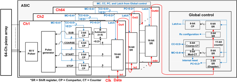
The proposed Tx beamformer uses a single LVDS data line to load the beamforming profile for 64 channels. It creates a maximum delay of 10.235 μs with a resolution of 5 ns, using an 11-bit global counter. This maximum delay enables steering the ultrasound beam over the desired ±45° field of view. The beamformer is designed to generate different pulse-width for each channel to control the Tx bandwidth and enable pulse-width apodization, which improves ultrasound image quality by suppressing the side lobe effects [22]. Also, it can generate multiple pulses up to 8, for narrow band higher SNR operation in pulsed Doppler mode. It also can change the pulse repetition frequency during Doppler mode operation.
Fig. 2 shows the detailed block diagram of Tx beamformer. In global control logic block, there is an 11-bit global counter that consists of 6-bit course counter (CC) and 5-bit mod counter (MC). During the data loading sequence, the initial value of 6bit CC is fixed to 1111112, and the counter starts counting down to 0000002 to find the coarse delay of each channel, while the 5-bit MC can be programmed to set the exact start time, width of a pulse, and number of pulses for each channel. Each of 64 channels has 16-bit serial-in parallel-out (SIPO) shift register that stores delay and pulse width information, respectively. Top 6-bit shift register is used to check proper data loading by comparing the value with 1111112. Once the data is loaded properly, the latch signal locks the shift registers and the counters start to count for pulse generation. A 2-bit shift register is used for Rx gain control configuration, and the last 3 bits of the shift register store the number of pulses for Doppler operation. Each channel has a 3-bit subtractor, which is used to keep track of how many pulses are fired during each transmitting cycle. Each channel has a 19-bit comparator that can calculate the exact beamforming profile to deliver LV pulses to the input of pulser.
Fig. 2.
Detailed block diagram of the Tx-beamformer.
To program the delay profile for all of the 64 channels, each programming cycle requires a 1040-bit data packet (64 × 16 + 2 +3 + 5 + 6), which corresponds to 5.2 μs. Before programming the Tx beamformer, all shift registers are reset to set initial values, following which the data packet is generated and sent from the FPGA in the backend system through the high speed Ethernet cables.
B. Design and Operation of HV Pulser
Ultrasound pulse generator, aka pulser, is one of the key building blocks of any ultrasound imaging system, which drives ultrasound transducers, such as piezoelectric transducer or CMUT with HV output swing to create a pressure pulse. Recent literature shows several pulse-level shifting techniques to overcome limited supply voltage such as voltage doubler or multi-level pulse generator in ultrasound application [23], [24]. However, these approaches require multiple control signals and occupy significant area, such that integrating them in the ICE catheter becomes challenging.
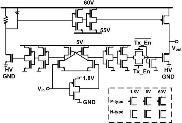
In this system, a digital pulser is implemented using 60 V double-diffused metal oxide semiconductor (DMOS) transistors, as shown in Fig. 3. The input of pulser is generated from Tx beamformer with 1.8 V supply. The pulser shifts this signal to 5 Vpp to have enough input swing for DMOS transistors, and finally drives the output node with 60 V pulse. It is crucial to ensure that all devices in the circuit are operated in their safe operating conditions throughout the pulse cycle, considering the fact that in this process, the drain-source junction breakdown and gate-oxide breakdown voltages are 60 V and 5 V, respectively. Considering that P-type DMOS transistor occupies larger area compared to the N-type DMOS transistor due to additional guard rings, a 1.3 kΩ resistor is used in level-shifter stage with protection Zener diode which has 5 V of breakdown voltage. This level shifter is designed to limit the peak current to 5 mA from 60 V supply by adding an external 55 V supply and 5 V buffer chain, avoiding voltage drop across 6.7 mm on-chip power routing. The pulser is designed to drive 15 pF of capacitive load at 7 MHz with 60 V pulses, which is the equivalent capacitance of comparably large sized piezoelectric 1D ICE array.
Fig. 3.
Schematic diagram of the proposed 60 V pulser.
IV. Rx Circuitry Design for Cable Reduction
Simplified schematic of the AFE is shown in Fig. 1. 64 channels of Rx circuitry consists of Tx/Rx switch, variable gain LNA, buffer and TDM circuitry. The LNA design assumes an input echo signal dynamic range of 76 dB, and the gain of Rx circuitry is set to compensate the attenuation by 4 stages (15 dB, 21 dB, 27 dB, and 32 dB) to meet the dynamic range of ADC in the backend system. During the Tx mode, Tx/Rx switch protects LV circuits from HV pulses. Variable gain LNA amplifies the echo signal based on the traveling depth for compensation, the buffer drives the amplified signal to TDM circuitry, and finally TDM circuitry samples and combines the output signals with 8:1 ratio to the backend system. The key blocks are described in detail below.
A. Design and Operation of Variable Gain LNA
Rx front-end topology in ultrasound system usually depends on the electrical impedance of ultrasound transducer type. The transimpedance amplifier (TIA) is a commonly used topology in CMUT application because the equivalent electrical model of CMUT has comparably high impedance [12]. For implementing the AFE for piezoelectric array, LNA structure is preferred because of relatively low impedance of piezoelectric elements [25]. Considering the area efficiency, and the fact that in this process capacitors occupy larger area than resistors, and for minimizing the shift of pulse-echo response to lower- frequencies, a resistive feedback LNA structure was selected for this system [26]. Also, instead of implementing LNA and time gain control (TGC) circuit separately, we adopted a variable gain LNA structure.
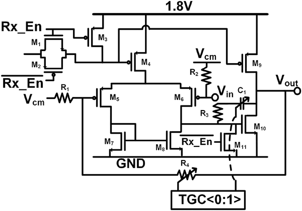
Fig. 4 shows the schematic diagram of variable gain LNA structure. The gain is controlled by 2-bit TGC control bits through data line, which is generated by the external FPGA. The Miller compensation capacitor, C1, is also controlled by TGC signal to push the second pole of this 2-stage op-amp well beyond the closed-loop bandwidth to keep phase margin above 60° in every gain stage of LNA. Rx_EN signal and switch transistors (M1, M2, and M11) are required for power saving mode during Tx data loading period.
Fig. 4.
Schematics of variable gain LNA.
B. Design and Operation of TDM Circuitry
The TDM technique has been frequently used in communication systems to reduce the number of outputs [27], [28]. This approach allows multiple channels to share the same cable by assigning a corresponding time slot to each channel. Analog TDM requires a relatively simple design and less power because it needs an analog multiplexer and digital counting logic in addition to sample and hold circuits, which is suitable for compact ICE application. Also in this proposed system, by using DDD technique, the ADC can sample TDM output signals using the same frequency as the TDM circuitry in the ASIC. This results in less data processing to increase efficiency in the backend system [7].
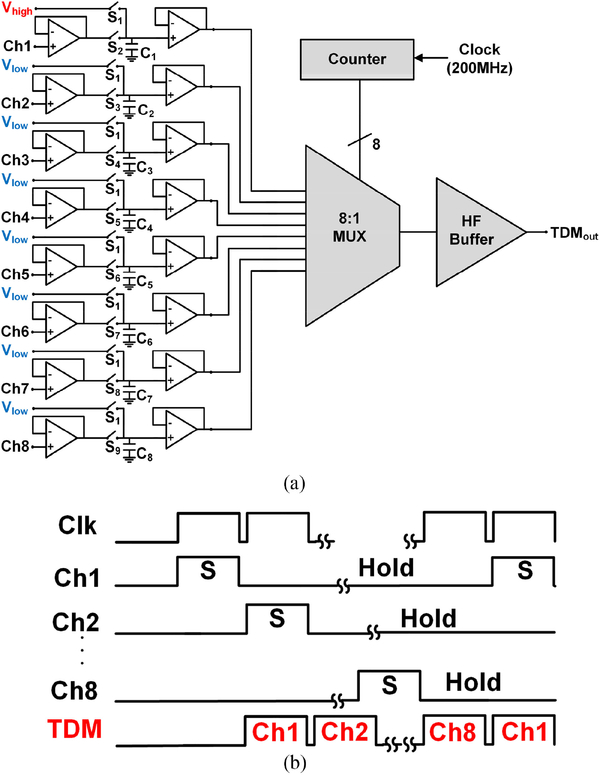
The Tx target center frequency of this system is around 7 MHz, and the 3 dB fractional bandwidth is assumed as 80%, especially in the case of CMUT array, which usually has broader bandwidth than a piezoelectric array. This bandwidth requires a sampling rate more than 20 MS/s considering the Nyquist requirement. In this system, the clock frequency is chosen as 200 MHz, resulting in 25 MS/s for each channel of 8:1 TDM circuitry. To minimize the TDM cross-talk level due to inter symbol interference, the HF buffer is designed to have more than 400 MHz bandwidth. The TDM circuitry consists of 8 sets of TDM blocks, and each TDM block consists of 8 channels of sample and hold switches, link training switches, analog 8:1 multiplexer, and high frequency buffer, as shown in Fig. 5(a). The TDM block is designed and placed symmetrically using H-grid clock distribution to reduce the mismatch. The counter logic generates sampling clocks and the analog multiplexer selects signals for corresponding channel after 1 period of clock, which keeps track of which channel is to be connected, as shown in Fig. 5(b).
Fig. 5.
(a) Simplified block diagram of TDM block for 8 channels. (b) TDM sampling clock diagram.
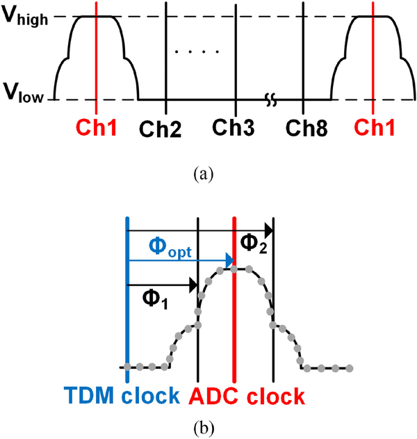
A critical part of the DDD is the clock synchronization between the TDM analog multiplexer in the ASIC and the ADC in the backend system with the same frequency. For this reason, the system requires two training sequences before TDM block starts working. One is channel number synchronization, and another is clock phase synchronization. These training sequences are called “link training” to ensure that the samples are correctly digitized in the backend system. During the link training process, first channel is connected to a fixed voltage level, Vhigh, while other channels are connected to another lower fixed voltage, Vlow, by adding another switch in parallel with the sample and hold switch for each channel, as shown in Fig. 5(a). During this operation, S1 is connected and all the other switches from S2 to S9 are open that the corresponding timing of channel 1 can be detected during demultiplexing in the backend system. By performing this step, the timing of the first channel of each TDM block can be ensured so that the order of channel timing is determined, as shown in Fig. 6(a).
Fig. 6.
Link training waveform of (a) channel number synchronization, and (b) phase synchronization.
The clock phase synchronization is used to ensure that the ADC and TDM multiplexer clocks are correctly phase synchronized to compensate for the propagation delays in the cabling. This is important as one needs to make sure that the ADC takes the samples when the signal through the interconnection has stabilized rather than during the switching transients. The TDM clock phase can be adjusted using a phase- locked loop (PLL) in the FPGA to determine the optimum phase shift, as shown in Fig. 6(b). The phase of TDM clock is changed with 78 ps steps until channel 1’s half maximum points are found, such as Φ1 and Φ2. These two points show when the switching transients are occurring, so optimal phase shift is estimated to be in the middle of these two points, which is marked as Φopt. The HF buffer is designed using current feedback source degenerated push-pull type buffers with ∼400 MHz bandwidth, tuned for 75 Ω cable termination [29].
V. Experimental Results
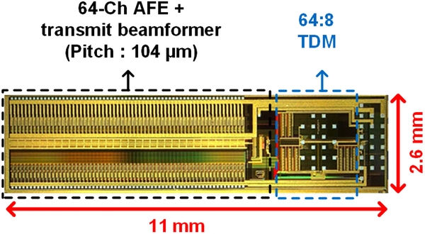
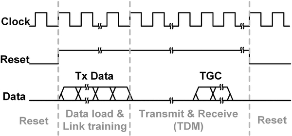
The ASIC is fabricated in a 0.18-μm 60 V power management 4M1P HV-BCD CMOS process. It consists of 64 channel AFE (pulser, Tx/Rx switch, LNA, and buffer), Tx beamformer, and symmetrically designed TDM, whichoccupies2.6×11mm2,as shown in Fig. 7. The pads for supplies, control signals and TDM outputs are located on the right side of ASIC, which are designed to be compatible with flip-chip interconnect based catheter cable connection. The chip consumes 401 mW of power on average for B-mode imaging using phased-array beamforming, 42% of which is used for TDM and drivers. Fig. 8 shows the timing diagram of the proposed system. The ASIC requires clock, reset, and data inputs. Once the Tx data is loaded properly after link training from the TDM side, the Tx beamformer triggers pulsers to fire HV pulses based on the beamforming profile, and Rx circuits are receiving at the same time. TGC signal can be loaded through data line to control the Rx gain at specific times. To eliminate the dead time during the Tx data loading, another set of Tx beamforming data can be loaded during receive period after Tx firing is done. After receiving the echo signals, reset signal returns the entire system back to the initial state. The link training always needs to be done before loading beamforming data, that compensates any change of the delay of the cable due to temperature change or bending.
Fig. 7.
Microphotograph of the 64-channel ICE ASIC, implemented in a 60 V, 0.18- μm HV-BCD CMOS process.
Fig. 8.
Timing diagram of the proposed system.
A. Electrical Characterization for Tx Circuitry
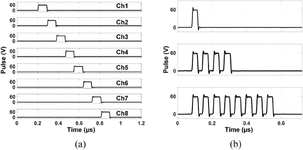
The ASIC was wire-bonded to a custom printed circuit board (PCB) to probe the output of the pulsers with the effective loading of ∼15 pF, which is the equivalent capacitance of 1D piezo-array with 80 membranes (each membrane occupies 46 × 46 μm2). The FPGA generates beamforming profile where each channel has the pulse width of 80 ns, and is delayed by 80 ns relative to the previous channel. Fig. 9(a) shows the measured pulse output from channel 1 to channel 8. The pulsers successfully generate 60 V pulses with rise and fall time of 6 ns, which is suitable for driving a center frequency of 7 MHz pulse. Fig. 9(b) shows that the proposed Tx beamformer can generate up to 8 pulses for Doppler operation.
Fig. 9.
(a) Measured pulser output from adjacent 8 channels. (b) Multiple consecutive pulse generation for Doppler imaging.
B. Electrical Characterization for LNA and Rx TDM
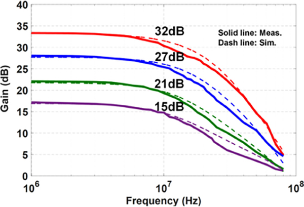
Fig. 10 compares the measured and simulated frequency response of variable gain LNA with different gain settings, which shows 15 dB, 21 dB, 27 dB, and 32 dB at center frequency of 7 MHz with 3 dB bandwidth of 11 MHz. The measured input referred noise at 7 MHz for different gain levels show less than 4.1 nV/Hz on average, close to the design target value of 5 nV/Hz, which is calculated from the assumed LNA input dynamic range.
Fig. 10.
Measured and simulated frequency response of variable gain LNA with different 4 gains.
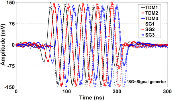
The proposed Rx TDM was separately characterized with a test chip to evaluate the performance of TDM circuitry. The test chip included a subset of blocks in the main ASIC, the ones needed to evaluate a block of 8 channels of TDM, as shown in Fig. 5(a), with an additional control block for link training. A custom PCB was designed to connect 8 input signals from external signal generators, and TDM output signal was connected to one of the backend TDM input terminals. The ADC samples the corresponding channel signals, then the FPGA performs DDD and further digital processing for interpolation, decimation, phase correction, and filtering to recover the original input data [7]. To test this signal chain, channel 1, 2, and 3 were connected to signal generators, which generated 7 MHz sine waves with 50 ns delay. Fig. 11 shows the comparison between digitized signal generator output and recovered TDM output signals after signal processing, which shows good agreement. The mismatch between the TDM outputs and signal generator outputs in the first and the last bursts is the result of band pass filtering. The mismatch between the channels is measured to be less than 0.6 dB in amplitude.
Fig. 11.
Comparison between the signal generator and TDM output signals after digital signal processing.
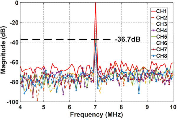
The level of crosstalk was also characterized in the TDM test chip. A 7 MHz sine wave was applied to channel 1, while inputs to other channels were grounded. The TDM signal was recovered for all 8 channels and analyzed using fast Fourier transform(FFT). Fig. 12 shows that the maximum cross talk level is −36.7 dB when compared to channel 1, which is suitable for ICE application [9]. It is noteworthy that this measurement of the crosstalk is between the signals of the same TDM block over the same cable as a result of the multiplexing scheme, which represent the worst case scenario. The crosstalk level between separate TDM blocks on different cables was measured to be below −60 dB.
Fig. 12.
Crosstalk measurement of 8 channels of TDM circuitry.
C. Ultrasound Imaging With the Entire System
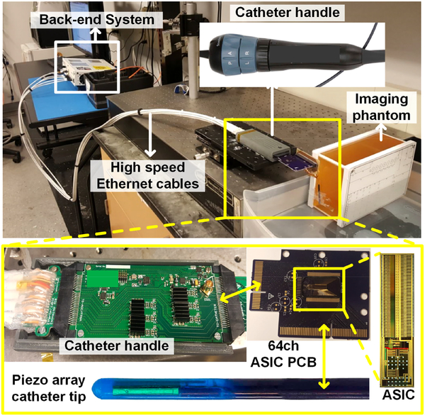
The proof-of-concept imaging experiments were performed by connecting the ASIC wire-bonded on a PCB, to a 64 channel piezoelectric transducer array at the tip of an ICE catheter using cables as shown in Fig. 13. The ASIC PCB is directly connected to catheter handle, which the TDM signals are amplified prior to passing through to the ADCs in the backend system via 3 m of Ethernet (Cat7A) cable to allow the system to be placed away from the MRI bore or the ultrasound mainframe in practice. In the future, the piezoelectric array will be either flip-chip bonded to the ASIC or the CMUT-on-CMOS technique will be applied for compact assembly, both of which are expected to reduce the parasitics and improve the resulting image.
Fig. 13.
Ultrasound imaging measurement setup with piezo-array immersed in the water facing standard phantom.
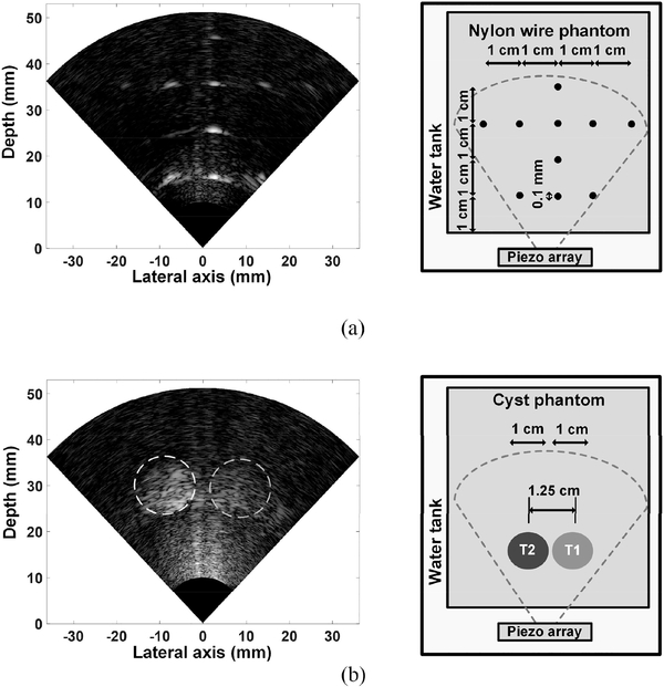
The piezoelectric transducer array is immersed in a water tank, facing a multi-purpose standardized tissue mimicking imaging phantom (N-365, Kyoto Kagaku, Japan). To form a cross-sectional B-scan image of the phantom, in Tx mode, the Tx beamformer is programmed to generate 123 focused and steered beams using suitable delay schemes to scan the ±45° sector image. In Rx mode, the echo signals captured by the ASIC front-end are transferred to the back-end system where the signals are post-processed and dynamic Rx beamforming is performed to reconstruct B-scan images [6]. Two different imaging targets inside the imaging phantom were used to test the performance of the system. First, a set of 10 nylon wire targets of 100 μm diameter were imaged. Fig. 14(a) shows the image of the 10 wire target, in which each wire is located 1 cm apart from others up to a depth ∼5 cm, as shown in the diagram on the right. The second target was 2 gray scale cyst phantoms at a depth of 3 cm, as shown in Fig. 14(b). Both images are presented with a dynamic range (DR) of 40 dB. The contrastto-noise-ratio (CNR) was also calculated for the cyst target to quantify the system performance. The CNR is defined as [30],
| (1) |
where μC and μB are the mean intensities of the regions inside the cyst and outside the cyst, respectively, and and are the corresponding variances. The CNR values for T1 and T2 cyst (Fig. 14(b)) were calculated as 1.55 and 1.23 with a relative contrast difference of 2 dB, which is in reasonable agreement with specs of the phantom [31].
Fig. 14.
(a) B-mode image of 10 nylon wires. (b) 2 cysts image in a standard phantom.
VI. Discussion
Overall, these results demonstrate the full functionality of the ASIC and backend system with a performance suitable for the targeted ICE application. Since the size of the pulser often limits the minimum size of Tx/Rx elements on the ASIC, the reduced capacitive loading with smaller 2D array elements will help to pitch-match the ASIC with a 2D ICE array implementation.
Table I benchmarks this work against the state-of-the-art ultrasound ASIC designs, where detailed information is available. As seen in the overall system comparison, this ASIC is the only system that integrates Tx/Rx without compromising imaging aperture and access to raw Rx data. This ASIC generates Tx delays from 5 ns to 10.235 μs to steer the ultrasound beam over the ±45° field of view, and has effectively 0 to 11 MHz pulse-echo system bandwidth. The die size is determined by the ICE application to fit in a 9 F catheter as shown in the ASIC micrograph (Fig. 7). Note that the power consumption per active chip area compares favorably with most other Rx cable reduction systems. AFE of each channel occupies 0.27 mm2, which is designed to match the pitch for future CMUT-on-CMOS design (element size: 2.6 × 0.104 mm2). Number of Rx cables is reduced by 8:1 TDM. Note that in case of a 2D array when TDM is used in conjunction with 3 × 3 subarray beamforming with switched-capacitor delay, this ratio can increase to 72:1.
Table I.
Benchmarking of the Reduced-Wire Ultrasound ASIC Systems
| Parameter | This work | [12] | [13] | [25] | [32] | [33] |
|---|---|---|---|---|---|---|
| Single chip integrated Tx-Rx system | Yes | No | No | No | No | No |
| Shared Tx-Rx array aperture with pitch match | Yes | No | N/A | No | No | No |
| Rx wire reduction | TDM | ADC + S/H analog | ADC + FIFO | S/H analog | Analog filter | S/H + Digital |
| Tx Wire reduction | Yes | No | No | No | No | No |
| Rx raw data accessibility | Yes | No | Yes | No | No | No |
| Center frequency (MHz) | 7 | 5 | 5 | 5 | 40 | 3 |
| Tx delay min (ns)/max(μs) | 5/10.235 | - | - | - | - | - |
| Die size (mm2) | 2.6×11 | 2.5×4.8 | 2.93×3.2 | 6.1×6.1 | 1.2×0.3 | 4.5×4.3 |
| Power/ Rx channel (mW) | 6.26 | 0.91 | 17.5 | 0.27 | 4.62 | 17.81 |
| Active area/ channel (mm2) | 0.27 | 0.026 | 0.088 | 0.026 | 0.045 | 0.303 |
| Power/ Rx active area (mW/ mm2) | 23.18 | 35 | 198.96 | 10.38 | 102.66 | 58.77 |
| # of channels | 64Tx/64Rx | 144Rx | 16Rx | 1024RX | 8Rx | 64Rx |
| # of wires / Rx channels | 8/64 | 4/144 | 1/16 | 96/1024 | 1/8 | 1/64 |
| # of wires/ Tx channels | 0.0625 (4/64) | 1 | 1 | 1 | 1 | 1 |
| Tx amplitude | 60V | - | - | - | - | - |
| Transducer | ID PZT/CMUT | 2DPZT | 2DCMUT | 2DPZT | Annular CMUT | 2D CMUT |
| Process | 0.18 μm HV | 0.18 μm | 28 nm | 0.18 μm | 0.35 μm | 0.13 μm |
The number of wires per Tx channel is reported as 4/64, including the data and clock wires, which is a significant advantage of this particular ASIC. It should be noted that this figure will further improve by increasing number of Tx channels for a system with larger number of elements as the required number of wires will remain the same. The size and power can be further optimized as the proposed ASIC is the first prototype for proof-of-concept for catheter-based ICE application, however even with non-ideal PCB based interconnect and partly operational PZT array, overall this novel system provides high dynamic range images of tissue mimicking phantoms.
VII. Conclusions
This work integrates both Tx beamformer and TDM based Rx in a single chip to reduce the number of interconnect wires in a 64 element 2D imaging ICE catheter. The Tx beamformer is capable of steering and focusing the Tx beams in a wide angular range and can be programmed in every firing using a single data line. The crosstalk levels and overall SNR of the resulting images indicate suitable performance for 2D imaging with 1D ICE arrays. The number of wires has been reduced from more than 64 down to 22 for this application, while maintaining full access to the raw data from each channel. More significant reduction is expected for 2D array-based systems with a larger number of elements. The reduction in cable count will not only create the potential for operation under MRI and reduce catheter cost, but it will also increase the mechanical flexibility and possibility of additional functionality in ICE catheters.
Acknowledgments
This work was supported by the National Institutes of Health under Grant HL121838. This paper was recommended by Associate Editor A. J.Burdett.
Biography
 Gwangrok Jung received the B.S. and M.S. degrees in electrical engineering from Seoul National University, Seoul, South Korea, in 2007 and 2009, respectively. He is currently working toward the Ph.D. degree in electrical and computer engineering at Georgia Institute of Technology, Atlanta, GA, USA. He was with the DMC R&D Center, Samsung Electronics, Suwon, South Korea, where he was involved in development of integrated circuits for portable ultrasound system. His research focuses on developing intracardiac echocardiography system with capacitive micromachined ultrasonic transducer and piezo transducer. His research interests include analog, digital, mixed-mode circuits design for biomedical applications, sensor interface IC, high-voltage circuit design, and system integration.
 Coskun Tekes (S’04–M’11) was born in Istanbul, Turkey, in 1976. He received the B.S. degree from Istanbul Technical University, Istanbul, Turkey, in 1998, and the M.S. and Ph.D. degrees from Isik University, Istanbul, Turkey, in 2002 and 2010, respectively, all in electrical and electronics engineering. Between 2004 and 2010, he was a Research Assistant with the Electronics Engineering Department, Isik University. Between 2010 and 2018, he was a Research Engineer with The George W. Woodruff School of Mechanical Engineering, Georgia Institute of Technology, Atlanta, GA, USA. He is currently an Assistant Professor with the School of Computer Engineering, Kennesaw State University, Marietta, GA, USA. His research interests include medical ultrasonic imaging and signal and image processing.
 M. Wasequr Rashid (S’10) received the B.Sc. degree in electrical and electronics engineering from the Bangladesh University of Engineering and Technology, Dhaka, Bangladesh, in 2004, the M.S. degree in electrical and computer engineering from New Mexico State University, Las Cruces, NM, USA, in 2010, and the Ph.D. degree in electrical and computer engineering from the Georgia Institute of Technology, Atlanta, GA, USA. He is currently working with Impinj Inc., Seattle, WA, USA.
 Thomas M. Carpenter received the M.Eng. degree in electronic and electrical engineering from the University of Leeds, Leeds, U.K., in 2014. He joined the Georgia Institute of Technology, Atlanta, GA, USA, as a Research Engineer developing high-speed field-programmable gate array designs for ultrasound imaging applications. He is currently a Visiting Researcher with the Ultrasound Research Group, University of Leeds. His current research interests include embedded systems and FPGA design, both in the biomedical field and for industrial applications.
 David Cowell (M’14) received the Ph.D. degree from the University of Leeds, Leeds, U.K., in 2008, for research on advanced coding techniques and excitation circuit design for industrial instrumentation and medical imaging ultrasound systems. He performed extensive consultancy in instrumentation, field-programmable gate arrays, and high-speed digital hardware design. Following work as a Research Consultant in measurement and instrumentation, he joined the Ultrasound Group, University of Leeds, as a Research Fellow. His current research interests include noninvasive industrial ultrasound measurement and advanced miniaturized ultrasound excitation systems with low harmonic distortion for phased array imaging, ultrasound system design, and signal processing.
 Steven Freear (S’95–M’97–SM’11) received the Doctorate degree in 1997. For seven years, he was a Medical Ultrasonic System Designer with the electronics industry. He was a Lecturer (Assistant Professor), Senior Lecturer (Associate Professor), and then Professor in 2006, 2008, and 2016, respectively, with the School of Electronic and Electrical Engineering, University of Leeds, Leeds, U.K. In 2006, he formed the Ultrasound Group, specializing in both industrial and biomedical research. He teaches digital signal processing, VLSI, and embedded systems design, and hardware description languages at both undergraduate and postgraduate levels. His main research interest includes advanced analog and digital signal processing and instrumentation for ultrasonic systems. He was elected as an Editor-in-Chief in 2013 for the IEEE TRANSACTION ON ULTRASONICS, FERROELECTRICS, AND FREQUENCY CONTROL. In June 2014, he was appointed as a Visiting Professor with Georgia Tech, Atlanta, GA, USA. He is an External Examiner for undergraduate programmes in electronic engineering with Queen’s University, Belfast, U.K.
 F. Levent Degertekin received the B.S. degree from Middle East Technical University, Ankara, Turkey, in 1989, the M.S. degree from Bilkent University, Ankara, Turkey, in 1991, and the Ph.D. degree from Stanford University, Stanford, CA, USA, in 1997, all in electrical engineering. During 1992–1993 academic year, he was a Visiting Scholar with the E.L. Ginzton Laboratory, Stanford University, where he was also an Engineering Research Associate from 1997 to 2000. He is currently the G.W. Woodruff Chair in mechanical systems, and a Professor with The G.W. Woodruff School of Mechanical Engineering and the School of Electrical and Computer Engineering, Georgia Institute of Technology, Atlanta, GA, USA. He has authored and coauthored more than 50 U.S. patents and 100 journal publications. His research interests include micromachined acoustic and opto-acoustic devices, medical ultrasound imaging bioanalytical instrumentation, and atomic force microscopy. He was an Associate Editor for the IEEE SENSORS JOURNAL and is currently an Associate Editor for the IEEE TRANSACTIONS ON ULTRASONICS, FERROELECTRICS AND FREQUENCY CONTROL. He also serves on the Technical Program Committee of the IEEE International Ultrasonics Symposium. He was the recipient of the NSF CAREER award for his work on ultrasonic atomic force microscopy in 2004, the IEEE Ultrasonics, Ferroelectrics, and Frequency Control Society 2004 Outstanding Paper award, with his students, and most recently the IEEE UFFC Society 2014 Carl Hellmuth Hertz Ultrasonic Achievement Award.
 Maysam Ghovanloo (S’00–M’04–SM’10) received the B.S. degree in electrical engineering from the University of Tehran, Tehran, Iran, the M.S. degree in biomedical engineering from the Amirkabir University of Technology, Tehran, Iran, in 1997, and the M.S. and Ph.D. degrees in electrical engineering from the University of Michigan, Ann Arbor, MI, USA, in 2003 and 2004.
From 2004 to 2007 he was an Assistant Professor with the Department of ECE, North Carolina State University, Raleigh, NC, USA. Since 2007 he has been with the School of Electrical and Computer Engineering, Georgia Institute of Technology, Atlanta, GA, USA, where he is currently a Professor and the Founding Director with the GT-Bionics Lab. He has 5 issued patents and authored or coauthored more than 200 peer-reviewed conferences and journal publications on implantable microelectronic devices, integrated circuits and micro-systems for IMD applications, and modern assistive technologies.
Dr. Ghovanloo is currently an Associate Editor for the IEEE TRANSACTIONS ON BIOMEDICAL ENGINEERING and IEEE TRANSACTIONS ON BIOMEDICAL CIRCUITS AND SYSTEMS. He was the General Chair for the IEEE BIOMEDICAL CIRCUITS AND SYSTEMS (BioCAS 2015) in Atlanta, GA, USA, in Oct. 2015. He served as an Associate Editor for the IEEE TRANSACTIONS ON CIRCUITS AND SYSTEMS, PART II (2008–2011) and a Guest Editor for the IEEE JOURNAL OF SOLID-STATE CIRCUITS and IEEE TRANSACTIONS ON NEURAL SYSTEMS AND REHABILITATION ENGINEERING. He was the recipient of the National Science Foundation CAREER Award, the Tommy Nobis Barrier Breaker Award for Innovation, and Distinguished Young Scholar Award from the Association of Professors and Scholars of Iranian Heritage.
Contributor Information
Gwangrok Jung, School of Electrical and Computer Engineering, Georgia Institute of Technology, Atlanta, GA 30308 USA (grjung84@gmail.com).
Coskun Tekes, School of Computer Engineering, Kennesaw State University, Marietta, GA 30060 USA (ctekes@kennesaw.edu).
M. Wasequr Rashid, Impinj Inc., Seattle, WA 98109 USA (waseq117@gmail.com).
Thomas M. Carpenter, School of Electronic and Electrical Engineering, University of Leeds, Leeds LS2 9JT, U.K. (T.Carpenter@leeds.ac.uk)
David Cowell, School of Electronic and Electrical Engineering, University of Leeds, Leeds LS2 9JT, U.K. (D.M.J.Cowell@leeds.ac.uk).
Steven Freear, School of Electronic and Electrical Engineering, University of Leeds, Leeds LS2 9JT, U.K. s.freear@leeds.ac.uk.
F. Levent Degertekin, School of Electrical and Computer Engineering, Georgia Institute of Technology, Atlanta, GA 30308 USA, and also with the School of Mechanical Engineering, Georgia Institute of Technology, Atlanta, GA 30332 USA.
Maysam Ghovanloo, School of Electrical and Computer Engineering, Georgia Institute of Technology, Atlanta, GA 30308 USA.
References
- [1].Saliba W and Thomas J, “Intracardiac echocardiography during catheter ablation of atrial fibrillation,” Europace, vol. 10, no. suppl 3, pp. 42–47, 2008. [DOI] [PubMed] [Google Scholar]
- [2].Kim SS, Hijazi ZM, Lang RM, and Knight BP, “The use of intracardiac echocardiography and other intracardiac imaging tools to guide noncoronary cardiac interventions,” J. Amer. College Cardiology, vol. 53, no. 23, pp. 2117–2128, 2009. [DOI] [PubMed] [Google Scholar]
- [3].Wildes D et al. , “4-D ICE: A 2-D array transducer with integrated ASIC in a 10-Fr catheter for real-time 3-D intracardiac echocardiography,” IEEE Trans. Ultrason., Ferroelect., Freq. Control, vol. 63, no. 12, pp. 2159–2173, Dec. 2016. [DOI] [PubMed] [Google Scholar]
- [4].Dempsey MF, Condon B, and Hadley DM, “Investigation of the factors responsible for burns during MRI,” J. Magn. Reson. Imag, vol. 13, no. 4, pp. 627–631, 2001. [DOI] [PubMed] [Google Scholar]
- [5].Mirbozorgi SA et al. , “A feasibility study for MRI guided CMUT-based intracardiac echocardiography catheters,” in Proc. IEEE Int. Ultrason. Symp., 2017, pp. 1–4. [Google Scholar]
- [6].Szabo TL, Diagnostic Ultrasound Imaging: Inside Out, 2nd Ed. Boston, MA, USA: Academic Press, 2014. pp. 209–250. [Google Scholar]
- [7].Carpenter TM, Rashid MW, Ghovanloo M, Cowell DMJ, Freear S, and Degertekin FL, “Direct digital demultiplexing of analog TDM signals for cable reduction in ultrasound imaging catheters,” IEEE Trans. Ultrason., Ferroelect., Freq. Control, vol. 63, no. 8, pp. 1078–1085, Aug. 2016. [DOI] [PMC free article] [PubMed] [Google Scholar]
- [8].Liu Q, Chen C, Chang Z, Prins C, and Pertijs MAP, “A mixed-signal multiplexing system for cable-count reduction in ultrasound probes,” in Proc. IEEE Int. Ultrason. Symp., 2015, pp. 1–4. [Google Scholar]
- [9].Oakley C, Mueller J, Dietz D, and Kuhnke J, “A minimally invasive ultrasound probe using non-coax cabling,” in Proc. IEEE Int. Ultrason. Symp, Oct. 2001, vol. 2, pp. 1011–1016. [Google Scholar]
- [10].Rashid MW, Tekes C, Ghovanloo M, and Degertekin FL, “Design of frequency-division multiplexing front-end receiver electronics for CMUTon-CMOS based intracardiac echocardiography,” in Proc. IEEE Int. Ultrason. Symp., Sep. 2014, pp. 1540–1543. [Google Scholar]
- [11].Savord B and Solomon R, “Fully sampled matrix transducer for real time 3D ultrasonic imaging,” in Proc. IEEE Int. Ultrason. Symp, 2003, vol. 1, pp. 945–953. [Google Scholar]
- [12].Chen C et al. , “A pitch-matched front-end ASIC with integrated subarray beamforming ADC for miniature 3-D ultrasound probes,” IEEE J. Solid-State Circuits, vol. 53, no. 11, pp. 3050–3064, Nov. 2018. [Google Scholar]
- [13].Chen MC et al. , “A pixel-pitch-matched ultrasound receiver for 3D photoacoustic imaging with integrated delta-sigma beamformer in 28 nm UTBB FDSOI,” in Proc. IEEE Int. Solid-State Circuits Conf., Feb. 2017, pp. 456–457. [DOI] [PMC free article] [PubMed] [Google Scholar]
- [14].Santos P, Haugen GU, Løvstakken L, Samset E, and D’hooge J, “Diverging wave volumetric imaging using subaperture beamforming,” IEEE Trans. Ultrason., Ferroelect., Freq. Control, vol. 63, no. 12, pp. 2114–2124, Dec. 2016. [DOI] [PubMed] [Google Scholar]
- [15].Katsube Y et al. , “Single-chip 3072ch 2D array IC with RX analog and all-digital TX beamformer for 3D ultrasound imaging,” in Proc. IEEE Int. Solid-State Circuits Conf., Feb. 2017, pp. 458–459. [Google Scholar]
- [16].Chen K, Lee HS, and Sodini CG, “A column-row-parallel ASIC architecture for 3-D portable medical ultrasonic imaging,” IEEE J. SolidState Circuits, vol. 51, no. 3, pp. 738–751, Mar. 2016. [Google Scholar]
- [17].Bhuyan A et al. , “3D volumetric ultrasound imaging with a 32 × 32 CMUT array integrated with front-end ICs using flip-chip bonding technology,” in Proc. IEEE Int. Solid-State Circuits Conf., Feb. 2013, pp. 396–397. [Google Scholar]
- [18].Bhuyan A et al. , “Integrated circuits for volumetric ultrasound imaging with 2-D CMUT arrays,” IEEE Trans. Biomed. Circuits Syst, vol. 7, no. 6, pp. 796–804, Dec. 2013. [DOI] [PubMed] [Google Scholar]
- [19].Rashid MW et al. , “Front-end electronics for cable reduction in intracardiac echocardiography (ICE) catheters,” in Proc. IEEE Int. Ultrason. Symp., Sep. 2016, pp. 1–4. [Google Scholar]
- [20].Jung SJ, Song JK, and Kwon OK, “Three-side buttable integrated ultrasound chip with a 16 × 16 reconfigurable transceiver and capacitive micromachined ultrasonic transducer array for 3-D ultrasound imaging systems,” IEEE Trans. Electron Devices, vol. 60, no. 10, pp. 3562–3569, Oct. 2013. [Google Scholar]
- [21].Gurun G, Hasler P, and Degertekin FL, “Front-end receiver electronics for high-frequency monolithic CMUT-on-CMOS imaging arrays,” IEEE Trans. Ultrason. Ferroelect., Freq. Control, vol. 58, no. 8, pp. 1658–1668, Aug. 2011. [DOI] [PMC free article] [PubMed] [Google Scholar]
- [22].Smith PR, Cowell DMJ, and Freear S, “Width-modulated square-wave pulses for ultrasound applications,” IEEE Trans. Ultrason., Ferro-elect., Freq. Control, vol. 60, no. 11, pp. 2244–2256, Nov. 2013. [DOI] [PubMed] [Google Scholar]
- [23].Jung G, Tekes C, Pirouz A, Degertekin L, and Ghovanloo M, “Supplydoubledpulse-shapinghighvoltagepulserforCMUTarrays,”IEEETrans. Circuits Syst. II, Express Briefs, vol. 65, no. 3, pp. 306–310, Mar. 2018. [DOI] [PMC free article] [PubMed] [Google Scholar]
- [24].Chen K, Lee H-S, Chandrakasan AP, and Sodini CG, “Ultrasonic imaging transceiver design for CMUT: A three-level 30-Vpp pulse-shaping pulser with improved efficiency and a noise-optimized receiver,” IEEE J. Solid-State Circuits, vol. 48, no. 11, pp. 2734–2745, Nov. 2013. [Google Scholar]
- [25].Chen C et al. , “A front-end ASIC with receive sub-array beamforming integrated with a 32 × 32 PZT matrix transducer for 3-d transesophageal echocardiography,” IEEE J. Solid-State Circuits, vol. 52, no. 4, pp. 994–1006, Apr. 2017. [Google Scholar]
- [26].Sautto M, Savoia AS, Quaglia F, Caliano G, and Mazzanti A, “A comparative analysis of CMUT receiving architectures for design optimization of integrated transceiver front-ends,” IEEE Trans. Ultrason., Ferroelect., Freq. Control, vol. 64, no. 5, pp. 826–838, Feb. 2017. [DOI] [PubMed] [Google Scholar]
- [27].Stern HPE and Mahmoud SA, Communication Systems: Analysis and Design. Englewood Cliffs, NJ, USA: Prentice Hall, 2004. [Google Scholar]
- [28].Spirit D, Ellis AD, and Barnsley P, “Optical time division multiplexing: Systems and networks,” IEEE Commun. Mag, vol. 32, no. 12, pp. 56–62, Dec. 1994. [Google Scholar]
- [29].Manetakis K, Toumazou C, Papavassiliou C, “A 120 MHz, 12 mW CMOS current feedback opamp,” in Proc. IEEE Custom Integr. Circuits Conf, May 1998, pp. 365–368. [Google Scholar]
- [30].Karaman M, Li PC, and O’Donnell M, “Synthetic aperture imaging for small scale systems,” IEEE Trans. Ultrason., Ferroelect., Freq. Control, vol. 42, no. 3, pp. 429–442, May 1995. [Google Scholar]
- [31].Kyoto Kagaku America Inc., “US-2: N-365 multipurpose QA phantom.” [Online]. Available: https://www.kkamerica-inc.com/us-2_n-365_multipurpose_qa_phantom. Accessed on: Jul. 18, 2018.
- [32].Gurun G, Zahorian JS, Sisman A, Karaman M, Hasler PE, and Degertekin FL, “An analog integrated circuit beamformer for high-frequency medical ultrasound imaging,” IEEE Trans. Biomed. Circuits Syst, vol. 6, no. 5, pp. 454–467, Oct. 2012. [DOI] [PubMed] [Google Scholar]
- [33].Um JY et al. , “An analog-digital-hybrid single-chip Rx beamformer with non-uniform sampling for 2D-CMUT ultrasound imaging to achieve wide dynamic range of delay and small chip area,” in Proc. IEEE Int. Solid-State Circuits Conf. Dig. Tech. Papers, Feb. 2014, pp. 426–427. [Google Scholar]


