Abstract
This paper presents a fully integrated photodiode-based low-power and low-mismatch stimulator for a subretinal prosthesis. It is known that a subretinal prosthesis achieves 1600-pixel stimulators on a limited single-chip area that is implanted beneath the bipolar cell layer. However, the high-density pixels cause high power dissipation during stimulation and high fabrication costs because of special process technologies such as the complementary metal-oxide semiconductor CMOS image sensor process. In addition, the many residual charges arising from the high-density pixel stimulation have deleterious effects, such as tissue damage and electrode corrosion, on the retina tissue. In this work, we adopted a switched-capacitor current mirror technique for the single-pixel stimulator (SPStim) that enables low power consumption and low mismatch in the subretinal device. The customized P+/N-well photodiode used to sense the incident light in the SPStim also reduces the fabrication cost. The 64-pixel stimulators are fabricated in a standard 0.35-μm CMOS process along with a global digital controller, which occupies a chip area of 4.3 × 3.2 mm2 and are ex-vivo demonstrated using a dissected pig eyeball. According to measured results, the SPStim accomplishes a maximum biphasic pulse amplitude of 143 μA, which dissipates an average power of 167 μW in a stimulation period of 5 ms, and an average mismatch of 1.12 % between the cathodic and anodic pulses.
Keywords: subretinal prosthesis, photodiode, high-density pixels, ex-vivo demonstration, light sensor, digital controller, implantable device
1. Introduction
Retinal implants offer great promise for restoring vision to patients who suffer from retinal diseases such as retina pigmentosa and age-related macular degeneration. According to the anatomical position, retinal prostheses can be classified as epiretinal [1,2], subretinal [3,4,5], or suprachoroidal [6,7] devices. Among them, it has been reported that the subretinal implant can provide high pixel density of up to 1600 pixels [8], on a limited silicon chip area [9]; this is possible because the stimulator in the subretinal device does not need a high-resolution current-steering digital-to-analog converter (DAC) and its own local digital controller, which are employed to generate various biphasic current pulses for epiretinal and suprachoroidal prosthetics. The high-resolution DAC and the digital controller occupy a large area in a single-pixel stimulator (SPStim); the area becomes dominant with high-voltage CMOS (complementary metal-oxide semiconductor) process technology [2].
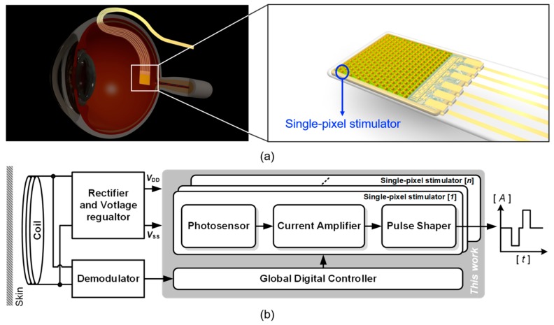
Figure 1a shows a subretinal prosthesis that is inserted into the subretinal space of the eye via ab-externo approach. The prosthetic chip and cable, which works to deliver a power and a command data from an inductive coupling coil located in the retroauricular area, enters the subretinal space passing through the partial-thickness scleral flap. Then, the rest cable outside the eye is buried under the temporalis muscle. Figure 1b depicts the general architecture of a single-pixel stimulator (SPStim) for a subretinal implant, which is composed of a photosensor, a current amplifier, and a pulse shaper. A photodiode in the photosensor produces a dark current corresponding to the light intensity incoming onto the retina. The dark current is in the order of nano-amperes and has a monophasic shape. The current amplifier in Figure 1b works to amplify the dark current from tens to hundreds of microamperes. Finally, the pulse shaper reshapes the amplified monophasic signal to a biphasic current pulse, which consists of a rectangular cathodic and anodic pulse, and then delivers the biphasic signal into the bipolar cells interfaced with a microelectrode.
Figure 1.
(a) System overview of a subretinal prosthesis that is implanted beneath the bipolar cell layer, (b) simplified architecture of the subretinal device including the single-pixel stimulator.
The single-pixel stimulator for the subretinal prosthesis should meet three design requirements as follows. First, the amplitude mismatch of the cathodic and anodic pulses should be as low as possible in order to reduce the residual charge on the retina tissue after stimulation. The residual charge sometimes induces unwanted spike excitation that results in tissue damage, as well as electrode corrosion that impedes the delivery of stimulation charge to the tissue from the stimulator output [10]. Thus, it is indispensable to minimize the amplitude mismatch of the biphasic stimulus current. Second, it must be fully controllable by digital logic embedded on the same chip in order to generate the diverse shapes of the biphasic stimulus current. Because visually impaired patients have individually different thresholds for exciting the nerves in the retina [11], after implantation, the stimulus current shapes must be adjusted, including the amplitude, width, period of the biphasic stimuli, and the interphase delay between the cathodic and anodic pulses. Finally, the stimulator necessitates a wide dynamic output range to produce various amplitudes of the biphasic current owing to the different thresholds of the patients to excite their retinal nerves. A simple way to widen the output dynamics is to raise the power supply rail. However, the high-voltage operation leads to high power consumption in the SPStim, which would become worse in a subretinal device with high-density pixels. We thus must devise a new SPStim architecture to accomplish the wide dynamic output range while maintaining low-voltage operation.
Over the last decade, a few single-pixel stimulators have been presented for subretinal implants to implement high-density stimulator arrays [3], low-voltage operation [12], and low mismatch [6,13]. To the authors’ best knowledge, however, any results that meet all of these design requirements have not yet been presented. Thus motivated, in this work we propose a SPStim design that adopts a switched-capacitor current mirror technique that achieves both low mismatch and wide dynamic output range in low-voltage operation. This stimulator circuit was fabricated in a standard 0.35-μm 4M2P CMOS process and ex-vivo demonstrated employing a dissected pig eyeball.
2. Methods
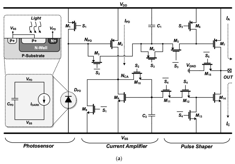
Figure 2 shows the circuit diagram of the proposed SPStim, which is composed of three stages: (1) a photosensor, (2) a current amplifier, and (3) a pulse shaper, as illustrated in Figure 1b. Also shown are simulated transient waveforms for the SPStim’s digital inputs and analog output. The photosensor stage is composed of a photodiode DPD and a PMOS transistor M1, which works as a switch to reset DPD. In this design, a customized photodiode that has the structure of a P+ and N-well as illustrated in Figure 2a has been employed because of its high sensitivity [14] and relatively low fabrication cost compared with the CMOS image sensor process that requires a deeper epitaxial layer, anti-reflective coating and optimization of passivation in order to minimize interference [15]. DPD can be modeled as a dark current source IDARK, which is proportional to the incident light intensity, and a parasitic capacitor CPD, which arises from the junction area of the P+ and N-well in the diode, Cgd1, Cgs3, Cgs2, and Cgs2. Here, Cgd, and Cgs denote a gate-drain and gate-source parasitic capacitance of the transistors. Although IDARK and CPD respectively vary with the light intensity and the dimension of DPD and its adjacent transistors, we set IDARK and CPD to 8 nA and 6 pF for the simulation environment.
Figure 2.
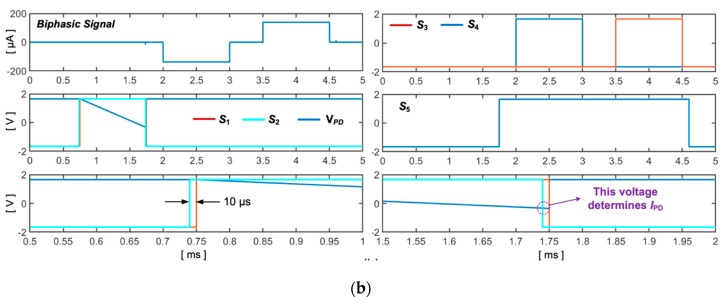
(a) Circuit diagram of the proposed single-pixel stimulator adopting a customized photodiode and a switched capacitor current mirror technique; (b) simulated transient waveform to show input and analog output.
The proposed SPStim operates in four different modes: the preset mode (0–0.74 ms in Figure 2b), reset mode (0.74–0.75 ms), charging mode (0.75–1.75 ms), and stimulation mode (0.175–4.6 ms), followed by the next preset mode (0.46–5 ms). During the preset mode, where all signals of the digital controller are set to logic 0, the PMOS transistor M1 is fully turned on, and as a result, CPD is charged up to VDD. The stages other than the photodiode stage are deactivated in this mode to diminish unnecessary power dissipation. By applying a logic 1 to the S2 on M3 and M10 in the current amplifier stage, the reset mode begins, where the capacitors C1 and C2 are reset to VDD through M1 and M3, and to VSS through M8 and M10, respectively. Thus, the previous stimulation memory recorded on C1 and C2 is erased so as to receive new stimulation information.
The charging mode starts when the S1 on M1 and M8 becomes logic 1. The S1 is synchronized with the S2, but its rising and falling edges lag those of the S2 by 10 μs. We generate the S1 from the S2 using a simple delay chain as presented in [16]. As the S1 turns high, the transistor M1 is immediately disabled. Because of the IDARK, the node voltage of NPD, here called VPD, begins to steadily drop from VDD to VDD − IDARK × ΔT/(C1 + CPD), where ΔT indicates the duration of the charging mode (0.75–1.75 ms in this simulation). The drop in VPD enables the PMOS transistor M2, thereby entering it to a saturation region. Accordingly, the current IPD generated from M2 can be defined as
| (1) |
Here, μP, COX, W/L, and VTH,P are the channel mobility, gate oxide capacitance per unit area, aspect ratio, and PMOS threshold voltage, respectively. This equation shows that the small current IDARK in the nano-ampere range is amplified to a stimulus current in the tens to hundreds of micro-amperes by adjusting the charging duration ΔT. In this work, we aimed to generate a stimulation current of 150 μA at maximum. Because IPD produced from M2 flows out to VSS only through M9, IPD can be transformed to:
| (2) |
Here, μN and VCA denote the channel mobility of NMOS transistor and the node voltage of NCA, respectively. VCA can be rewritten as:
| (3) |
Including IPD, VCA changes with the incident light intensity and ΔT. Consequently, the voltages VPD and VCA are correlated with IPD, which is used as the stimulus current, and are recorded on C1 and C2 at 1.74 ms in Figure 2b when the S2 turns back to a logic 0. After 10 μs, the S1 turns off again. Here, the 10-μs delay reduces the deleterious effect of charge injection that can lead to voltage fluctuations on C1 and C2 by the S1 switching.
The stimulation mode starts when the S5 signal turns to a logic 1 at 1.75 ms in Figure 2b. In other modes except for this stimulation one, the PMOS transistor M15 always stays “on” to prevent DC current from being leaked out to the retina tissue. By turning the S4 to a logic 1, the VCA stored on C2 is applied to the gate of the NMOS transistor M14, thereby generating a cathodic current IC:
| (4) |
Here, the channel-length modulation effect can be reduced by enlarging the length of M14 while still making the aspect ratio (W/L)14 equal to (W/L)9. In order to generate an anodic current pulse, the conventional designs exploit an additional current-mirror branch [4,6,12,13]. This results in unnecessary power consumption and a large mismatch between the cathodic and anodic currents.
Under the assumption that the additional current-mirror branch to copy IPD for IA exits in Figure 2a, the average power that the SPStim dissipates can be approximated to:
| (5) |
Here, IDARK is ignored because of IPD >> IDARK and TS denotes the period of the biphasic waveform. In the second term of Equation (5), IC × (VDD − VSS) arises from the additional branch. Thus, the average power dissipated by all mirroring branches can be written as:
| (6) |
where N means the number of pixels simultaneously stimulated. N also becomes higher in a subretinal device with high-density pixels.
By adopting the capacitor C1 to directly record the value of VPD, in this work, we remove the need for the additional branch, thus reducing both mismatch and power dissipation. As a result, the average power of the SPStim can be approximately expressed as:
| (7) |
This equation shows that the proposed SPStim consumes relatively less power compared to a stimulator using the addition current-mirror branch.
After the cathodic pulse, a logic 1 is applied to the PMOS transistor M5, and then the VPD produces the anodic current IA from M7. The dummy transistors M4 and M11 are also harnessed to avoid charge injection caused by the M5 and M12 switching. Consequently, the two switched-capacitor current mirrors adopted in the proposed SPStim make it possible to reduce power consumption in high-density pixel array; reduce the mismatch, which allows low residual charge on the tissue after stimulation; and widen the output dynamic range, which enables low-voltage operation.
3. Measurement
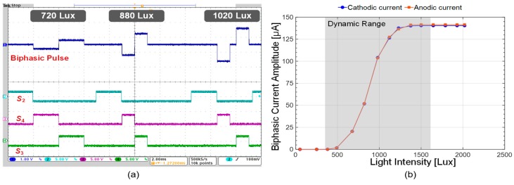
Figure 3 shows a micrograph of the 64-pixel stimulator array adopting the proposed architecture, and the global digital controller to produce digital signals for S1, S2, S3, S4 and S5 in Figure 2a; both were fabricated in a single chip using a standard 0.35-µm 4M2P CMOS process. This full chip occupies an active area of 4.3 × 3.2 mm2. We first conducted a benchtop experiment to measure the transient bip-hasic current waveforms, which vary with the incident light intensity, using a light source (Model: Newport 66088-LED). Figure 4a illustrates the biphasic current waveform and its digital control signals observed with an oscilloscope (Model: Tektronix MSO4104). By changing the light intensity and supplying various digital pulses to the SPStim, we successfully generated diverse biphasic current shapes in amplitude, width, interphase and period. In this benchtop experiment, we used a 10-kΩ resistor to simply mimic the electrode resistance and set the time width for S2 to 2 ms for fair comparison of the light-dependent biphasic current amplitudes.
Figure 3.
(a) Layout of the global digital controller embedded onto the signal chip with a 64-pixel stimulator array (its active area is gauged as 441.5 × 425.5 μm2); (b) micrograph of the 64-pixel stimulator array; (c) layout of the proposed single-pixel stimulator, which occupies an active area of 114 × 117 μm2.
Figure 4.
(a) Measured transient waveforms for the biphasic current and digital input pulses, where a 10-kΩ resistor was used to model the electrode resistance; (b) anodic and cathodic current amplitudes varying with incident light intensity.
Figure 4b shows the measured anodic (red line) and cathodic (blue line) amplitudes relying on the incident light intensity.
The observed results show that the biphasic stimulus current of the proposed SPStim varies from 0 to 143 μA in the dynamic range from 400 to 1600 lux, where an average mismatch of 1.12% was calculated using the following equation.
| (8) |
Here, N, Aanodic and Acathodic indicate the number of measured samples, the anodic and cathodic pulse amplitudes in the dynamic range. This low mismatch is due to the switched-capacitor current mirror technique described in Figure 2a. The charge remaining on the tissue after stimulation was completely removed by turning on the charge-balancing switch M15.
Next, we ex-vivo demonstrated the proposed SPStim using a dissected pig eyeball as shown in Figure 5. Here, it is observed that the biphasic pulse amplitudes are reduced by approximately 29% compared to the waveforms measured in Figure 4a. This is because the incident light intensity is attenuated when passing through the pig eyeball lens [17]. In terms of Equation (1), the attenuated light reduces IDARK in the photodiode, thereby reducing the stimulation current IPD. To compensate for the reduced IPD, we elongated the S2 (ΔT in Equation (1)) from 2 ms (see Figure 4a) to 2.5 ms, and as a result, the SP-Stim could generate the same biphasic pulse amplitudes as observed in Figure 4b in the same dynamic range. This demonstration shows that the customized global digital controller is necessary to adjust biphasic stimulus pulses after implantation. Finally, the overall performance of the proposed SPStim is summarized in Table 1.
Figure 5.
(a) Illustration of the ex-vivo demonstration setup; (b) ex-vivo experiment using a dissected pig eyeball.
Table 1.
Electrical performance Summary and comparison of the proposed single-pixel stimulator (SPStim).
| [18] | [6] | [12] | [13] | [3,18,19,20] | This Work | |
|---|---|---|---|---|---|---|
| CMOS Process | 0.35-μm standard | 0.18-μm CIS ** | 0.18-μm CIS ** | 0.35-μm BCD *** | 0.35-μm CIS ** | 0.35-μm standard |
| Supply voltage [V] | 5 | ± 1.65 | 0.5, 1.8 | 5, 12 | ± 2 | ± 1.65 |
| Chip area [mm2] | 1.0 × 2.7 | 2.2 × 2.2 | 1.9 × 1.9 | 2.5 × 1.2 | 3 × 3.5 | 4.3 × 3.2 |
| Single pixel area [μm2] | 200 × 200 | 127 × 167 | 30 × 30 | 55 × 50 | 30 × 30 | 114 × 117 |
| Dynamic range [Lux] | - | 400–1200 | 1–1000 | 100–250 | 0.1–10,000 | 400–1600 |
| Pulse amplitude * [μA] | 50–1050 | 0–343 | 0–50 | 0–300 | 0–100 | 0–143 |
| On-chip digital controller | Yes | No | Yes | No | Yes | Yes |
| Pulse width * [ms] | - | - | - | - | 4 | 0.5–5 |
| Pulse period * [ms] | - | - | 60 | - | 3–100 | 1–50 |
| Interphase delay * [ms] | - | - | - | - | 0 ms | 0–2 ms |
| Mismatch [%] | - | 4.85 | - | - | - | 1.12 |
| Stimulation method | Charge-balanced biphasic current stimulation | |||||
* Pulse: Biphasic Pulse, ** CIS: CMOS Image Sensor, *** BCD: Bipolar CMOS and Double diffused MOS(DMOS).
4. Conclusions
A fully integrated low-power and low-mismatch SPStim was designed for subretinal implants. By adopting two switched-capacitor current mirrors for anodic and cathodic pulse generation, in this work, we achieved relatively less power consumption, compared to a SPStim using the additional current-mirror branch to generate an anodic or a cathodic stimulation pulses, and low mismatch to decrease the residual charges that can have deleterious effects on the retina. Using the customized P+/N-well photodiode in a standard CMOS process also enabled relatively lower fabrication cost than a complex CMOS images sensor process. The 64-pixel stimulators employing the proposed architecture were fabricated in a standard 0.35-μm CMOS process and ex-vivo tested with a dissected pig eyeball. From the measured results, the device achieves a maximum biphasic pulse amplitude of 143 μA, an output dynamic range of 86.7%, and a mismatch of 1.12% on average between the anodic and cathodic pulses. The customized global digital controller, for producing diverse biphasic stimulus currents in amplitude, width, interphase delay, and period, was embedded on the same chip with the 64-pixel stimulators and used to compensate for the attenuated light intensity passing through the pig eyeball lens in ex-vivo experiments. In future work, a refined 64-pixel stimulator array will functionalize the wireless power and data telemetry that we are developing now.
Acknowledgments
The authors are grateful to the IC Design Education Center (IDEC) for chip fabrication.
Author Contributions
The individual contributions of authors are follows: H.K. designed the stimulator chip and wrote the manuscript. W.H.A. designed the on-chip digital controller and took part in the manuscript revision. S.-W.K. conducted the ex-vivo experiment using the dissected pig eyeball. J.K. managed the project.
Funding
This research was partially supported by the National Research Foundation of Korea (Grant No. NRF-2017M3A9E2056461) and the Gachon University Gil Medical Center (Grant No. 2016-16).
Conflicts of Interest
The authors declare no conflict of interest.
References
- 1.Ortmanns M., Rocke A., Gehrke M., Tiedtke H. A 232-Channel Epiretinal Stimulator ASIC. IEEE J. Solid-State Circuits. 2007;42:2946–2959. doi: 10.1109/JSSC.2007.908693. [DOI] [Google Scholar]
- 2.Chen K., Yang Z., Hoang L., Weiland J., Humayun M., Liu W. An Integrated 256-Channel Epiretinal Prosthesis. IEEE J. Solid-State Circuits. 2010;45:1946–1956. doi: 10.1109/JSSC.2010.2055371. [DOI] [Google Scholar]
- 3.Rothermel A., Liu L., Aryan N.P., Fisher M., Wuenschmann J., Kibbel S., Harscher A. A CMOS Chip with Active Pixel Array and Specific Test Features for Subretinal Implantation. IEEE J. Solid-State Circuits. 2009;44:290–300. doi: 10.1109/JSSC.2008.2007436. [DOI] [Google Scholar]
- 4.Ng D.C., Furumiya T., Yasuoka K., Uehara A., Kagawa K., Tokuda T., Nunoshita M., Ohta J. Pulse frequency modulation based CMOS image sensor for subretinal stimulation. IEEE Trans. Circuits Syst. II Express Briefs. 2006;53:487–491. doi: 10.1109/TCSII.2006.875334. [DOI] [Google Scholar]
- 5.Boinagrov D., Lei X., Goetz G., Kamins I.T., Mathieson K., Galambos L., Harris S.J., Jr., Palanker D. Photovoltaic Pixels for Neural Stimulation: Circuit Models and Performance. IEEE Trans. Biomed. Circuits Syst. 2016;10:85–97. doi: 10.1109/TBCAS.2014.2376528. [DOI] [PMC free article] [PubMed] [Google Scholar]
- 6.Park H., Shim S., Jeong J., Kim S. A Multi-photodiode Array-based Retinal Implant IC with On/off Stimulation Strategy to Improve Spatial Resolution. JSTS J. Semicond. Technol. Sci. 2017;17:35–41. doi: 10.5573/JSTS.2017.17.1.035. [DOI] [Google Scholar]
- 7.Ayton L.N., Blamey P.J., Guymer R.H., Luu C.D., Nayagam D.A. First-in-Human Trial of a Novel Suprachoroidal Retinal Prosthesis. PLoS ONE. 2014;9:e115239. doi: 10.1371/journal.pone.0115239. [DOI] [PMC free article] [PubMed] [Google Scholar]
- 8.Zrenner E., Bartz-Schmidt K.U., Besch D., Gekeler F., Koitschev A., Sachs H.G., Stingl K. The Subretinal Implant ALPHA: Implantation and Functional Results, Artificial Vision: Clinical Guide. Springer international Publishing; Berlin, Germany: 2017. pp. 65–83. [Google Scholar]
- 9.Cheng D.L., Greenburg P.B., Borton D.A. Advances in Retinal Prosthetic Research: A Systematic Review of Engineering and Clinical Characteristics of Current Prosthetic Initiatives. Curr. Eye Res. 2017;42:334–347. doi: 10.1080/02713683.2016.1270326. [DOI] [PubMed] [Google Scholar]
- 10.Merrill D.R., Bikson M., Jefferys J.G.R. Electrical stimulation of excitable tissue: Design of efficacious and safe protocols. J. Neurosci. Method. 2004;141:171–198. doi: 10.1016/j.jneumeth.2004.10.020. [DOI] [PubMed] [Google Scholar]
- 11.Humayun M.S., Juan E., Jr., Weiland J.D., Dagnelie G., Katona S., Greenberg R., Suzuki S. Pattern electrical stimulation of the human retina. Curr. Eye Res. 1999;39:2569–2576. doi: 10.1016/S0042-6989(99)00052-8. [DOI] [PubMed] [Google Scholar]
- 12.Chih-Lin L., Chih-Cheng H. A 0.5 V/1.8 V High Dynamic Range CMOS Imager for Artificial Retina Applications. IEEE Sens. J. 2015;15:6833–6838. [Google Scholar]
- 13.Oh S., Ahn J., Lee S., Ko H., Seo J., Goo Y., Cho D. Light-Controlled Biphasic Current Stimulator IC Using CMOS Image Sensors for High-Resolution Retinal Prosthesis and in-vitro Experimental Results with rd1 Mouse. IEEE Trans. Biomed. Eng. 2015;62:70–79. doi: 10.1109/TBME.2014.2336799. [DOI] [PubMed] [Google Scholar]
- 14.Kartikeya M., Ralph E., Nitish T., Gert C. Which photodiode to Use: A Comparison of CMOS-Compatible Structure. IEEE Sens. J. 2009;9:752–760. doi: 10.1109/JSEN.2009.2021805. [DOI] [PMC free article] [PubMed] [Google Scholar]
- 15.Köklü G., Etienne-Cummings R., Leblebici Y., Micheli G., Carrara S. Characterization of standard CMOS compatible photodiodes and pixels for lab-on-chip devices; Proceedings of the IEEE International Symposium on Circuits and Systems; Beijing, China. 19–23 May 2013; pp. 1075–1078. [Google Scholar]
- 16.Zhang L., Wang Z.-H., Li Y.-M., Zhang C., Wang Z.-H., Chen H.-H. Clock generator and OOK modulator for RFID application. J. Zhejiang Univ. Sci. 2005;6A:1051–1053. [Google Scholar]
- 17.Seo H., Nam D., Lee J., Park S., Kim Y., Kim S., Chung T., Inoue M., Kim T. Macular photostress and visual experience between microscope and intracameral illumination during cataract surgery. J. Cataract Refract. Surg. 2018;44:190–197. doi: 10.1016/j.jcrs.2017.11.016. [DOI] [PubMed] [Google Scholar]
- 18.Tokuda T., Hiyama K., Sawamura S., Sasagawa K., Terasawa T., Nishida K., Kitaguchi Y., Fujikado T., Tano Y., Ohta J. CMOS-Based Multichip Networked Flexible Retinal Stimulator Designed for Image-Based Retinal Prosthesis. IEEE Trans. Electron Devices. 2009;56:2577–2585. doi: 10.1109/TED.2009.2030552. [DOI] [Google Scholar]
- 19.Rothermel A. Recent results with subretinal stimulation; Proceedings of the IEEE Biomedical Circuits and Systems Conference (BioCAS); Lausanne, Switzerland. 22–24 October 2014; pp. 220–223. [Google Scholar]
- 20.Liu L., Wiinschmann J., Aryan P.N., Zohny A., Fischer M. An ambient light adaptive subretinal stimulator; Proceedings of the 2009 ESSCIRC; Athens, Greece. 14–18 September 2009; pp. 420–423. [Google Scholar]


