Figure 2.

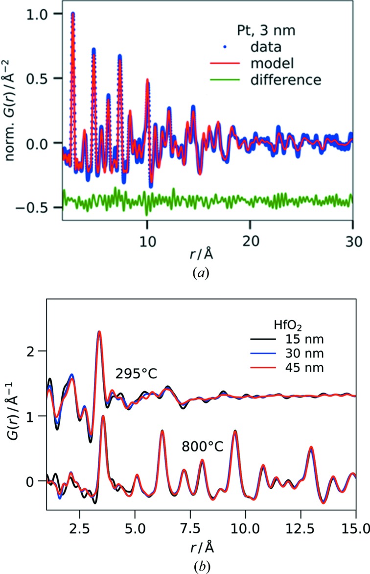
(a) PDF data and refinement of a 3 nm sputter-deposited Pt layer on fused silica; R w = 24% for the r fitting range 1.75–60 Å (shown only to 30 Å for clarity); (b) PDFs of HfO2 thin films of different thicknesses on fused silica deposited by chemical solution deposition and heat-treated at the indicated temperatures [offset in G(r) for clarity]. The film thickness increases in steps owing to the preparation by stacking multiple coatings of 15 nm each, i.e. the samples correspond to 1, 2 and 3 coatings, respectively.
