Abstract
Design and successful implementation of a fully-integrated CMOS fluorescence biochip for DNA/RNA testing in molecular diagnostics (MDx) is presented. The biochip includes a 32×32 array of continuous wave fluorescence detection biosensing elements. Each biosensing element is capable of having unique DNA probe sequences, wavelength-selective multi-dielectric emission filter (OD of 3.6), resistive heater for thermal cycling, and a high performance and programmable photodetector. The dimension of each biosensor is 100µm×100µm with a 50µm×50µm Nwell-Psub photodiode acting as the optical transducer, and a ΣΔ modulator based photocurrent sensor. The measured photodetector performance shows ~116 dB detection dynamic range (10fA – 10nA) over the 25°C – 100°C temperature range, while being ~1 dB away from the fundamental shot-noise limit. To empirically demonstrate the compatibility of this biochip with MDx applications, we have successfully utilized the array and its thermal cycling capability to adopt a 7-plex panel for detection of 6 human upper respiratory viruses.
Index Terms: Biosensor, Fluorescence Spectroscopy, Microarray, Molecular Diagnostics, Optical Filter, Biochip, Polymerase Chain Reaction, Nucleic Acid, Infectious Disease, Image Sensors
I. Introduction
Leveraging the specificity of bio-molecular interactions to detect the presence and abundance of biological analytes such as DNA, proteins, toxins, hormones and other biomolecules is the underlying principle of biosensing [1]. Today, there are a multitude of biosensors categorized by their probe structure and transduction mechanism (e.g., optical [2–6], electronic [7–8], or mechanical [9–10]). Yet, the most widely used biosensors include DNA or antibody probes and adopt optical readouts, specifically continuous wave (CW) fluorescence transduction methods [4–6, 11–12]. Such broad choice of probes is mainly due to the versatility of DNA and antibody probes and the available methods to biochemically synthesize or engineer them to recognize “almost” any target analyte biomolecule [13–14]. The rationale behind using the CW fluorescence method is the availability of versatile fluorophore molecules as molecular tags (labels) [15] to identify and quantify bio-molecules. Fluorescent labels, unlike their electrochemical, mechanical, or magnetic counterparts, are bio-compatible, are easy to adopt in molecular biology, are easy to conjugate with probes and target analytes, have a high detection contrast (i.e., high signal-to-background in aqueous medium), have multiple colors, and are measurable using conventional microscopy instrumentation and scanners.
Here, we present an integrated CMOS biosensor array (biochip), designed and implemented specifically for CW fluorescence detection and nucleic acid (DNA or RNA) testing. In the past decade, there has been numerous reported CMOS biochips utilizing non-optical techniques such as electro-analytical [16–18] and magnetic [19–20]. One can correctly claim that such non-optical biochips offer superior transducer compatibility for integration in standard CMOS. Nevertheless, such biosensors by and large require unconventional labels that offer no “color” and cannot be used in real-time detection assays that are common in molecular biology. Moreover, bio-compatible surfaces (e.g., SiO2, or Si3N4) are not always compatible with non-optical transducers. Examples are CMOS electro-analytical biosensors that require Faradaic electrodes built using Au or Pt [21, 22]. Hence, their adoption in applied fields such as molecular diagnostics (MDx), genomics and proteomics research will be inferior to biochip platforms utilizing “gold standard” fluorescence techniques.
The focus of this paper is the system level design of the CMOS biochip and the implementation techniques to satisfy the stringent requirements of state-of-art DNA/RNA detection assays in MDx. In Section 2, we first present the formulations and theoretical models of on-chip CW fluorescence-based detection. Next, we discuss the proposed system architecture which includes the integrated circuit components, the reaction chamber, surface chemistry and the assay. In Section 3, we discuss the circuit design implementation of the system in detail and report its measured performance, followed by Section 4, in which we explain the post-CMOS fabrication steps. In Section 5, we report a successful implementation of an MDx panel for upper respiratory viruses using a polymerase chain reaction (PCR [23]) based assay.
II. Specifications
A. CW fluorescence detectors
Fluorescence-based detection relies on excitation of electrons in the valence band of unique molecules (fluorophores [24]) by applying photon flux Fx at wavelength λx and detecting the return of the electrons to the ground state by monitoring the emitted photon flux Fe at wavelength λe (λx < λe). In fluorescence biosensors, depicted in Fig. 1, fluorophores are used as reporter molecules (labels) for the targets, while capturing probes are immobilized on a surface. The capturing of the targets by the probes results in aggregation of fluorophores on the surface which increases Fe at the probe coordinates.
Fig. 1.
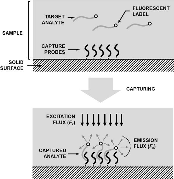
Fluorescence biosensor with immobilized capture probes for analyte detection.
To formulate this process, we use Beer-Lambert Law [25] which describes the transmitted photon flux, (photons cm−2 sec−1), through a medium with path length l (cm) that includes n absorbing fluorophore species in the sample with concentration Cn (M) as
| (1) |
where ε (cm−1M−1) is the fluorophore absorption (extinction) coefficient at λx. Now in biosensors (Fig. 2), all the fluorophores are immobilized at the surface (i.e., l → 0). Therefore, (1) becomes
| (2) |
where NA, ns, S are the Avogadro’s number, fluorophore surface concentration and surface area, respectively. The photon absorption rate in this situation, denoted by Ax, is formulated by
| (3) |
Now, assuming that QY (λe) is the quantum yield function of the fluorophore, described as the photon emission probability distribution function at λe, then the isotropic (in all directions) photon emission flux, Fe(λe), becomes
| (4) |
Fig. 2.
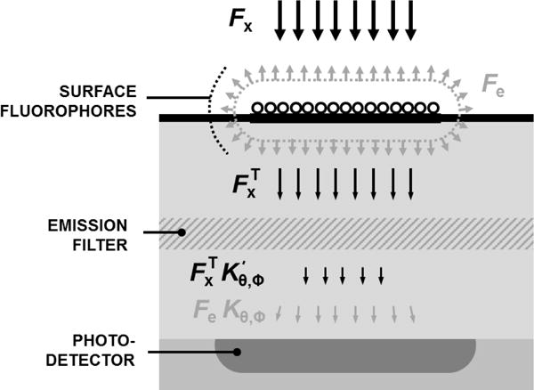
Simplified cross-section of a chip-based fluorescence biosensors system with an embedded photodetector beneath the capturing probe area.
As depicted in Fig. 2, we can introduce parameter Kθ,ϕ as the transmittance efficiency of Fe(λe) originated from probe area S, to the photodetector. If the quantum efficiency of the photodetector is QE(λ), then the emission-induced photocurrent, Iem, can be formulated by
| (5) |
where q is the charge of an electron. In practical systems, a fraction of Fx will always “leak” to the photodetector and create the background photocurrent, Ibk, such that
| (6) |
where is the transmittance efficiency of . By combining (5) and (6), we can thus derive the signal-to-background ratio of the system as
| (7) |
The significance of (7) is that it demonstrates the independence of Iem/Ibk to Fx. Furthermore, it demonstrates that the optimal approach to achieve high Iem/Ibk, is to increase , the wavelength selectivity of the detector as the other parameters in (7) (e.g., ε or ns) are constrained by the assay and the involved chemistry and not the detector.
Another important parameter to consider in our models is the signal-to-noise ratio (SNR). Providing a closed-form equation for SNR of a detector is involved; however, calculating its upper limit, SNRmax, generally referred to as the shot-noise limit, is straightforward. If we assume that the detector dark current is Idc, then SNRmax for the detection bandwidth of BW becomes
| (8) |
In Table I, we have provided some numerical examples to better illustrate the design tradeoffs according to the formulations above. As expected from (7), the wavelength selectivity (e.g., having a sharp emission filter) has a first-order effect on the SNR. Yet, at elevated temperatures, Idc, becomes significant. This indicates that photodetector is required to have a high detection dynamic range (DDR) to be able to measure Iem in presence of large Ibk + Idc values. It is also suitable to build a photodetector with an input-referred noise smaller than the shot-noise of the background with a R.M.S. value of .
TABLE I.
| A. Numerical examples of SNR and Signal-to-background ratio of a biosensor system. | |||||||||
|---|---|---|---|---|---|---|---|---|---|
| ns | Iem (A) |
|
Ibk (A) | T(°C) | Idc (A) |
|
SNRmax | ||
| 102 | 43f | 102 | 1.9n | 30 | 20f | 2.29×10⁻⁵ | 3.12 | ||
| 90 | 5.5p | 2.29×10⁻⁵ | 3.11 | ||||||
| 105 | 1.9p | 30 | 20f | 2.27×10⁻² | 3.02×10³ | ||||
| 90 | 5.5p | 5.89×10⁻³ | 7.97×10² | ||||||
| 104 | 4.3p | 102 | 1.9n | 30 | 20f | 2.29×10⁻³ | 3.12×10⁴ | ||
| 90 | 5.5p | 2.29×10⁻³ | 3.11×10⁴ | ||||||
| 105 | 1.9p | 30 | 20f | 2.27 | 9.45×10⁶ | ||||
| 90 | 5.5p | 0.589 | 5.05×10⁶ | ||||||
| B. Parameters | |||
|---|---|---|---|
| Parameter | Value | Parameter | Value |
| Photon flux density (Fx) | 5×1017 cm−2 s−1 | Max. quantum yield (QY(λe))1 | 0.04 |
| Probe surface area (S) | 2500 μm2 | Transmittance efficiency (Κθ ϕ) | 0.25 |
| Diode surface area | 2500 μm2 | Max. photodiode QE2 | 0.38 |
| Max. extinction coefficient (ε)1 | 150,000 cm−1M−1 | Detection bandwidth (BW) | 1 Hz |
Values are for Cyanine-3 (Cy3) fluorophore [20].
Typical value for Nwell-Psub diode in 0.25µm CMOS process
B. DNA/RNA testing
Generally speaking, DNA/RNA analytes and probes have little bearing on the optical design of fluorescence biosensors as they only show absorption at wavelengths < 310 nm [26], which ensures their non-interference with fluorescence detection within the 450–800 nm “useful” range. However, there are key specifications with respect to DNA probe immobilization that the biochip should always meet to ensure compatibility with DNA/RNA testing assays in MDx. The first is having a SiO2 surface in contact with the aqueous sample [27]. The second requirement is the thermal stability of probes in pH buffer solutions (e.g., PBS or TBS [28]). The probes need to be stable up to 95°C to enable DNA/RNA amplification assays such as PCR processes [23]. The third specification is related to maximum probe density for target accessibility. In the case of DNA microarrays the “optimal” distance is suggested to be 6–9 nm (~1.2−2.8×104 µm−2) [27].
The number of elements within a biosensor array is a function of the number of analytes that one needs to detect multiplied by the required redundancy. In our CMOS biochip system, we have chosen to implement an array with 1024 (32 × 32) elements which is aligned with applications in MDx rather than life science research [29–30].
C. Proposed architecture
In Fig. 3a, we show the proposed and implemented biochip module, which includes a CMOS IC, integrated emission filter, DNA probes, and an optically transparent fluidic cap which not only confines the aqueous sample on top of the chip, but also facilitates its insertion and removal using an inlet port and an outlet port, respectively. The CMOS IC not only provides the high DDR photocurrent sensing, but also integrated heating and temperature sensing. The biochip and the fluidic cap are both assembled on a single PCB substrate with an edge I/O connector on its periphery to access the chip electronics.
Fig. 3.
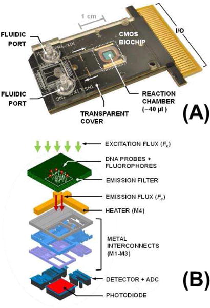
(a) Implemented biochip module; and (b) functional layers of an integrated CW fluorescence-based biosensor element (pixel).
In Fig. 3b, we illustrate the functional layers of an integrated CW fluorescence-based biosensor element and in Table II we listed the key system requirements and their justifications. The DNA capture probes are immobilized on top of the filter (surface SiO2). The fluorophores are located within the probe regions and are excited by an external LED-based photon flux that passes through the fluidic cap and the sample. Beneath the filter, we have the IC metal layers (4 metal layers in our 0.25 µm CMOS process). The top metal (M4) includes a passive heater structure, while M1-M3 are used as interconnects as well as creating an optical aperture for an Nwell-Psub.
TABLE II.
Biochip Requirements
| Parameter | Value | Justification |
|---|---|---|
| Biosensor dimensions | 100μm×100μm | Min. pitch for surface spotting
techniques. Min. area for high DDR ΣΔ modulator. |
| No. of biosensing elements | 1024 (32×32) | Enables infectious disease MDx
applications. Capable of running 100–200 NAAT tests with sufficient redundancy. |
| Detection dynamic range (DDR) | >100dB | Need to detect ID ~ 20fA-10nA (Table 1A). |
| Frame rate | ~1Hz | Suitable for monitoring DNA hybridization reaction (τ > 30s). Sufficient OSR for high DDR ΣΔ operation. |
| Operating temperature | 25°C – 100°C | Required for PCR (Fig. 14). |
| Quantum efficiency (QE(λ)) | > 0.2 for 500nm ≤ λ ≤ 600nm | Required for sufficient Iem values (Table 1A). |
| Max. input photocurrent | 10nA | Max. Ibk + Idc (Table 1A). |
| Min. input photocurrent | 10fA | Min. Iem (Table 1A). |
| Photodetector noise contribution | < Shot-noise | Fundamental noise limit for a current sensor (Section 3.2.1). |
| Temperature sensor resolution | < 0.5°C | Accuracy of PCR machines ~ ± 0.25°C [23]. |
| On-chip heater power | 10W | Required for achieving > 5°C/s ramp rates for PCR [23]. |
| Chip output format | Digital | Greatly simplifies array output data handling. |
| Optical filter rejection | >103.5 at λ = 490 nm | Necessary for sufficiently high (signal to background) ratio (Table 1A). |
|
|
>1000 | |
| Top surface material | SiO2 | Most suitable for thermo-stable DNA probe immobilization [27] (Section 2.2). |
| Surface probe density | ~ 1.2−2.8 × 104 μm−2 | Optimal distance for target accessibility (Section 2.2). |
III. Circuit implementation
A. Photodetector Implementation
In our biochip, we implemented a 1st-order ΣΔ current-sensing modulator as the detector and a reverse-biased CMOS Nwell-Psub diode as the photon-to-electron transducer [31] within each biosensing element. The sensor input is the reverse-biased diode current, ID = Iem + Ibk + Idc, which first feeds into a high DC gain integrator (Σ operator) followed by an ADC (quantizer), as shown in Fig. 4a. The digital output of the ADC which is the sensor output, also controls a DAC to subtract an output-dependent current from the input (Δ operator).
Fig. 4.
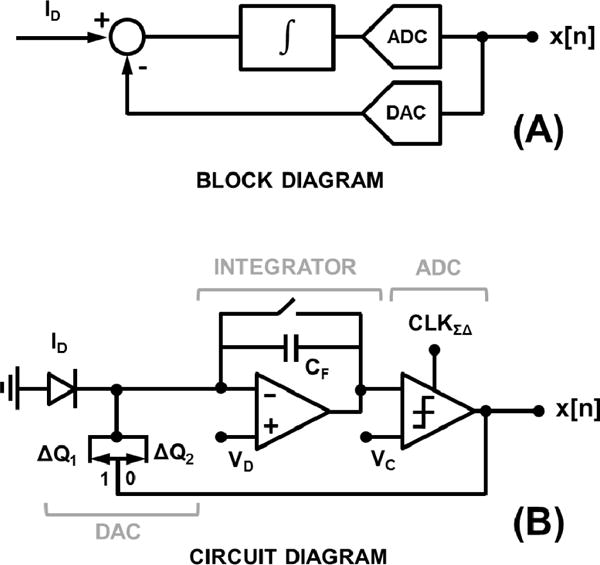
(a) Photo-detector block diagram; and (b) its circuit diagram.
There are multiple advantages of adopting this architecture in our system. First, it can achieve very high DDR (>100dB [32]) compared to 3T or 4T architectures used CMOS image sensor [33–34]. Second, it achieves superior noise performance due to ΣΔ operation [35–37]. Third, the architecture provides a digital output that can be easily read sequentially (scanned) in an array format. Finally, it can be easily integrated in the allocated 100µm × 100µm allocated silicon area. The disadvantages are the need for large oversampling ratios (OSR) and a fast oversampling clock to obtain the high DDR and the presence of idle-tones for very low input currents [38].
The high-level circuit diagram of the photodetector is shown in Fig. 4b. The integrator is a capacitive transimpedance amplifier (CTIA) which integrates ID on its feedback capacitor, CF, while pinning the reverse-bias voltage of the photodiode to VD. The ADC is a clocked comparator, comparing the output of the CTIA with VC, at every oversampling clock, CLKΣΔ, which has the frequency of fΣΔ. The current DAC is implemented as a charge packet subtractor, which depending on the comparator output being 1 or 0, subtracts ΔQ1 or ΔQ2 from the CTIA input, respectively. It is important to note here that the ΣΔ modulator is insensitive to the offset at the VC node as the offset is suppressed by its noise transfer function (NTF), given by equation (9), where f is the frequency[38]. In our system, we set VC = VD.
| (9) |
In Fig. 5, we show the detailed transistor and gate-level circuit implementation of the photodetector and its timing diagram. The core element of CTIA is a folded-cascode operational trans-conductance amplifier (OTA) with an open loop gain of ~80dB and an output swing between 0.5–2V. The capacitive feedback path of the integrator has the option to place CF1(20fF) or both CF1 and CF2 (180fF) in the feedback loop by using the gain switch transistors MN10-MN11. A two-transistor switch structure MN7-MN8 with a keeper switch MN9 is used for resetting and ensuring output-independent leakage current.
Fig. 5.
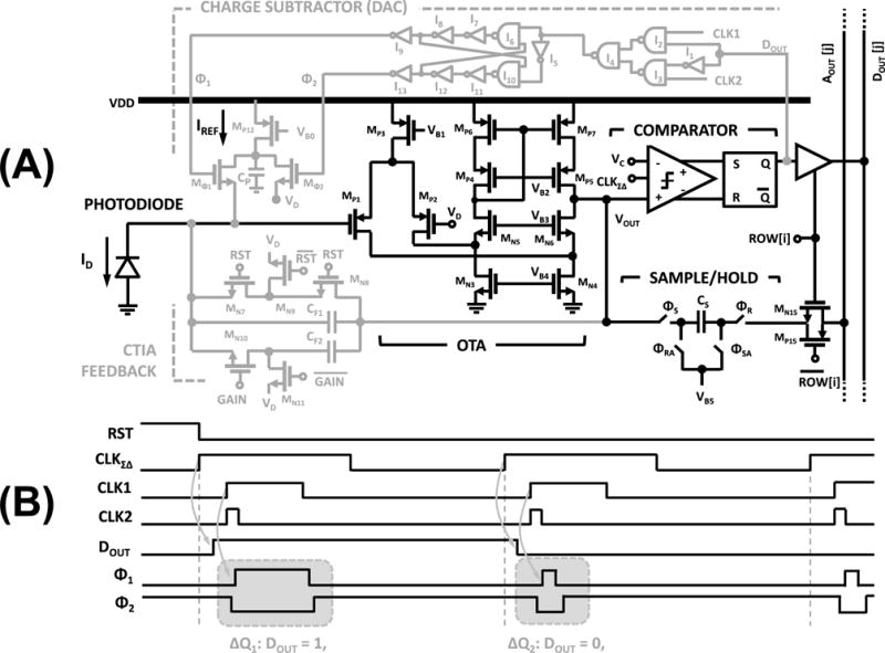
(a) Detailed circuit schematic of the photodetector; and (b) its timing diagram.
A Yukawa clocked comparator [39] is utilized for comparing VOUT, output of the CTIA, with input Vc on the rising edge of CLKΣΔ. Its output is then captured by an S–R latch, creating DOUT, that can be read through column line DOUT [j] when ROW [i] is selected.
The charge subtraction DAC path consists of a fixed current source, generating IREF, and a pulse generator circuit applying IREF periodically, in short pulses, to the CTIA input terminal. In this circuit, M Φ1 and M Φ2 serve as the current steering switches, i.e., when Φ1 = 1 and Φ2 = 0, the current is steered into the CTIA input, to perform the charge = subtraction operation. When Φ1 = 0 and Φ2 = 1, the current sinks into VD node. The pulse generation circuit first selects between CLK 1 and CLK2 depending on whether DOUT is 1 or 0 respectively using gates I1–I4. The resulting output is then used to generate non-overlapping current steering signals, Φ1 and Φ2. The timing diagram of the system is shown in Fig. 5. Depending on CLK1 and CLK2, the applied pulse durations for current steering pulses are tp1 and tp2, corresponding to subtracted charge of ΔQ1 = tp1IREF and ΔQ2 = tp2IREF from the charge stored in CF.
As shown in Fig. 5, an analog bottom-plate sampling circuit has also been implemented for the test mode. This circuit samples VOUT onto a sampling capacitor CS (100fF) which can then be read though the column analog output line AOUT [j], when ROW[i] is selected. The analog sampling circuit is used for debugging and characterization in the test mode. In this mode, one can directly observe VOUT to measure voltage and charge distribution offsets.
In Fig. 6a and Fig. 6b, we show the layout and micrograph of the implemented photodetector. The total area is 100µm × 100µm with a photodiode fill-factor of 25%.
Fig. 6.
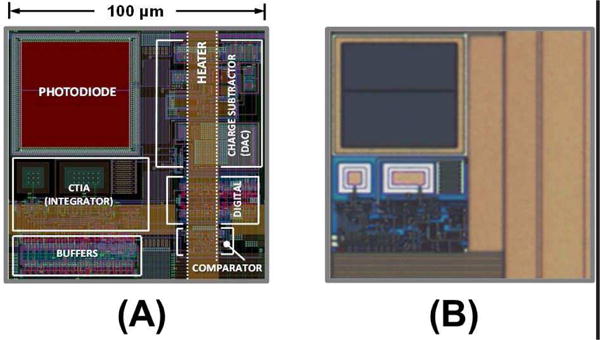
(a) Biosensing element (pixel) layout; and (b) its micrograph.
B. Photodetector theoretical performance
1) Saturation level (well capacity)
The maximum detectable input current, , occurs when the ΣΔ modulator feedback is continually subtracting, where
| (10) |
Consequently, the “well capacity”, Qwell, for sampling period of Ts = 1/BW and oversampling ratio, OSR = fΣΔ Ts, becomes
| (11) |
In our design, IREF is set to 1µA, fΣΔ = 100KHz, and tp1 can be programmed to be 100ns (low gain) or 10ns (high gain), making equal to 10nA or 1nA, respectively.
2) Noise formulations
The main noise contributors in this photodetector are the photodiode and the current DAC. The total fluctuation in ID can be formulated in the form of shot noise. The variance of the current fluctuations, is computed by
| (12) |
To derive the noise contribution of current DAC, we need to first consider the feedback current, IΔ(t) as the multiplication of IREF and a current switching pulse train p (t). Assuming that αi’s to be the fourier series coefficients of p (t) and fP being its fundamental frequency, it can shown that the , the power spectral density (PSD) of IΔ(t) is
| (13) |
which can be used to formulate, the variance of the noise contributed DAC, by
| (14) |
In our design, we considered the design criteria of to ensure that the photodetector be shot-noise limited. The consequence of that, is that the transistor sizes become large in the current source to reduce the flicker-noise of IREF.
C. Array architecture
The top-level chip architecture of the biochip and the die photo are shown in Fig. 7a and Fig. 7b, respectively. The biochip has an array of 32×32 pixels including 13 temperature sensor pixels. These 13 temperature sensor pixels have the same circuitry as regular pixels, except that we cover the in-pixel photodiode with metal to block and use Idc to measure the temperature. The temperature dependence of Idc [40] is given by
| (15) |
where I0 is a constant, Eg is the bandgap energy, k is the Boltzmann constant, x is a number between 1 and 2, and T is the absolute temperature.
Fig. 7.
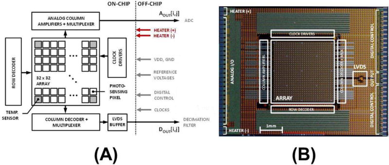
(a) Chip architecture; and (b) die micrograph.
Each element can be individually addressed through row and column decoders. The column multiplexer output DOUT [i, j] signal is sent off chip through low voltage differential signaling (LVDS) buffer. The analog output chain makes use of analog column amplifiers, which are multiplexed at column level to generate the AOUT [i, j] signal. All the clocks, row and column select signals, the analog reference voltages and power supply (3.3V) are applied from off chip.
The on-chip heating element is a 2.5Ω passive multi-finger metal resistor, implemented using the top metal layer (M4) to deliver up to 10W of power from a 5V source. The resistive lines are evenly distributed out across the chip, passing through both the array and its periphery.
D. Off-chip components and analysis
The reader electronics consists of a Spartan 6 XC6SLX16 FPGA, DACs, ADCs, chip edge connector, and drivers for the LED electronics and heater modules (Fig. 8). The single bit output data-stream Dout[n, i, j], is fed into an array of sinc2 filters in the FPGA for decimation and filtering. The FPGA then transfers the filtered data to the application software through a USB interface.
Fig. 8.
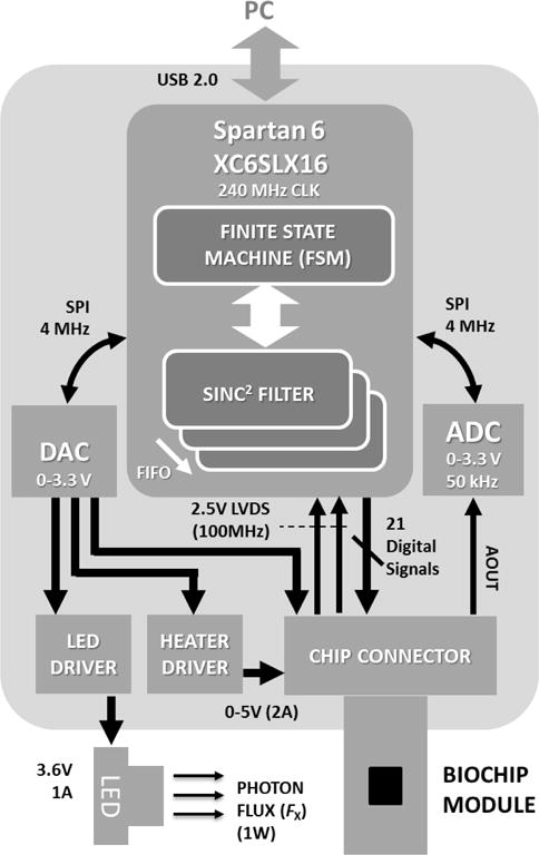
CMOS biochip module reader architecture and functional components.
In the experimental setup, we create Fx using a low power blue LED module (~1W of at 470nm). The chip is mounted on an active heat sink consisting of a copper heat spreader and a fan. The active heatsink arrangement facilitates fast cooling of the chip when the on-chip heater is off. The temperature of the reaction chamber mounted on chip is controlled using the on-chip heater, active heatsink, and the Idc temperature sensors.
One practical challenge in measuring low levels of photocurrent is the ever presence of Idc. To address this, we use correlated double sampling (CDS) scheme, implemented off-chip using the FPGA and the application software. The LED module is periodically turned on and off and frames are collected from the chip during both ON (“bright” frame) and OFF (“dark” frame) phase. The dark frames are used to estimate Idc and subtract it from ID to obtain the Iem + Ibk. To remove the non-informative Ibk from the measurements, we then make use of array elements where no probe is immobilized and use the estimated Ibk to derive Iem. To reduce the error in estimation of Ibk, we average Ibk of several neighboring pixels to reduce the effect of spatial variation and additionally, perform a gain calibration at each pixel site, by recording the pixel values at different LED intensities.
E. Measurement results
Fig. 9 shows the measured external quantum efficiency QE(λ) of the photodiode. In Fig. 10, we report the mean Idc measured across all pixels vs. temperature. A calibrated thermocouple was placed very close to the chip surface utilizing thermal epoxy to record the die temperature. The error bars specify the minimum and maximum Idc across the array measured at each temperature. Histograms of pixel dark current distribution at 30°C and 90°C are also shown in Fig. 10. As evident, at higher temperatures, “hot pixels” emerge at the outer edge of the array.
Fig. 9.
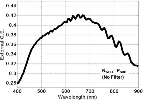
Measured external quantum efficiency of the photodiode.
Fig. 10.
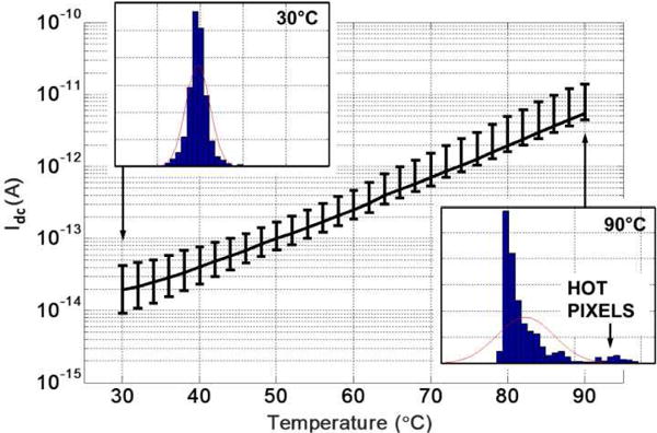
Measured photodiode dark current (Idc) vs. temperature along with minimum and maximum spatial variations.
Fig. 11 shows the linearity performance of the photodetector, defined as (ID − Idc) vs. Fx. Different Fx values were generated by utilizing a combination of neutral density filters (101–106 attenuation) along with varying LED power settings. Measurements were taken using two different modes: (a) low gain mode: tp1 = 100ns, ; and (b) high gain mode: tp1 = 10ns, . The OSR was set to 65535 with fΣΔ = 100kHz. As expected, we obtained very linear photo-detection performance, over 5 orders of magnitude change (~10fA - 10nA) in Fx.
Fig. 11.

Measured photodetector current vs. incident photon flux.
Fig. 12 shows both the simulated and measured SNR vs. Fx. The simulations adopt the formulations discussed in Section 3.2 to model the predicted SNR. Both the simulated and measured SNR drop from the shot-noise limit, near IQ, defined as the input-current quantization limit, given by . Below this limit, not even a single transition should occur in ΣΔ modulator during the entire CLKΣΔ period. The lower limit of Fxoccurs around 9 × 10⁹ photons cm−2 s−1 and 9 × 10¹⁰ photons cm−2 s−1 corresponding to IQ =15.2fA and 152fA for high gain and low gain modes, respectively. The SNR is close to its shot-noise limit at higher Fx, within ~1 dB. Deviation from the limit at Fx > 1012 photons cm−2 s−1, is believed to be due to additional fluctuation added by the LED excitation source and its driver electronics.
Fig. 12.
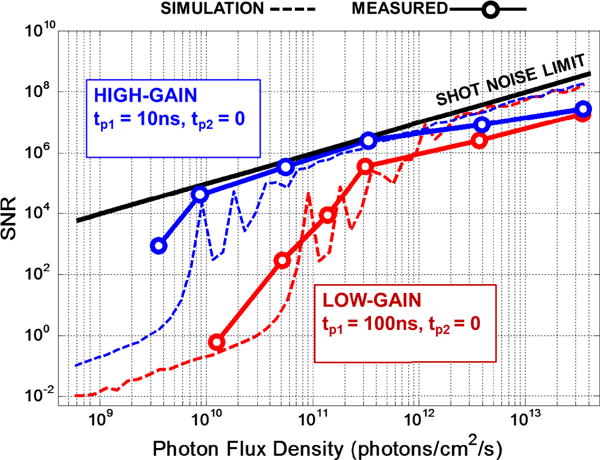
Measured and simulated SNR vs. photon flux for both high and low gain operating modes.
Table III summarizes the performance of the chip which matches the requirements that we set in Section 2. Measurement techniques for CMOS image sensor characterization [41] were used to perform the aforementioned measurements.
TABLE III.
Chip Performance Summary
| Technology | 0.25 μm CMOS |
| Supply voltage | 2.5V |
| Die dimensions | 7.0mm × 9.0mm |
| Array dimensions | 32 × 32 |
| Biosensor size | 100μm × 100μm |
| Photodiode | 50μm × 50μm (Nwell−Psub) |
| Photodetector dark current (Idc) | 20 fA (30°C)−5.5 pA (90°C) |
| Photodetector QE(λ) | >0.38 (500nm – 775nm) |
| Frame rate (BW) | 1Hz to 50Hz |
| Well capacity (Qwell) | 6.25 × 10¹⁰
e− (Low Gain) 6.25 × 10⁹ e− (High Gain) |
| Maximum photocurrent ( ) | 10nA (Low Gain) at
fΣΔ = 100 kHz 1nA (High Gain) at fΣΔ = 100 kHz |
| CLK1, CLK2 pulse width (tϕ1,2) | 10ns – 100ns |
| Detection linearity | >105 |
| Detection dynamic range (DDR) | 116 dB |
| Chip Output | 102.4 Mbps LVDS serialized |
| Heating/cooling rate | 4°C/sec |
| Operating temperature range | 25°C – 100°C |
| Temperature sensor resolution | 0.3°C (for chip temperature 45°C – 100°C) |
| Total power consumption | 62mW (array) + 50mW (LVDS) + 6mW (analog column amplifiers) = 118mW |
IV. Post-CMOS wafer/chip processing steps
There are two key processing steps that need to be done after the CMOS wafers are manufactured, to convert the CMOS chip into a biochip. The first is the fabrication and patterning of the multi-dielectric emission filter and the second is the bio-functionalization of the surface.
A. Emission filter
We utilize a long-pass multi-dielectric emission filter [42] to selectively reject Fx at λx and allow Fe to pass through. The filter is patterned and deposited on top of the CMOS wafer utilizing a lift-off process. The high and low index dielectric materials used for the filter are TiO2 and SiO2, respectively with the exposed filter surface (top surface) being SiO2. The filter coating is index matched to water at the peak of emission while the electric field at λx is maximized at the filter-water interface. The latter maximizes the surface-bound fluorophore excitation.
A disadvantage of interference filters is their high sensitivity to the angles of incidence (AOI). To address this challenge, we utilize a two-pronged solution. First, we have optimized the layer thicknesses in the emission filter to minimize AOI sensitivity. For optimization, we have extensively used Essential McLeod Software (Thin Film Center, Tucson AZ) and chosen the solution-filter interface layer to maximize the E-field. Second, we created a dual fluorophore construct that offers 85nm Stokes’ shift, defined as the distance between peak emission and excitation.
Fig. 13a shows the cross-section SEM of the emission filter. The total filter thickness is ~8µm. Fig. 13b shows the measured emission filter transmittance vs. wavelength at different AOIs. The on-chip filter characterization is done using a light source with a monochromator. The wavelength is swept between 400 and 700nm and the chip’s response to different wavelengths is recorded. In Fig. 13c, the measured excitation and emission spectrum of the fluorophore label is reported. The effective filter optical blocking ratio (OD) at λx = 490 nm (fluorophore peak excitation) is 3.6. For increasing AOIs up to 50°, the filter transmission band shifts only by 10 nm.
Fig. 13.
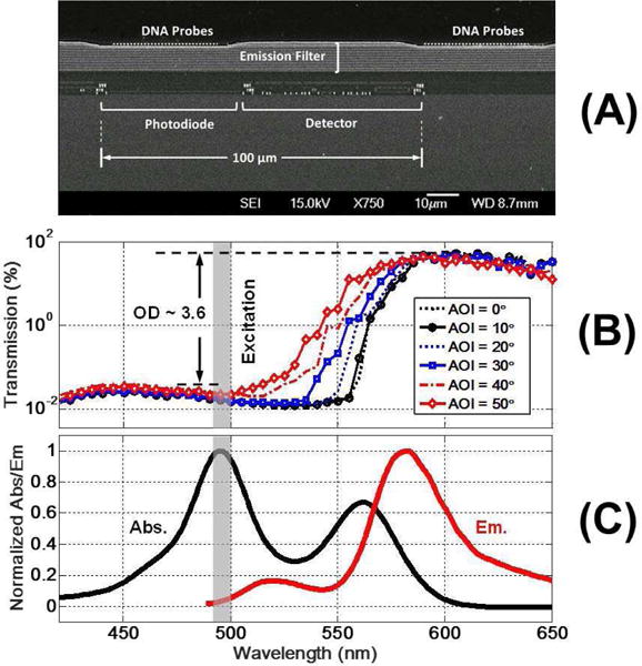
(a) Scanning electron microscope (SEM) cross-section of the chip + integrated filter; (b) measured filter transmittance vs. AOIs; and (c) excitation and emission spectrum of the dual fluorophore construct.
B. Surface bio-functionalization
CMOS chips bonded to FR4 PCBs are first cleaned using oxygen plasma and subsequently are exposed to (3-glycidoxypropyl) trimethoxysilane in a chemical vapor deposition (CVD) system without breaking vacuum. At this point, the covalently linked thin film bears epoxy functional groups that can react chemo-selectively with terminally labeled primary amine functionalities of synthetic DNA probes [43]. Non-contact piezo printing is then used to deposit ~80pL droplets of DNA solution onto individual photodetector elements at 100µm pitch. The printer’s integrated real-time vision system and optical fiducial registration capabilities allow drop placement accuracy verification within ±10 µm. Unreacted epoxy groups were rendered inert by treatment with a solution containing ethanolamine, a step that also removed excess (non-immobilized) DNA probes.
V. Assay implementation
To demonstrate the capabilities of our CMOS fluorescence biochip platform in detecting DNA/RNA from biological samples, we have successfully implemented a multi-analyte (multiplex) detection panel. This panel adopts a nucleic acid amplification testing (NAAT) method that includes PCR. The target analytes, to be detected by the chip, are seven common, unique respiratory pathogens listed in Table IV.
TABLE IV.
List of pathogens detected by NAAT panel along with the probe sequences used for solid-phase capturing and melt.
| Pathogen Name | Probe Sequence (5′-3′) |
|---|---|
| Influenza A (FluA) | Linker-GACCTAGTTGTTCTCGCCAGTGGAGGTCC-Fluor |
| Influenza B (FluB) | Linker-CACCGCAGTTTCAGCTGCTCGAATTGGGAGTTGAGGA-Fluor |
| Respiratory Syncytial Virus (RSV) | Linker-CTGTGTATGTGGAGCCTTCGTGAAGCTTCCATATTTGCC-Fluor |
| Human Parainfluenza Virus (HPIV) | Linker-GCGATTGATTCCATCACTTAGGTAAATTGGAAATGC-Fluor |
| Human Adenovirus C (AdvC2) | Linker-GCTCCACATAATCTAACACAAACTCCTCACCCCAGGTAAGATCGA-Fluor |
| Human Adenovirus E (AdvE) | Linker-TTTAATCATGGTTCTTCCTGTTCTTCCCTCCCAAATTGCA-Fluor |
| Polio (Positive Control) | Linker-TATCCGGTGAAAGTGAGATTCATTATCATTCGCTCCAT-Fluor |
| Negative Control | Linker-CAAAGTGGGAGACGTCGTTGT-Fluor |
In Fig. 14a, we show the chip workflow. In the first phase, during reverse transcription PCR (RT-PCR) enzymatic process [44], the sample goes through thermal cycling steps required to replicate (amplify) specific DNA/RNA sequence stretches (amplification factor >230) that are unique to individual pathogens in the sample. This is done by adding two short DNA sequences for each pathogen, generally referred to as primers, in the sample.
Fig. 14.
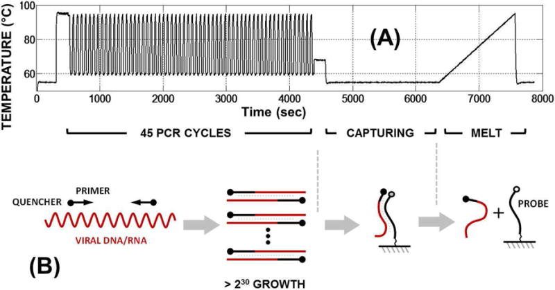
(a) Temperature profile for NAAT workflow with PCR cycling, capturing (hybridization), and melt steps; and (b) conceptual molecular diagram describing these three steps.
To enable the fluorescence detection of amplicons, we took advantage of an inverse fluorescence detection assay [45] (Fig. 14b). In this approach, all the PCR primers are labelled with quencher molecules (BHQ2) for incorporation into generated amplicons. To detect these amplicons, we spot fluorescent labeled DNA capturing probes (see Table IV), targeting individual amplicons, at fixed coordinates of the array (probe map shown in Fig. 15). During the capturing step, the generated amplicons hybridize to the corresponding probes on the array, bringing the quencher in close proximity of fluorescent labels, and thereby temporarily reducing the fluorescence at the particular location. Therefore, by monitoring the signal reduction at different spots in the array, one can identify the target(s) present in the original sample. In addition to the target specific capture probes, there are positive and negative control, quality control and calibration probes present in the array as shown in Fig. 15. The positive control provides an expected positive result due to the intentional addition of a known target nucleic acid to the reaction mix (Polio in our case). The negative controls work in the opposite manner, providing an expected negative result due to the absence of any corresponding target. Positive and negative controls help verify system functionality, determine repeatability and the level of non-specific signal in the system. Quality control probes are used to verify surface functionalization and DNA printing parameters. Calibration probes provide correction for fluorophore properties and any variation in LED illumination uniformity.
Fig. 15.
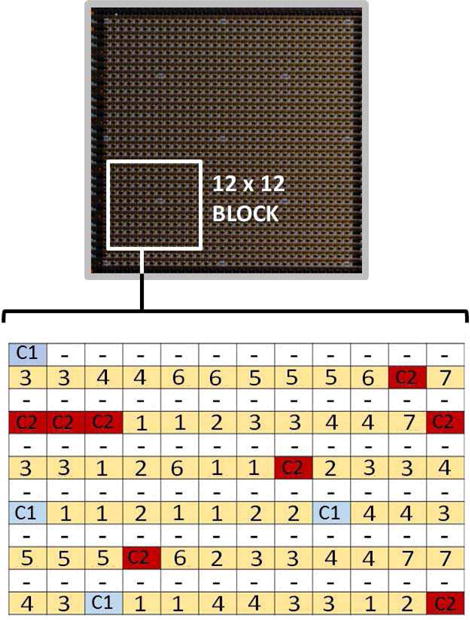
Probe map for a 12×12 biosensing block: (1) FluA, (2) FluB, (3) RSV, (4) HPIV, (5) AdvC2, (6) AdvE, (7) Pos. Ctrl, and (8) Neg. Ctrl. C1/C2 are quality control/calibration probes. White spots (–) are blank spots that can be used for Ibk subtraction.
To improve the specificity of the signal, we also perform a high-resolution melt (HRM) analysis [46] of the hybridized target-probe complexes to confirm that the correct target is reducing the signal at the corresponding probe coordinates. HRM analysis makes use of the fact that each probe-target DNA complex has a unique dissociation curve as a function of temperature (also known as the “melt” curve). This dissociation curve is a function of different properties of the DNA complex such as GC content, length, sequence and presence or absence of specific mutation and can serve as unique signature for a specific probe-target interaction. As shown in Fig. 14, the melt curve is performed by increasing the temperature from 55°C to 95°C and monitoring the return of the fluorescence signal as a function of temperature, as the probe-target complex ‘melts’ and the target DNA is dissociated from the surface bound complex.
In Fig. 16, we show the melt curve experimental results, including the array images and the relative fluorescence signal from different array elements for a sample containing FluA and FluB, for only the corresponding probes generate a melt curve signal and the negative control remained flat. In Fig. 17, we show averaged melt-curve results and the melting temperature Tm (defined as the temperature at which 50% of captured target-probe complexes detach from the surface), for all replicate spots, based on tests that include only one of the seven targets. The total time for experiment is ~2 hours, with ~1 hour of PCR cycling, ~0.5 hour of hybridization/capturing and ~0.5 hour of melt (Fig. 14a).
Fig. 16.
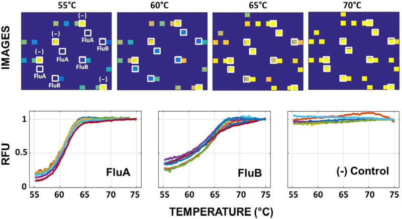
Measured melt curves for a sample containing FluA and FluB. The top images shows array snapshots at four different temperatures. The bottom set of images show the melt curves obtained from individual spots containing probes for FluA, FluB and negative control. The data is calibrated for temperature dependence of fluorophore intensity. It is expressed in relative fluorescence units (RFU).
Fig. 17.
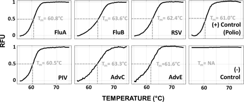
Average melt-curves from all the replicate spots for each of the seven pathogens and probes listed in table IV. Tm refers to the melt temperature, i.e. the temperature at which 50% of hybridized probe-target complex has melted from the surface.
VI. Conclusion
In this paper, we demonstrate both in theory and practice that CW biosensors can be built using standard CMOS processes, without compromising any performance requirement that is critical for adoption in MDx or genomics research. As reported, CMOS ICs can be designed to include integrated photo-detectors, thermal controllers, and all the essential electronic components; yet ICs do not offer any meaningful solution for the wavelength selectivity that CW fluorescence detection requires. As a result, we developed and integrated multi-dielectric interference filters to augment the photodetectors. The fabrication of these filters can easily be added to the CMOS process at a later stage.
When it comes to adopting “biology” on CMOS biochips, the focus should be on the surface and its bio-functionalization. In this paper, we show that conventional CVD techniques and non-contact printing methods can be utilized to create reliable and reproducible arrays of DNA probes. It is important to mention that at this point that these steps are not fully ready for high volume manufacturing. Therefore, their manufacturing cost are not comparable to the IC fabrication cost. However, with the reemergence of arrays in biotechnology and the current growth rate in MDx, we believe that this issue will be addressed by itself.
As a proof-of-principle, we reported the successful results of a NAAT panel in this paper. Clearly, the relatively small upper respiratory virus panel utilizes only a small fraction of the capabilities of our CMOS biochip. With 1024 biosensors in our chip, one can offer assays that can detect 100’s analytes simultaneously. This goal is exactly what we are aspiring to do and the next phase in this project.
Acknowledgments
The authors would like to thank Ruma Sinha for the bioinformatics design of primers and probe sequences, Nader Gamini and Piyush Savalia for the biochip package design and assembly.
Research reported in this publication was partially supported by National Human Genome Research Institute of the National Institutes of Health under award number 5R44HG007626-03. The content is solely the responsibility of the authors and does not necessarily represent the official views of the National Institutes of Health.
Biographies
Arun Manickam was born in Chennai, India in 1985. He received his B.E. degree in Electronics and Computer Engineering from College of Engineering, Guindy, Anna University in 2002, M.S.E. degree in Electrical Engineering from the University of Texas, Austin, TX, USA in 2008 and Ph.D. degree in Electrical Engineering from the University of Texas, Austin, TX, USA in 2012.
He has held engineering positions at Qualcomm, Silicon Laboratories and Bosch Research and Technology Center in 2007, 2008 and 2010 respectively. He co-founded InSilixa, a CMOS biochip company, where he is currently employed as an Engineering Manager. His primary research interests include biosensors and bioelectronics, specifically the design and development of CMOS biochip platforms for medical diagnostic applications.
Ritu Raj Singh received his B.Tech. in Electrical Engineering from the Indian Institute of Technology Kanpur, India, in 2005, the M.A.Sc. Degree in Electrical and Computer engineering from the University of Toronto, Canada, in 2009, and the Ph.D. Degree in Electrical and Computer engineering from the University of Texas at Austin, USA, in 2013.
He has held engineering positions with Texas Instruments, Mentor Graphics and Silicon Laboratories in 2004, 2005-2006 and 2010 respectively. He was with InSilixa from 2012 to 2017, where he was a member of the co-founding team. Dr. Singh’s research interests include circuits and systems for biological, medical and consumer sensory applications. He is the recipient of the proficiency medal for the best B.Tech project in electrical engineering at IIT Kanpur, in 2005, and the distinguished award winner as part of team InSilixa, at the Nokia Sensing XChallenge Competition, in 2013.
Mark W. McDermott (S′75, M′78, LM′14) was born in Detroit, MI., USA in 1951. He received the B.S. degree in electrical engineering from the University of New Mexico, Albuquerque, N.M, USA in 1977, the MSE degree in electrical engineering from the University of Texas, Austin, TX, USA in 1988 and the Ph.D. degree in Electrical Engineering from the University of Texas, Austin, TX, USA in 2014.
He has 40 years of industry experience in the product development of silicon systems. This includes: Senior Director at Apple, Inc., VP/GM at Intrinsity, Inc., VP of Engineering at Coherent Logix, CEO of DynaFlow Computing, Inc., VP Engineering at Somerset Embedded Technologies, Inc., VP Engineering at VisionFlow, Inc., GM and Director of the Texas Development Center for Intel Corporation, Director of the PowerPC Somerset Design Center and Director of the Austin Design Center for Cyrix, Inc. He also co-founded DynaFlow Computing, The Learning Labs, Somerset Embedded Technologies, Inc., VisionFlow, Inc., Logical Silicon Solutions, Inc., Accelerated Solutions Corp., and MonoCom Systems, Inc. He is currently an Entrepreneur in Residence and Lecturer in the Electrical and Computer Engineering Department at the University of Texas at Austin where he teaches courses in silicon system design and technical entrepreneurship.
Dr. McDermott is a Registered Professional Engineer in the State of Texas and a member of the IEEE, ACM and TSPE. He has 19 patents and 13 publications in the areas of VLSI design, engineering education and engineering management. Nicholas Wood was born in San Antonio, Texas in 1990. He received the B.S. degree in electrical engineering from the University of Texas, Austin, TX, USA, in 2013. He received the M.S. degree in electrical engineering from the University of Texas at Dallas, Richardson, TX in 2016. He is currently a Staff Engineer at InSilixa Inc. in Sunnyvale, CA specializing in embedded systems and software for CMOS biochips and biomedical instrumentation.
Pejman Naraghi-Arani was born in Tehran, Iran, in 1969. He received the B.S. degree in Biochemistry (1991) and the M.S. degree in Chemistry (1993) from the California State University, Fullerton, CA. He also completed M.S. (1996) and Ph.D. (2000) degrees at the University of California, Davis, CA, USA where he demonstrated the quasispecies nature of grapevine fanleaf nepovirus.
He completed post-doctoral training in the Enterovirus Branch at the Centers for Disease Control and Prevention where he studied viral pathogenicity related to sequence variations. He spent almost 11 years as Group Leader, Molecular Assays and Virology at Lawrence Livermore National Laboratory where he developed some 13 multiplex molecular assay panels in addition to work in biomarker discovery, predictive algorithms for viral evolution, and simplified sample preparation techniques. Since June 2015, he has served as Director of Research and Development at InSilixa, Inc.
Sara Bolouki received the B.S degree from Amir Kabir University of Technology, Tehran, Iran in 2000 and Master’s degree from Tehran University, Tehran, Iran in 2002 all in Electrical Engineering. She has a second Master’s degree from Stanford University, CA, USA focusing on statistics and machine learning. Sara Bolouki is currently working as a Senior Data Analyst at Insilixa Inc.
Kirsten A. Johnson received the B.S. degree in genetics from the University of California, Davis, CA, USA, in 2004 and the Ph.D. degree in biological sciences from the University of California, Irvine, CA, USA, in 2012.
In 2002 and 2003 she was a Summer Intern at Lawrence Livermore National Laboratory. From 2004 to 2006 she was a Biomedical Scientist at Lawrence Livermore National Laboratory, where she worked on multiplex PCR assay development. She was a Postdoctoral Fellow at the University of California, Irvine from 2012 to 2013, focusing on host-pathogen interactions. She is currently a Senior Scientist at InSilixa in Sunnyvale, CA, where she is engaged in assay development. Dr. Johnson is a member of the American Association for the Advancement of Science.
Robert G. Kuimelis was born in San Francisco, CA, USA in 1966. He received the B.S. degree in chemistry from St. Mary’s College, Moraga, CA, USA in 1989 and the Ph.D. degree in organic chemistry from the University of California, Davis, CA, USA in 1993.
He was a Postdoctoral Fellow at Boston College, Chestnut Hill, MA, USA from 1994 to 1996, focusing on non-natural nucleic acids and catalytic RNA mechanism. From 1996 to 1997 he was with Applied Biosystems, Foster City, CA, USA. From 1997 to 2002 he was with Phylos, Lexington, MA, USA. From 2002 to 2011 he was with Affymetrix, Santa Clara, CA, USA as Director of Chemistry. From 2012 to 2015 he was with HealthTell, Chandler, AZ, USA as Senior Director of Chemistry. Since 2015 he has been with InSilixa, Sunnyvale, CA, USA as Vice President of Chemistry. He is the author of several book chapters and many published articles in the areas of nucleic acid chemistry and biophysics, surface chemistry and DNA/peptide/protein microarrays. He holds 27 issued United States Patents. His scientific interests are at the interface of chemistry, biology and technology and the development of innovative platforms with broad potential to impact health. Dr. Kuimelis is a member of the American Chemical Society.
Gary Schoolnik received his M.D. and clinical infectious diseases training at the University of Washington in Seattle in 1972, was Intern, Junior, Senior and Chief Resident in Medicine at the Massachusetts General Hospital in Boston and was Research Associate and Senior Physician at the Rockefeller University in Manhattan.
Dr. Schoolnik is currently a Professor of Medicine, (Emeritus, Active) at Stanford Medical School and Attending Physician in Infectious Diseases and Internal Medicine at Stanford University Hospital. Dr. Schoolnik’s research career has been focused on the use of genomics, molecular biology and biochemistry to elucidate how bacteria cause disease and the use of this information to develop novel diagnostics and to identify drug targets, biomarkers and antigens. He is also serving as the Chief Medical Officer for InSilixa.
Dr. Schoolnik serves or has served on a number of advisory boards including the National Advisory Allergy and Infectious Diseases Council which is the principal advisory body of the National Institute of Allergy and Infectious Diseases (NIAID).
Arjang Hassibi (SM′99, M′05, SM′10) received his B.Sc. degree (1997) with the highest honors from the University of Tehran, Iran, and both his M.Sc. (2001) and Ph.D. (2005) degrees from Stanford University, all in electrical engineering. He attended California Institute of Technology for his postdoctoral training. Dr. Hassibi’s area of expertise is the intersection of biotechnology and engineering, specifically biosensors and bio-electronics, biomedical electronics, and integrated sensors. He was a faculty member at the Electrical and Computer Engineering Department and the Institute for Cellular and Molecular Biology of The University of Texas at Austin (2006-2011) and a visiting professor at IBM Research at Yorktown (2010-11). Prior to that, he has held various R&D positions in both industry and academia including 2nd lieutenant at Iranian Army Research Center (1997-99), Stanford Microwave Integrated Circuits (SMIrC) Lab (1999-2005), Stanford Genome Technology Center (2001-2003), CMOS High Speed Integrated Circuits (CHIC) Lab at Caltech (2005-2006), and Xagros Genomics, a startup company which he co-founded in 2001. Most recently, he was the Healthcare Thrust Lead at the Silicon Research Corporation (SRC). He has been the CEO and Founder of InSilixa, Inc. since 2012.
References
- 1.Banica FG. Chemical sensors and biosensors: fundamentals and applications. John Wiley & Sons; 2012. [Google Scholar]
- 2.Härmä H, Soukka T, Lönnberg S, Paukkunen J, Tarkkinen P, Lövgren T. Zeptomole detection sensitivity of prostate-specific antigen in a rapid microtitre plate assay using time-resolved fluorescence. Luminescence. 2000;15(6):351–355. doi: 10.1002/1522-7243(200011/12)15:6<351::AID-BIO624>3.0.CO;2-3. [DOI] [PubMed] [Google Scholar]
- 3.Liedberg B, Nylander C, Lunström I. Surface plasmon resonance for gas detection and biosensing. Sensors and actuators. 1983;4:299–304. [Google Scholar]
- 4.Kronick MN, Little WA. A new immunoassay based on fluorescence excitation by internal reflection spectroscopy. Journal of immunological methods. 1975;8(3):235–240. doi: 10.1016/0022-1759(75)90116-7. [DOI] [PubMed] [Google Scholar]
- 5.Jang B, Cao P, Chevalier A, Ellington A, Hassibi A. A CMOS fluorescent-based biosensor microarray. IEEE Solid-State Circuits Conference. 2009:436–437. [Google Scholar]
- 6.Schwartz DE, Charbon E, Shepard KL. A single-photon avalanche diode array for fluorescence lifetime imaging microscopy. IEEE journal of solid-state circuits. 2008;43(11):2546–2557. doi: 10.1109/JSSC.2008.2005818. [DOI] [PMC free article] [PubMed] [Google Scholar]
- 7.Davis G. Electrochemical techniques for the development of amperometric biosensors. Biosensors. 1985;1(2):161–178. [Google Scholar]
- 8.van der Schoot BH, Bergveld P. ISFET based enzyme sensors. Biosensors. 1987;3(3):161–186. doi: 10.1016/0265-928x(87)80025-1. [DOI] [PubMed] [Google Scholar]
- 9.Wu G, Datar RH, Hansen KM, Thundat T, Cote RJ, Majumdar A. Bioassay of prostate-specific antigen (PSA) using micro-cantilevers. Nature biotechnology. 2001;19(9):856–860. doi: 10.1038/nbt0901-856. [DOI] [PubMed] [Google Scholar]
- 10.Wee KW, Kang GY, Park J, Kang JY, Yoon DS, Park JH, Kim TS. Novel electrical detection of label-free disease marker proteins using piezoresistive self-sensing micro-cantilevers. Biosensors and Bioelectronics. 2005;20(10):1932–1938. doi: 10.1016/j.bios.2004.09.023. [DOI] [PubMed] [Google Scholar]
- 11.Trettnak W, Wolfbeis OS. Fully reversible fiber-optic glucose biosensor based on the intrinsic fluorescence of glucose oxidase. Analytica chimica acta. 1989;221:195–203. [Google Scholar]
- 12.Bozym RA, Thompson RB, Stoddard AK, Fierke CA. Measuring picomolar intracellular exchangeable zinc in PC-12 cells using a ratiometric fluorescence biosensor. ACS chemical biology. 2006;1(2):103–111. doi: 10.1021/cb500043a. [DOI] [PubMed] [Google Scholar]
- 13.Maynard J, Georgiou G. Antibody engineering. Annual review of biomedical engineering. 2000;2(1):339–376. doi: 10.1146/annurev.bioeng.2.1.339. [DOI] [PubMed] [Google Scholar]
- 14.Hamaguchi N, Ellington A, Stanton M. Aptamer beacons for the direct detection of proteins. Analytical biochemistry. 2001;294(2):126–131. doi: 10.1006/abio.2001.5169. [DOI] [PubMed] [Google Scholar]
- 15.Tsien RY, Waggoner A. Fluorophores for confocal microscopy. Handbook of biological confocal microscopy. 1995:267–279. [Google Scholar]
- 16.Manickam A, Chevalier A, McDermott M, Ellington AD, Hassibi A. A CMOS electrochemical impedance spectroscopy (EIS) biosensor array. IEEE Transactions on Biomedical Circuits and Systems. 2010;4(6):379–390. doi: 10.1109/TBCAS.2010.2081669. [DOI] [PubMed] [Google Scholar]
- 17.Milgrew MJ, Riehle MO, Cumming DRS. A 16 × 16 CMOS proton camera array for direct extracellular imaging of hydrogen-ion activity. IEEE Solid-State Circuits Conference. 2008:590–638. [Google Scholar]
- 18.Stagni C, Guiducci C, Benini L, Riccò B, Carrara S, Samorí B, Paulus C, Schienle M, Augustyniak M, Thewes R. CMOS DNA sensor array with integrated A/D conversion based on label-free capacitance measurement. IEEE Journal of Solid-State Circuits. 2006;41(12):2956–2964. [Google Scholar]
- 19.Wang H, Chen Y, Hassibi A, Scherer A, Hajimiri A. A frequency-shift CMOS magnetic biosensor array with single-bead sensitivity and no external magnet. IEEE Solid-State Circuits Conference-Digest of Technical Papers. 2009:438–439. [Google Scholar]
- 20.Hall DA, Gaster RS, Lin T, Osterfeld SJ, Han S, Murmann B, Wang SX. GMR biosensor arrays: A system perspective. Biosensors and Bioelectronics. 2010;25(9):2051–2057. doi: 10.1016/j.bios.2010.01.038. [DOI] [PMC free article] [PubMed] [Google Scholar]
- 21.Seo HK, Park DJ, Park JY. Comparison of micro-and nano-pore platinum working electrodes for CMOS integrated nondisposable biosensor applications. IEEE Sensors Journal. 2007;7(6):945–946. [Google Scholar]
- 22.Levine PM, Gong P, Levicky R, Shepard KL. Active CMOS sensor array for electrochemical biomolecular detection. IEEE Journal of Solid-State Circuits. 2008;43(8):1859–1871. [Google Scholar]
- 23.Mullis KB, Ferre F, Gibbs RA. The polymerase chain reaction. Springer Science & Business Media; 2012. [Google Scholar]
- 24.Lakowicz JR. Principles of Fluorescence Spectroscopy. 3rd. Springer; 2006. [Google Scholar]
- 25.Swinehart DF. The Beer-lambert law. Journal of Chemical Education. 1962;39(7):333. [Google Scholar]
- 26.Cavaluzzi MJ, Borer PN. Revised UV extinction coefficients for nucleoside-5′-monophosphates and unpaired DNA and RNA. Nucleic Acids Research. 2004;32(1):e13. doi: 10.1093/nar/gnh015. [DOI] [PMC free article] [PubMed] [Google Scholar]
- 27.Schena M. DNA microarrays: a practical approach. Oxford University Press; USA: 1999. No 205. [Google Scholar]
- 28.Scorpio R. Fundamentals of Acids, Bases, Buffers and Their Application to Biochemical Systems. Kendall/Hunt Pub Co; 2000. [Google Scholar]
- 29.Dalma-Weiszhausz DD, Warrington J, Tanimoto EY, Miyada CG. [1] The Affymetrix GeneChip®Platform: An Overview. Methods in enzymology. 2006;410:3–28. doi: 10.1016/S0076-6879(06)10001-4. [DOI] [PubMed] [Google Scholar]
- 30.Schena M. Protein microarrays. Jones & Bartlett Learning; 2005. [Google Scholar]
- 31.Wong H. Technology and device scaling considerations for CMOS imagers. IEEE Transactions on electron Devices. 1996;43(12):2131–2142. [Google Scholar]
- 32.Singh R, Li B, Elligton A, Hassibi A. A CMOS Σ-Δ photodetector array for bioluminescence-based DNA sequencing. 2011 Symposium on VLSI Circuits (VLSIC) 2011:96–97. [Google Scholar]
- 33.Eltoukhy H, Salama K, Gamal AE. A 0.18-µm CMOS bioluminescence detection lab-on-chip. IEEE Journal of Solid-State Circuits. 2006;41(3):651–662. [Google Scholar]
- 34.Singh R, Ho D, Nilchi A, Gulak G, Yau P, Genov R. A CMOS/Thin-Film Fluorescence Contact Imaging Microsystem for DNA Analysis. IEEE transactions on circuits and systems - I, Regular papers. 2010;57(5):1029–1038. [Google Scholar]
- 35.Yang W. A wide-dynamic-range, low-power photosensor array. IEEE Solid-State Circuits Conference. 1994:230–231. [Google Scholar]
- 36.McIlrath LG. A low-power low-noise ultrawide-dynamic-range CMOS imager with pixel-parallel A/D conversion. IEEE Journal of Solid-State Circuits. 2001;36(5):846–853. [Google Scholar]
- 37.Wang X, Wong W, Hornsey R. A high dynamic range CMOS image sensor with in pixel light-to-frequency conversion. IEEE Transactions on electron devices. 2006;53(12):2988–2992. [Google Scholar]
- 38.Schreier R, Temes GC. Understanding delta-sigma data converters. John Wiley & Sons; 2005. [Google Scholar]
- 39.Yukawa A. A CMOS 8-bit high-speed A/D converter IC. IEEE Journal of Solid-State Circuits. 1985;20(3):775–779. [Google Scholar]
- 40.Sze SM, Kwok KN. Physics of semiconductor devices. John Wiley & sons; 2006. [Google Scholar]
- 41.European Machine Vision Association. EMVA Standard 1288–standard for characterization of image sensors and cameras release 3.0. 2016 [Google Scholar]
- 42.Macleod AH. Thin-film optical filters. CRC press; 2001. [Google Scholar]
- 43.Zhang F, Sautter K, Larsen AM, Findley DA, Davis RC, Samha H, Linford MR. Chemical vapor deposition of three aminosilanes on silicon dioxide: surface characterization, stability, effects of silane concentration, and cyanine dye adsorption. Langmuir. 2010;26(18):14648–14654. doi: 10.1021/la102447y. [DOI] [PubMed] [Google Scholar]
- 44.Overbergh L, Valckx D, Waer M, Mathieu C. Quantification of murine cytokine mRNAs using real time quantitative reverse transcriptase PCR. Cytokine. 1999;11(4):305–312. doi: 10.1006/cyto.1998.0426. [DOI] [PubMed] [Google Scholar]
- 45.Hassibi A, Vikalo H, Riechmann JL, Hassibi B. Real-time DNA microarray analysis. Nucleic acids research. 2009;37(20):e132. doi: 10.1093/nar/gkp675. [DOI] [PMC free article] [PubMed] [Google Scholar]
- 46.Ririe KM, Rasmussen RP, Wittwer CT. Product differentiation by analysis of DNA melting curves during the polymerase chain reaction. Analytical biochemistry. 1997;245(2):154–160. doi: 10.1006/abio.1996.9916. [DOI] [PubMed] [Google Scholar]


