Abstract
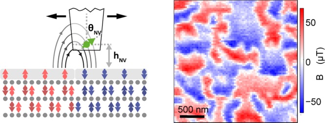
Antiferromagnets have recently emerged as attractive platforms for spintronics applications, offering fundamentally new functionalities compared with their ferromagnetic counterparts. Whereas nanoscale thin-film materials are key to the development of future antiferromagnetic spintronic technologies, existing experimental tools tend to suffer from low resolution or expensive and complex equipment requirements. We offer a simple, high-resolution alternative by addressing the ubiquitous surface magnetization of magnetoelectric antiferromagnets in a granular thin-film sample on the nanoscale using single-spin magnetometry in combination with spin-sensitive transport experiments. Specifically, we quantitatively image the evolution of individual nanoscale antiferromagnetic domains in 200 nm thin films of Cr2O3 in real space and across the paramagnet-to-antiferromagnet phase transition, finding an average domain size of 230 nm, several times larger than the average grain size in the film. These experiments allow us to discern key properties of the Cr2O3 thin film, including the boundary magnetic moment density, the variation of critical temperature throughout the film, the mechanism of domain formation, and the strength of exchange coupling between individual grains comprising the film. Our work offers novel insights into the magnetic ordering mechanism of Cr2O3 and firmly establishes single-spin magnetometry as a versatile and widely applicable tool for addressing antiferromagnetic thin films on the nanoscale.
Keywords: Antiferromagnets, magnetoelectrics, surface magnetization, intergranular exchange energy, nitrogen vacancy magnetometry, Hall magnetometry
Antiferromagnetic (AF) materials are abundant in nature, much more so than ferromagnets, but have been studied less thoroughly due to their insensitivity to magnetic fields and vanishing magnetization. Still, it has been widely recognized that faster and smaller spintronic devices require the use of purely AF, nanoscale, thin-film systems.1−8 The properties of such thin films deviate significantly from their bulk parents due to their morphology, which typically consists of closely packed grains. This granularity leads to the appearance of nanoscale domains with strongly pinned domain walls,6,8−10 a dramatic departure from the bulk case where domains are typically on the millimeter scale.13 Such behavior cannot be explained by a change of material properties such as magnetic anisotropy and exchange in the bulk volume. Instead, the influence of the surface becomes significant, namely, the boundary magnetism and the intergranular exchange coupling, dramatically changing the behavior of AFs. Imaging of domain structures for thin films is difficult. There exist a few techniques, including X-ray magnetic dichroism photoelectron emission microscopy (XML(C)D PEEM)11 as well as magnetic force microscopy (MFM),12 that are able to image thin-film domains, yet real-space imaging of magnetic domain nucleation and its influence on the electron transport response remains largely unexplored for thin-film AFs.
We present a consistent and quantitative study of these properties based on nanoscale nitrogen vacancy (NV) single-spin magnetic imaging14 and zero-offset anomalous Hall effect magnetometry (ZOHM)15 for a Cr2O3 thin film. This collinear magnetoelectric AF is highly relevant to AF spintronics,8 making it a showcase example of this combined approach. We image and study the formation of nanoscale domains across the paramagnet–AF phase transition with unprecedented signal-to-noise ratio and sub-100 nm spatial resolution, enabling a quantitative determination of the boundary magnetization. We find an average domain size of 230 nm, several times larger than the grain size of 50 nm in our film, indicating significant intergranular exchange coupling that dominates the magnetic alignment of neighboring grains. Furthermore, our ZOHM measurements allow us to determine the distribution of critical temperature across the grains of our film, enabling us to model the domain formation process and to confirm the strong intergranular exchange coupling.
Because of its room-temperature ordering and magnetoelectric switching capabilities,8,16,17 Cr2O3 is a key contender for future AF-based magnetoelectric memory devices. Breaking of the crystal bulk symmetry leads to the formation of a (0001) surface that consists of a layer of Cr atoms all belonging to the same AF sublattice. This surface termination presents a roughness-insensitive, out-of-plane surface magnetization on the order of few μB/nm2 (where μB is the Bohr magneton) whose orientation is rigidly linked to the AF order parameter16,18,19 (Figure 1b). Past work has shown that as the temperature approaches the critical temperature (Tcrit) the magnetization remains out-of-plane and is reduced in amplitude.20 This surface magnetization creates stray magnetic fields, which, in the far field, are quadrupolar in nature and decay with distance from the sample over length scales given by typical domain sizes or sample thickness.19,21,22 Exploiting such stray fields to address thin-film samples thus requires a sensitive magnetometer that can be brought in close proximity to the sample.
Figure 1.
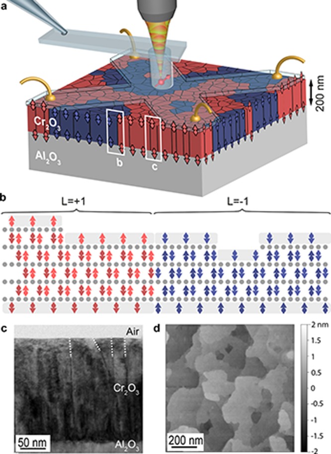
Schematic of experiment and thin-film antiferromagnetic sample. (a) Thin-film sample of antiferromagnetic Cr2O3 is examined using a combination of scanning single-spin magnetometry (red arrow) and zero-offset Hall magnetometry (light-blue cross with golden leads). (b) Cr2O3 is a bulk antiferromagnet with a roughness-insensitive, nonzero surface magnetization linked to the underlying order parameter, L. (c) Cross-sectional transmission electron microscopy image of the sample. The image shows the typical columnar grains comprising the Cr2O3 film (representative grain boundaries are highlighted by white dashed lines). (d) Atomic force microscopy of the Cr2O3 sample surface, showing atomically smooth terraces.
This nontrivial requirement is met by nanoscale, scanning NV magnetometry (Figure 1a),14,23,24 a versatile technique that has previously been used to study magnetism in ferromagnetic films25 and noncollinear antiferromagnets.26 The technique operates by scanning a single electronic spin in close vicinity to a surface to measure the magnetic field, BNV, along the fixed NV quantization axis through the Zeeman splitting of the NV’s optically detected electron spin resonance (see Supporting Information). It operates under ambient conditions and offers quantitative sensing, nanoscale imaging, and sensitivities sufficient to address individual electronic spins.27 These unique characteristics are ideally suited to address the nanoscale properties of pure AF systems, which lack an overall magnetic moment.
The samples we investigate consist of 200 nm thick Cr2O3 films grown on a c-cut sapphire substrate (see Supporting Information). The obtained film is granular with ∼50 nm sized columnar grains (Figure 1c) and very high crystallinity within each grain.28 The samples exhibit atomically smooth terraces bounded by 0.26 nm steps in topography, corresponding to single Cr–O3–Cr repetitions, as confirmed by atomic force microscopy (Figure 1d). For NV magnetometry, the sample is mounted on a Peltier element to control temperatures to within ±0.1 K during measurements. We prepare the film by heating it well above the AF-to-paramagnet transition (TNeel = 308 K in bulk12) and then cooling it back to the AF state in zero external magnetic field to induce a spontaneously formed pattern of AF domains.8
To investigate AF domains in the Cr2O3 film, we first use NV magnetometry to acquire a map of BNV at the Cr2O3 surface. In contrast with previous measurements of noncollinear AFs, where the measured stray field emerges from an overall ferrimagnetic moment due to the canting of the spins, in Cr2O3, NV magnetometry probes the stray field resulting from a single layer of uncompensated spins on the surface. The acquired stray field image then immediately confirms the presence of magnetic domains, as signaled by areas of positive or negative BNV, as shown in Figure 2a. Repeated scans of the same area show the same magnetic field pattern, indicating a minimal effect of the laser and microwave fields on the sample.28 As expected from a simplified picture of homogeneously magnetized domains with infinitely sharp domain walls,25 zeros in BNV indicate the locations of domain walls up to a small, constant shift, and broad maxima of BNV occur toward the boundaries of the domains. More quantitatively, we model this stray field by describing the magnetization m⃗ of the Cr2O3 film as two monolayers of out-of-plane polarized spins with moment density σz(x, y) and opposite orientations, separated by d = 200 nm (Figure 1b): m⃗(x, y, z) = σz(x, y)[δ(z) – δ(z + d)]ẑ, where δ is the Dirac delta function and ẑ is the out-of-plane unit vector. The measured stray magnetic field BNV can then be conveniently obtained by established methods of field propagation in Fourier space29,30
| 1 |
where TNV is a propagator that depends on the NV orientation (θNV, ϕNV) and the NV-to-sample distance, hNV (see Figure 2c). If hNV, θNV, and ϕNV are known, then eq 1 can be inverted and σz(x, y) directly obtained from the experimental data together with appropriate filtering.29 To determine these parameters, we developed an iterative, self-consistent method based on the data and our minimal model for Cr2O3’s surface magnetization described above. Using the resulting values hNV = 120 nm, θNV = 54°, and ϕNV = 92°, we reverse propagate the measured BNV(x, y) map to find σz(x, y), as shown in Figure 2b. This magnetization profile shows well-defined magnetic domains, with typical domain sizes ∼230 nm (determined by the peak width of the corresponding autocorrelation map), significantly larger than the 50 nm grain size in our film, indicating an intergranular exchange coupling that influences the order-parameter alignment of neighboring grains. At the same time, the very existence of domains and the small domain-wall feature size (on the scale of the grain size) suggest that strong pinning occurs at the grain boundaries during the cooling process. The reverse propagation also yields the average surface moment density of 2.14 ± 1.5 μB/nm2, as determined from a histogram of the inferred moment density map (Figure 2d). This represents the first measurement of the boundary magnetization of Cr2O3 at room temperature and is independently confirmed through additional measurements on a patterned thin-film Cr2O3 sample, which we prepared in a monodomain state by field cooling and on a patterned bulk, monodomain, single-crystal sample.28
Figure 2.
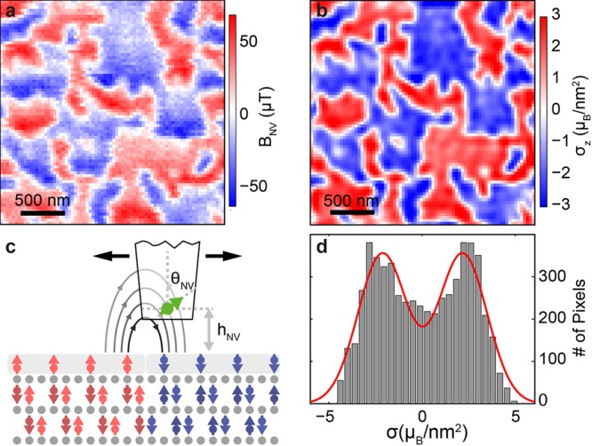
Domain imaging in antiferromagnetic Cr2O3. (a) Map of the measured stray magnetic field BNV above the Cr2O3 film and (b) the extracted moment density profile (see the main text) of the film, which reveals a domain pattern of spin-up and spin-down domains. (c) Measurement geometry and relevant experimental parameters for reverse propagation. (d) Histogram of surface moment density values found in panel b with a fit to a bimodal, Gaussian distribution (red), yielding an average moment density 2.14 ± 1.5 μB/nm2.
Further details of the nanoscale magnetic properties of our thin-film AF can be obtained by observing the temperature dependence of σz near the AF–paramagnet transition at the critical temperature of the thin film. We thus repeated moment density measurements for temperatures around TNeel and compared our findings to ZOHM measurements performed on a similarly prepared sample15 (Figure 3a). In brief, ZOHM measures the anomalous Hall resistance in a thin layer of Pt evaporated onto the Cr2O3 surface and is sensitive to the average Cr2O3 surface magnetic moment over the Hall cross area of ∼900 μm2. This method gives a precise readout of the averaged relative magnetization but does not provide spatial resolution or the magnitude of the moment density. The NV magnetometry data (Figure 3a) follow the temperature dependence of ZOHM and thereby allow us to calibrate the resulting Hall resistance to a quantitative magnetic moment density.
Figure 3.
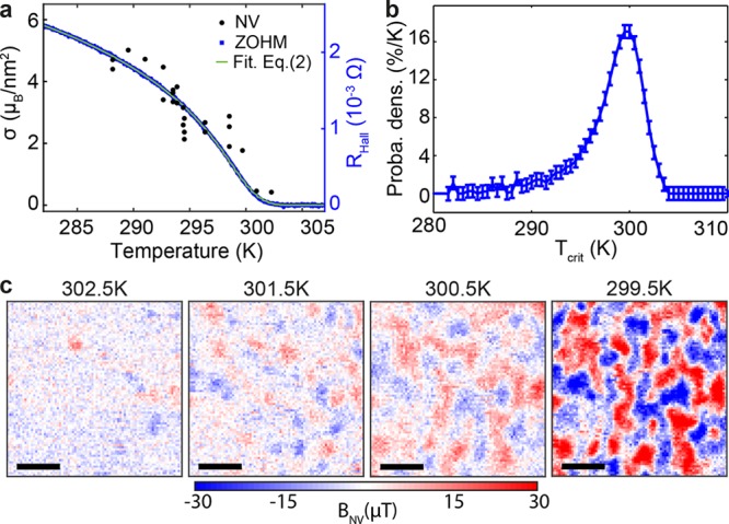
Spatial variation of critical temperatures. (a) Temperature dependence of moment density together with ZOHM data.15 The data are fitted (green) to a critical behavior with spatially varying critical temperatures (see eq 2 and the text for details). (b) Probability distribution of critical temperatures as determined from the fit in panel a. (c) Consecutive magnetic field maps obtained during cooling of the sample through the phase transition. Domains are nucleating at isolated spots and propagate laterally to form the domain pattern (scale bar: 500 nm).
The temperature dependence of σz determined by combining ZOHM and NV magnetometry (Figure 3a) shows a smooth tapering of σz through the phase transition, in contrast with the sharp drop to zero expected from the usually observed power-law dependence of σ(T) for magnetic phase transitions. Such behavior was previously attributed to spatial variations of Tcrit in thin films31,32 and can be readily accounted for by the convolution
| 2 |
where P(Tcrit) is the probability density for Tcrit and σ(τ) = σsat(1 – τ)β, with critical exponent, β, and saturation magnetization, σsat (σ(τ > 1) = 0). Fitting eq 2 to our data (green curve in Figure 3a) for fixed β = 0.35 allows us to extract P(Tcrit), as depicted in Figure 3b. The significant broadening of P(Tcrit) is evidence of the local inhomogeneity of Tcrit in the sample, which we assign to material defects such as twinning boundaries or lattice dislocations.8
The ability to measure fine spatial features of the magnetization pattern enables a detailed study of the paramagnetic-to-AF phase transition and the local variations in Tcrit at the level of individual domains. To directly observe these variations, we record snapshots of the stray field around Tcrit (Figure 3c). For the sample well above Tcrit, we detect no magnetic stray field exceeding our measurement noise, which indicates no surface magnetization and a paramagnetic phase. As the sample is cooled, spatially separated regions of nonzero magnetization spontaneously nucleate, but significant areas of the sample remain paramagnetic. Upon further cooling, this nucleation propagates until all areas of the sample show nonzero magnetization. This lateral spreading of AF domains with decreasing temperature is indicative of significant, intergranular exchange coupling. Without such coupling, each grain would nucleate independently and in a random fashion so that domains would typically be on the order of the grain size.
We developed a discrete model of the AF film28 based on our observations, taking into account inhomogeneities in Tcrit and the order parameter, σz. The discrete grains comprising the film are mutually exchange-coupled with a probability, PE, for the order parameter of neighboring grains to be locked by exchange (i.e., for exchange coupling exceeding thermal fluctuations). To test this interpretation, we also developed a differential field cooling (DFC) method (Figure 4a), which allows us to assess the efficiency of intergranular exchange coupling through ZOHM.33 We initialized the sample well above Tcrit and then applied a strong magnetic field in the +ẑ direction to provide an order-parameter selection stimulus8 toward an AF state with σz > 0 while the sample is cooled. At a temperature Tswitch, the magnetic field is reversed to yield a stimulus toward σz < 0, with which the sample is further cooled to 280 K. Finally, we measure the average order parameter ⟨σz(Tswitch)⟩ using ZOHM and determine the normalized magnetization L = ⟨σz(Tswitch)⟩/⟨σz(TRT)⟩ as a function of Tswitch (Figure 4b). We can use our model to understand the evolutions of L. For PE = 0, grains are independent, and their value of σz is determined by an applied order-parameter selection stimulus at the time of ordering, hence, L(Tswitch) = −1 + 2A(Tswitch), where A(Tswitch) = ∫Tswitch∞P(Tcrit) dTcrit is the unitless fractional sample area having Tcrit > Tswitch. For PE > 0, however, each grain will be influenced by its neighbors and we find L(Tswitch, PE) = −1 + 2A(Tswitch)ePE·(1–A(Tswitch)).28 A fit of L(Tswitch, PE) to the ZOHM data (Figure 4b) thus allows us to determine PE = 0.99, indicating that for our thin-film sample, intergranular exchange coupling largely dominates thermal fluctuations.
Figure 4.
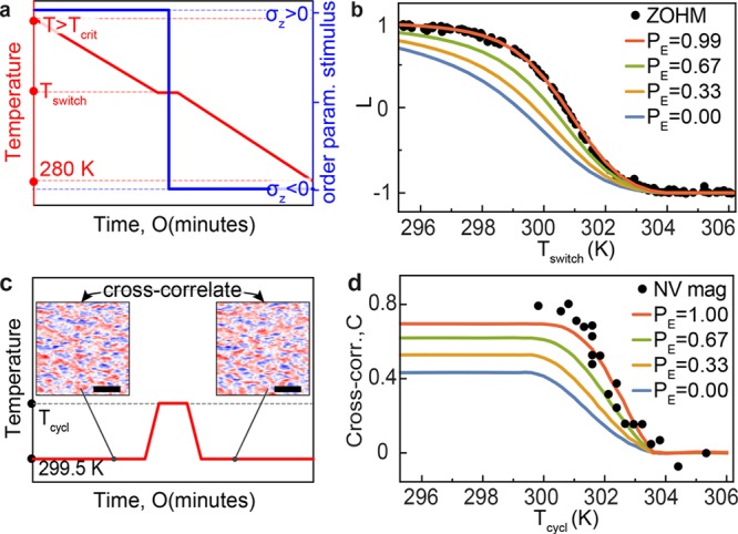
Determining intergranular exchange coupling. (a) Procedure for differential field cooling. The sample was cooled from a temperature T > Tcrit to T = Tswitch while applying a strong order-parameter selection stimulus (magnetic field) toward σz > 0. The stimulus was then inverted toward σz < 0, and the sample was further cooled to 280 K. (b) Average order parameter L = ⟨σz(Tswitch)⟩/⟨σz(TRT)⟩, measured by ZOHM, as a function of Tswitch. Data are fit to theory (see the text) using the probability distribution from Figure 3b and demonstrate significant intergranular exchange coupling PE ≈ 1. (c) Procedure for temperature cycling domain cross-correlation. The sample is imaged at Tstart = 299.5 K, subsequently heated to T = Tcycl, and cooled back to Tstart, where another image is taken (scale bar: 1 μm). (d) Cross-correlation between reference and sample image as a function of Tcycl, evidencing strong intergranular exchange coupling on the nanoscale.
Scanning NV magnetometry can also be used to quantitatively confirm such strong exchange coupling of neighboring grains on the level of individual AF domains. For this, we perform domain cross-correlation measurements under temperature cycling (Figure 4c). We record an AF domain image at an initial temperature Tstart = 299.5 K, subsequently set the sample temperature to Tcycl for ∼10 min, and finally cool the sample back to Tstart, where we record a second domain image. Specifically, the pixel-by-pixel correlation C(Tcycl) between reference and sample images (Figure 4d) measures the extent to which the domain pattern is preserved during heating. This procedure yields information closely related to DFC, all while avoiding experimental difficulties of applying and switching strong order-parameter stimuli (i.e., magnetic fields) in our imaging experiment. By analogy to DFC, we expect the correlation between grains to follow A(Tcycl) for PE = 0, whereas for PE > 0, we expect the domain pattern to be largely determined by high-Tcrit grains and the transition from correlated to uncorrelated to therefore be pushed to higher temperatures, as confirmed by granular thin-film simulations.28 A comparison of our correlation data (Figure 4d, black points) to the simulation (solid lines) provides further proof of the strong intergranular exchange coupling, which we obtain on the level of individual domains.
In this work, we have shown that the domain structure of thin-film AFs is largely determined by intergranular exchange coupling, without which domains would be limited to the size of individual grains. We have directly observed the nucleation process of the AF phase by real-space imaging and quantified important material properties of the film including the boundary magnetization and domain size. Furthermore, we correlated the emergent magnetotransport responses with the imaged AF domain pattern. Our results thus constitute an important step toward the general understanding of surface magnetization and domain formation in AFs as well as the appearance of magnetoelectricity in some families of insulating AFs, where confirmation of theories of monopolization strongly relies on the availability of reliable experimental data on boundary magnetization.34,35 These results are enabled by our versatile method for quantitative nanoscale imaging of AF order in thin-film materials, which uniquely combines two very different but equally powerful techniques: NV magnetometry and ZOHM. Our approach is largely complementary to the existing toolset for studying AF order, such as neutron36−38 or X-ray39−43 scattering as well as optical44 or scanning probe imaging,12 where combining high spatial resolution with high signal-to-noise ratio and quantitative imaging has remained elusive thus far. Although we have focused on Cr2O3, it is important to note that our approach is much more generally applicable. Previous studies using NV magnetometry have been successful in imaging noncollinear AFs26 that exhibit a ferrimagnetic moment, and here we have shown that also collinear, magnetoelectric AFs that exhibit boundary magnetization due to inversion symmetry breaking at the surface19,21 can be imaged. Furthermore, NV magnetometry is not limited to out-of-plane magnetization but is also sensitive to magnetic fields originating from in-plane moments. Thus NV magnetometry is applicable to a wide range of AFs as long as the resulting surface spin densities are within the NV magnetometry sensitivity limit, making it a valuable tool for nanoscale AF spintronics.
Acknowledgments
We thank Prof. O. G. Schmidt (IFW Dresden) for his insightful input in the initial stage of the project and S. Hoffman (Basel) and V. Jacques (CNRS Montpellier) for helpful discussions. We gratefully acknowledge financial support through the NCCR QSIT, a competence centre funded by the Swiss NSF, the SNI, and through SNF grant no. 143697 and 155845. This research has been partially funded by the European Commission’s 7th Framework Program (FP7/2007-2013) under grant agreement number 611143 (DIADEMS), the ERC within the EU Seventh Framework Programme (ERC grant no. 306277), and the EU FET Programme (FET open grant no. 618083).
Supporting Information Available
The Supporting Information is available free of charge on the ACS Publications website at DOI: 10.1021/acs.nanolett.8b04681.
Detailed method description for NV magnetometry and ZOHM, supporting experimental results, discussion of Cr2O3 surface termination, discussion of magnetic moment density determination, theoretical modeling of critical temperatures and granular ordering dynamics, and additional figures (ZIP)
Author Contributions
∥ P.A. and B.J.S. contributed equally.
The authors declare no competing financial interest.
Supplementary Material
References
- Sander D.; Valenzuela S. O.; Makarov D.; Marrows C. H.; Fullerton E. E.; Fischer P.; McCord J.; Vavassori P.; Mangin S.; Pirro P.; et al. The 2017 Magnetism Roadmap. J. Phys. D: Appl. Phys. 2017, 50, 363001. 10.1088/1361-6463/aa81a1. [DOI] [Google Scholar]
- Heron J. T.; Bosse J. L.; He Q.; Gao Y.; Trassin M.; Ye L.; Clarkson J. D.; Wang C.; Liu J.; Salahuddin S.; Ralph D. C.; Schlom D. G.; Iniguez J.; Huey B. D.; Ramesh R. Deterministic switching of ferromagnetism at room temperature using an electric field. Nature 2014, 516, 370–373. 10.1038/nature14004. [DOI] [PubMed] [Google Scholar]
- Jungwirth T.; Marti X.; Wadley P.; Wunderlich J. Antiferromagnetic spintronics. Nat. Nanotechnol. 2016, 11, 231–41. 10.1038/nnano.2016.18. [DOI] [PubMed] [Google Scholar]
- Baltz V.; Manchon A.; Tsoi M.; Moriyama T.; Ono T.; Tserkovnyak Y. Antiferromagnetic spintronics. Rev. Mod. Phys. 2018, 90, 015005 10.1103/RevModPhys.90.015005. [DOI] [Google Scholar]
- Seki S.; Ideue T.; Kubota M.; Kozuka Y.; Takagi R.; Nakamura M.; Kaneko Y.; Kawasaki M.; Tokura Y. Thermal Generation of Spin Current in an Antiferromagnet. Phys. Rev. Lett. 2015, 115, 266601. 10.1103/PhysRevLett.115.266601. [DOI] [PubMed] [Google Scholar]
- Wadley P.; Howells B.; Železnỳ J.; Andrews C.; Hills V.; Campion R. P.; Novak V.; Olejník K.; Maccherozzi F.; Dhesi S.; Martin S. Y.; Wagner T.; Wunderlich J.; Freimuth F.; Mokrousov Y.; Kuneš J.; Chauhan J. S.; Grzybowski M. J.; Rushforth A. W.; Edmonds K. W.; Gallagher B. L.; Jungwirth T. Electrical switching of an antiferromagnet. Science 2016, 351, 587–590. 10.1126/science.aab1031. [DOI] [PubMed] [Google Scholar]
- Loth S.; Baumann S.; Lutz C. P.; Eigler D. M.; Heinrich A. J. Bistability in atomic-scale antiferromagnets. Science 2012, 335, 196–199. 10.1126/science.1214131. [DOI] [PubMed] [Google Scholar]
- Kosub T.; Kopte M.; Hühne R.; Appel P.; Shields B.; Maletinsky P.; Hübner R.; Liedke M. O.; Fassbender J.; Schmidt O. G.; Makarov D. Purely antiferromagnetic magnetoelectric random access memory. Nat. Commun. 2017, 8, 13985. 10.1038/ncomms13985. [DOI] [PMC free article] [PubMed] [Google Scholar]
- Meinert M.; Graulich D.; Matalla-Wagner T. Electrical Switching of Antiferromagnetic Mn2Au and the Role of Thermal Activation. Phys. Rev. Appl. 2018, 9, 064040 10.1103/PhysRevApplied.9.064040. [DOI] [Google Scholar]
- O’Grady K.; Fernandez-Outon L. E.; Vallejo-Fernandez G. A new paradigm for exchange bias in polycrystalline thin films. J. Magn. Magn. Mater. 2010, 322, 883–899. 10.1016/j.jmmm.2009.12.011. [DOI] [Google Scholar]
- Grzybowski M. J.; Wadley P.; Edmonds K. W.; Beardsley R.; Hills V.; Campion R. P.; Gallagher B. L.; Chauhan J. S.; Novak V.; Jungwirth T.; Maccherozzi F.; Dhesi S. S. Imaging current-induced switching of antiferromagnetic domains in CuMnAs. Phys. Rev. Lett. 2017, 118, 057701 10.1103/PhysRevLett.118.057701. [DOI] [PubMed] [Google Scholar]
- Wu N.; He X.; Wysocki A. L.; Lanke U.; Komesu T.; Belashchenko K. D.; Binek C.; Dowben P. A. Imaging and Control of Surface Magnetization Domains in a Magnetoelectric Antiferromagnet. Phys. Rev. Lett. 2011, 106, 087202 10.1103/PhysRevLett.106.087202. [DOI] [PubMed] [Google Scholar]
- Fiebig M.; Fröhlich D.; Sluyterman v. L. G.; Pisarev R. V. Domain topography of antiferromagnetic Cr2O3 by second-harmonic generation. Appl. Phys. Lett. 1995, 66, 2906–2908. 10.1063/1.113699. [DOI] [Google Scholar]
- Maletinsky P.; Hong S.; Grinolds M. S.; Hausmann B.; Lukin M. D.; Walsworth R. L.; Loncar M.; Yacoby A. A robust scanning diamond sensor for nanoscale imaging with single nitrogen-vacancy centres. Nat. Nanotechnol. 2012, 7, 320–324. 10.1038/nnano.2012.50. [DOI] [PubMed] [Google Scholar]
- Kosub T.; Kopte M.; Radu F.; Schmidt O. G.; Makarov D. All-Electric Access to the Magnetic-Field-Invariant Magnetization of Antiferromagnets. Phys. Rev. Lett. 2015, 115, 097201 10.1103/PhysRevLett.115.097201. [DOI] [PubMed] [Google Scholar]
- He X.; Wang Y.; Wu N.; Caruso A. N.; Vescovo E.; Belashchenko K. D.; Dowben P. A.; Binek C. Robust isothermal electric control of exchange bias at room temperature. Nat. Mater. 2010, 9, 579–585. 10.1038/nmat2785. [DOI] [PubMed] [Google Scholar]
- Ashida T.; Oida M.; Shimomura N.; Nozaki T.; Shibata T.; Sahashi M. Observation of magnetoelectric effect in Cr2O3/Pt/Co thin film system. Appl. Phys. Lett. 2014, 104, 152409. 10.1063/1.4871515. [DOI] [Google Scholar]
- Belashchenko K. D. Equilibrium Magnetization at the Boundary of a Magnetoelectric Antiferromagnet. Phys. Rev. Lett. 2010, 105, 147204. 10.1103/PhysRevLett.105.147204. [DOI] [PubMed] [Google Scholar]
- Andreev A. F. Macroscopic magnetic fields of antiferromagnets. JETP Lett. 1996, 63, 758–762. 10.1134/1.566978. [DOI] [Google Scholar]
- Fallarino L.; Berger A.; Binek C. Giant temperature dependence of the spin reversal field in magnetoelectric chromia. Appl. Phys. Lett. 2014, 104, 022403 10.1063/1.4861780. [DOI] [Google Scholar]
- Dzyaloshinskii I. External magnetic fields of antiferromagnets. Solid State Commun. 1992, 82, 579–580. 10.1016/0038-1098(92)90236-3. [DOI] [Google Scholar]
- Astrov D. N.; Ermakov N. B.; Borovik-Romanov A. S.; Kolevatov E. G.; Nizhankovskii V. I. External quadrupole magnetic field of antiferromagnetic Cr2O3. JETP Lett. 1996, 63, 745–751. 10.1134/1.566976. [DOI] [Google Scholar]
- Appel P.; Neu E.; Ganzhorn M.; Barfuss A.; Batzer M.; Gratz M.; Tschöpe A.; Maletinsky P. Fabrication of all diamond scanning probes for nanoscale magnetometry. Rev. Sci. Instrum. 2016, 87, 063703 10.1063/1.4952953. [DOI] [PubMed] [Google Scholar]
- Rondin L.; Tetienne J.-P.; Hingant T.; Roch J.-F.; Maletinsky P.; Jacques V. Magnetometry with nitrogen-vacancy defects in diamond. Rep. Prog. Phys. 2014, 77, 056503. 10.1088/0034-4885/77/5/056503. [DOI] [PubMed] [Google Scholar]
- Tetienne J.-P.; Hingant T.; Martinez L.; Rohart S.; Thiaville A.; Diez L. H.; Garcia K.; Adam J.-P.; Kim J.-V.; Roch J.-F.; Miron I. M.; Gaudin G.; Vila L.; Ocker B.; Ravelosona D.; Jacques V. The nature of domain walls in ultrathin ferromagnets revealed by scanning nanomagnetometry. Nat. Commun. 2015, 6, 6733. 10.1038/ncomms7733. [DOI] [PubMed] [Google Scholar]
- Gross I.; Akhtar W.; Garcia V.; Martínez J.; Chouaieb S.; Garcia K.; Carrétéro C.; Barthélémy A.; Appel P.; Maletinsky P.; Kim J.-V.; Chauleau J. Y.; Jaouen N.; Viret M.; Bibes M.; Fusil S.; Jacques V. Real-space imaging of non-collinear antiferromagnetic order with a single-spin magnetometer. Nature 2017, 549, 252–256. 10.1038/nature23656. [DOI] [PubMed] [Google Scholar]
- Grinolds M. S.; Hong S.; Maletinsky P.; Luan L.; Lukin M. D.; Walsworth R. L.; Yacoby A. Nanoscale magnetic imaging of a single electron spin under ambient conditions. Nat. Phys. 2013, 9, 215–219. 10.1038/nphys2543. [DOI] [Google Scholar]
- See the Supporting Information for information regarding the implementation of NV magnetometry and ZOHM, sample preparation, a detailed description of the determination of the magnetic moment density, determination of P(Tcrit), and modeling of granular ordering dynamics in the film.
- Meyer E.; Hug H. J.; Bennewitz R.. Scanning Probe Microscopy; Springer-Verlag: Berlin Heidelberg, 2004; 10.1007/978-3-662-09801-1. [DOI] [Google Scholar]
- Roth B. J.; Sepulveda N. G.; Wikswo J. P. Using a magnetometer to image a two-dimensional current distribution. J. Appl. Phys. 1989, 65, 361–372. 10.1063/1.342549. [DOI] [Google Scholar]
- Fallarino L.; Berger A.; Binek C. Magnetic field induced switching of the antiferromagnetic order parameter in thin films of magnetoelectric chromia. Phys. Rev. B: Condens. Matter Mater. Phys. 2015, 91, 054414 10.1103/PhysRevB.91.054414. [DOI] [Google Scholar]
- Al-Mahdawi M.; Shiokawa Y.; Pati S. P.; Ye S.; Nozaki T.; Sahashi M. Apparent critical behaviour of sputter-deposited magnetoelectric antiferromagnetic Cr2O3 films near Néel temperature. J. Phys. D: Appl. Phys. 2017, 50, 155004. 10.1088/1361-6463/aa623e. [DOI] [Google Scholar]
- Kosub T.Ferromagnet-Free Magnetoelectric Thin Film Elements. Ph.D. thesis, Technischen Universität Chemnitz, 2017. [Google Scholar]
- Thöle F.; Fechner M.; Spaldin N. A. First-principles calculation of the bulk magnetoelectric monopole density: Berry phase and Wannier function approaches. Phys. Rev. B: Condens. Matter Mater. Phys. 2016, 93, 195167. 10.1103/PhysRevB.93.195167. [DOI] [Google Scholar]
- Meier Q. N.; Fechner M.; Nozaki T.; Sahashi M.; Salman Z.; Prokscha T.; Suter A.; Schoenherr P.; Lilienblum M.; Borisov P.; Dzyaloshinskii I. E.; Fiebig M.; Luetkens H.; Spaldin N. A. Search for the magnetic monopole at a magnetoelectric surface. Phys. Rev. X 2019, 9, 011011 10.1103/PhysRevX.9.011011. [DOI] [Google Scholar]
- Shull C. G.; Smart J. S. Detection of Antiferromagnetism by Neutron Diffraction. Phys. Rev. 1949, 76, 1256–1257. 10.1103/PhysRev.76.1256.2. [DOI] [Google Scholar]
- Sosnowska I.; Neumaier T. P.; Steichele E. Spiral magnetic ordering in bismuth ferrite. J. Phys. C: Solid State Phys. 1982, 15, 4835–4846. 10.1088/0022-3719/15/23/020. [DOI] [Google Scholar]
- Schreyer A.; Schmitte T.; Siebrecht R.; Bödeker P.; Zabel H.; Lee S. H.; Erwin R. W.; Majkrzak C. F.; Kwo J.; Hong M. Neutron scattering on magnetic thin films: Pushing the limits (invited). J. Appl. Phys. 2000, 87, 5443–5448. 10.1063/1.373367. [DOI] [Google Scholar]
- Nolting F.; Scholl A.; Stohr J.; Seo J. W.; Fompeyrine J.; Siegwart H.; Locquet J. P.; Anders S.; Luning J.; Fullerton E. E.; Toney M. F.; Scheinfein M. R.; Padmore H. A. Direct observation of the alignment of ferromagnetic spins by antiferromagnetic spins. Nature 2000, 405, 767–769. 10.1038/35015515. [DOI] [PubMed] [Google Scholar]
- Alders D.; Tjeng L. H.; Voogt F. C.; Hibma T.; Sawatzky G. A.; Chen C. T.; Vogel J.; Sacchi M.; Iacobucci S. Temperature and thickness dependence of magnetic moments in NiO epitaxial films. Phys. Rev. B: Condens. Matter Mater. Phys. 1998, 57, 11623–11631. 10.1103/PhysRevB.57.11623. [DOI] [Google Scholar]
- Kuiper P.; Searle B. G.; Rudolf P.; Tjeng L. H.; Chen C. T. X-ray magnetic dichroism of antiferromagnet Fe2O3: The orientation of magnetic moments observed by Fe 2p x-ray absorption spectroscopy. Phys. Rev. Lett. 1993, 70, 1549–1552. 10.1103/PhysRevLett.70.1549. [DOI] [PubMed] [Google Scholar]
- Mertins H.-C.; Oppeneer P. M.; Kuneš J.; Gaupp A.; Abramsohn D.; Schäfers F. Observation of the X-Ray Magneto-Optical Voigt Effect. Phys. Rev. Lett. 2001, 87, 047401 10.1103/PhysRevLett.87.047401. [DOI] [PubMed] [Google Scholar]
- Valencia S.; Kleibert A.; Gaupp A.; Rusz J.; Legut D.; Bansmann J.; Gudat W.; Oppeneer P. M. Quadratic X-Ray Magneto-Optical Effect upon Reflection in a Near-Normal-Incidence Configuration at the M Edges of 3d-Transition Metals. Phys. Rev. Lett. 2010, 104, 187401. 10.1103/PhysRevLett.104.187401. [DOI] [PubMed] [Google Scholar]
- Saidl V.; Němec P.; Wadley P.; Hills V.; Campion R. P.; Novák V.; Edmonds K. W.; Maccherozzi F.; Dhesi S. S.; Gallagher B. L.; Trojánek F.; Kuneš J.; Železný J.; Malý P.; Jungwirth T. Optical determination of the Néel vector in a CuMnAs thin-film antiferromagnet. Nat. Photonics 2017, 11, 91–96. 10.1038/nphoton.2016.255. [DOI] [Google Scholar]
Associated Data
This section collects any data citations, data availability statements, or supplementary materials included in this article.


