

Abstract
2D vertical van der Waals (vdW) heterostructures with atomically sharp interfaces have attracted tremendous interest in 2D photonic and optoelectronic applications. Band alignment engineering in 2D heterostructures provides a perfect platform for tailoring interfacial charge transfer behaviors, from which desired optical and optoelectronic features can be realized. Here, by developing a two‐step chemical vapor deposition strategy, direct vapor growth of monolayer PbI2 on monolayer transition metal dichalcogenides (TMDCs) (WS2, WSe2, or alloying WS2(1− x )Se2 x), forming bilayer vertical heterostructures, is demonstrated. Based on the calculated electron band structures, the interfacial band alignments of the obtained heterostructures can be gradually tuned from type‐I (PbI2/WS2) to type‐II (PbI2/WSe2). Steady‐state photoluminescence (PL) and time‐resolved PL measurements reveal that the PL emissions from the bottom TMDC layers can be modulated from apparently enhanced (for WS2) to greatly quenched (for WSe2) compared to their monolayer counterparts, which can be attributed to the band alignment–induced distinct interfacial charge transfer behaviors. The band alignment nature of the heterostructures is further demonstrated by the PL excitation spectroscopy and interlayer exciton investigation. The realization of 2D vertical heterostructures with tunable band alignments will provide a new material platform for designing and constructing multifunctional optoelectronic devices.
Keywords: band alignments, charge transfers, photoluminescence enhancement, photoluminescence quenching, van der Waals heterostructures
Energy band alignment engineering at the interface of semiconductor heterostructure is crucial for tuning its optical and electronic properties and realizing new functional photonic and optoelectronic devices.1, 2, 3, 4, 5, 6, 7, 8 Compared to conventional semiconductor heterostructures, the emerging 2D layered heterostructures with van der Waals (vdW) interaction between the layers offer a perfect platform for band alignment engineering via stacking different layers with distinct band structures.9, 10 In addition, the formed atomically sharp interfaces in these heterostructures facilitate many interfacial photophysics processes, such as interfacial charge transfer,11, 12, 13, 14 which can be utilized for high‐performance device applications. For 2D layered heterostructures with a type‐II (staggered) band alignment, photogenerated electrons or holes can transfer across the interface and be separated at different layers due to the band offset, making these heterostructures ideal for light harvesting and photodetection.15, 16, 17 In contrast, with a type‐I (straddling) band alignment, the photogenerated electrons and holes in the wider bandgap layer can efficiently transfer into the layer with a narrower bandgap, leading to an increased carrier population and enhanced photoluminescence emission, which has the potential for light‐emitting applications.18, 19, 20
Monolayer transition metal dichalcogenides (TMDCs) with direct bandgap covering a wide energy range are ideal candidates for preparing the 2D layered heterostructures.21, 22, 23 However, due to the band structures, it is difficult to form type‐I band alignment from typical TMDCs. Although the band alignment of 2D layered heterostructure can be influenced by introducing an external electric field or mechanical field,24, 25 the small tunability and poor controllability largely prevent these methods from practical applications. In contrast, by carefully selecting the layered materials, the engineering of band structure configurations and even the tuning of the type of the band alignments, e.g., the transition from type‐II to type‐I, in heterostructures can be realized. To this end, monolayer lead iodide (PbI2) with a wider bandgap and higher light absorption coefficient26, 27, 28 provides the possibility of forming vdW heterostructures with monolayer TMDCs for different band alignments. Furthermore, the 2D vdW heterostructure with a large‐range tunable band alignment can be obtained by introducing the alloying TMDCs.29, 30, 31, 32, 33, 34
Here, we demonstrate, for the first time, a direct vapor phase growth of vdW heterostructures composed of monolayer PbI2 and monolayer alloying WS2(1− x )Se2 x (0 ≤ x ≤ 1) through a two‐step chemical vapor deposition (CVD) strategy. By tuning different x values in the bottom alloying TMDC monolayers, the band alignment of these heterostructures emerges a transition from type‐I (PbI2/WS2, x = 0) to type‐II (PbI2/WSe2, x = 1), with a transition point at x = 0.67 (PbI2/WS0.67Se1.33). Meanwhile, the photoluminescence (PL) emission from the bottom TMDC layers can also be modulated from apparently enhanced (for WS2) to greatly quenched (for WSe2) compared to their pristine monolayer counterparts, which can be attributed to the band alignment–induced distinct interfacial charge transfer behaviors. We further demonstrate the type‐I and type‐II band alignment nature of the PbI2/WS2 and PbI2/WSe2 heterostructures by photoluminescence excitation (PLE) spectroscopy and the study of interlayer exciton (I‐exciton) behaviors, respectively. These 2D layered heterostructures with engineered band alignment not only provide a platform for fundamental physical investigations but also have potential applications in integrated electronic and optoelectronic applications.
PbI2/TMDC vertical heterostructures were synthesized via a two‐step CVD strategy (Figure 1 a). At first, the bottom TMDC (WS2, WSe2, or the alloying WS2(1− x )Se2 x) monolayers were grown with the same method described in our previous works.29, 33, 34 Briefly, a quartz boat loaded with the WS2, WSe2, or the mixed powders was placed at the heating zone while a substrate (Si/300 nm SiO2) was placed at the downstream region of a tube furnace. The furnace was then stably heated to 1050 °C within 40 min and maintained at this temperature for 5 min, with the Ar gas flow at a rate of 50 sccm for transporting the source to the substrate. The alloying WS2(1− x )Se2 x monolayers with the desired x value can be obtained by adjusting the mass ratio between the WS2 and WSe2 powders (see Figure S1 in the Supporting Information). In the second step, the substrate with as‐grown TMDC monolayers was rapidly transferred to the downstream of the other furnace with a quartz boat loaded with PbI2 powder placed at the heating zone. The furnace was then heated to 400 °C within 30 min and maintained at this temperature for 20 min with the Ar gas flow at a rate of 30 sccm. During the growth, PbI2 prefers to crystallize on the as‐grown TMDCs to form heterostructures instead of forming monolayers on the substrate, probably due to a higher absorption energy of TMDCs compared to the that with the substrate.35 By varying the deposition position (relating to the deposition temperature) of the substrate in the second step, the thickness of PbI2 can be controlled in general and the heterostructures comprising of monolayer WS2 and monolayer PbI2 were obtained. Since the PbI2 layers were grown at such a low temperature, the bottom TMDC monolayers were prevented from thermal damage during the formation of heterostructures.
Figure 1.
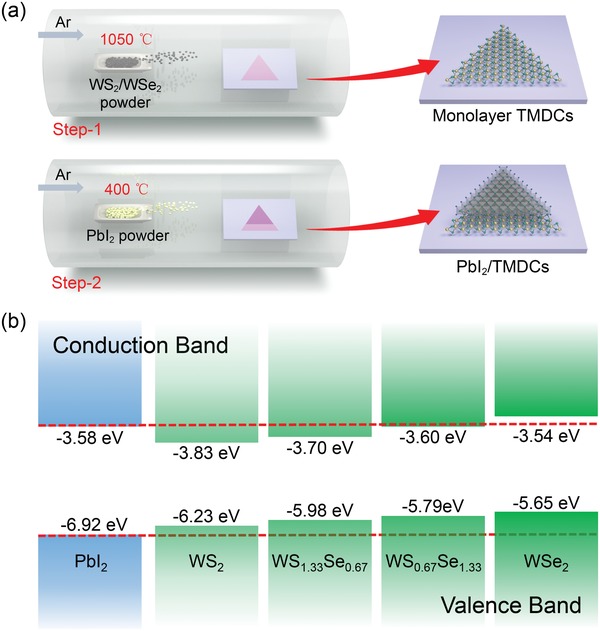
a) Illustration of the two‐step CVD strategy for the growth of PbI2/TMDC heterostructure. TMDCs (WS2, WSe2, or alloying WS2(1− x )Se2 x). b) Calculated energy band structures of monolayer PbI2, monolayer WS2(1− x )Se2 x (x = 0, 0.33, 0.67, and 1). Red dash lines indicate the CBM and VBM of PbI2. These band structures suggest a possible band alignment transition from type‐I (PbI2/WS2) to type‐II (PbI2/WSe2).
On the basis of ab initio simulation calculations (HSE06) of the electronic band structure of WS2, WSe2, alloying WS2(1− x )Se2 x and PbI2, the band alignments of PbI2/WS2 and PbI2/WSe2 show straddling and staggered configurations (Figure 1b; see the “Experimental Section” for detail), respectively. Thus, type‐I and type‐II vdW heterostructures with distinct optical and electronic properties can be realized by constructing monolayer PbI2 with monolayer WS2 and WSe2, respectively. In addition, for the WS2(1− x )Se2 x, with the x value varying from 0 to 1, both the conduction band minimum (CBM) and the valence band maximum (VBM) would become higher while the bandgap is smaller, which agrees with the previous reports.33, 36 Therefore, the band alignment of the heterostructures can be dynamically engineered from type‐I to type‐II by controlling the x value of the bottom WS2(1− x )Se2 x monolayer and a transition point can be found with a certain x value at which the CBM of WS2(1− x )Se2 x is equal to that of PbI2. This indicates that the charge transfer behaviors at the interface can be largely controlled by tuning the sign and amplitude of the band offset between the PbI2 and TMDCs in heterostructures.
To reveal the growth process of the top PbI2 monolayer on the bottom TMDCs, we took the PbI2/WS2 heterostructure as an example and recorded optical images of the heterostructures obtained with typical growth time varying from 0 to 20 min (Figure 2 a). The PbI2 was found to grow initially at the edge of WS2, where there are probably more dangling bonds and defects.37 Then, the PbI2 epitaxially grows across the WS2 surface, forming the PbI2/WS2 heterostructure. Given a long growth time, a whole covering of the top PbI2 on WS2 can be achieved. Figure 2b shows the atomic force microscope (AFM) images of typical areas marked with rectangles in an optical image of the 10 min growth sample (Figure 2a). AFM line profiles shown as insets in Figure 2b clearly demonstrate the formation of monolayer–monolayer heterostructure, with the height of uncovered WS2 being 0.7 nm and the heterostructure being 1.4 nm (PbI2 layer 0.7 nm).38, 39 High‐resolution transmission electron microscope (HRTEM) image of the heterostructure is shown in Figure 2c. Distinct Moiré patterns caused by the overlapping lattices of the PbI2 and WS2 were observed, demonstrating the formation of PbI2/WS2 vertical heterostructure as well. Fast Fourier transform (FFT) of this HRTEM image (Figure 2d) shows two sets of hexagonally arranged diffraction patterns, which can be assigned the [100] plane of PbI2 (yellow circles, 0.38 nm lattice spacing) and WS2 (red circles, 0.27 nm lattice spacing),33, 39 respectively. This large lattice mismatch (40.7%) between the PbI2 and WS2 indicates the ultrahigh tolerance of lattice mismatch in vdW heterostructure. Additional characterization of PbI2/WS2 heterostructure is provided by cross‐sectional TEM (Figure 2e), which directly gives the evidence of the stacking of the PbI2 above WS2. Meanwhile, corresponding elemental energy dispersive X‐ray spectroscopy (EDS) results of the cross section also confirm the existence of PbI2 and WS2 in the heterostructure (see Figure S2 in the Supporting Information).
Figure 2.
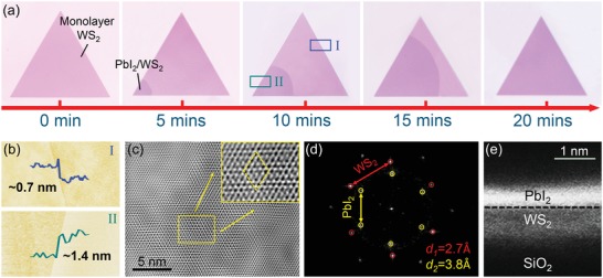
a) Optical images of the PbI2/WS2 obtained at different growth time. b) AFM images obtained at areas I (blue rectangle) and II (green rectangle) of the 10 min growth sample shown in (a). c) HRTEM image taken from the heterostructure, indicating the vertically stacked PbI2 and WS2 layers with the Moiré pattern. Scale bar: 5 nm. Inset: amplifying image from the yellow rectangle and the yellow dash rhombus indicates the periodicity of the Moiré pattern. d) FFT of the HRTEM image in panel (c). The hexagonally arranged diffraction patterns of PbI2 and WS2 are shown with yellow and red circles, respectively. The lattice spaces are marked. e) Bright‐field TEM image of the cross‐sectional morphology of PbI2/WS2 heterostructure. Scale bar: 1 nm.
In order to demonstrate the band alignment and the charge transfer behaviors, we choose three typical heterostructures, PbI2/WS2, PbI2/WS0.67Se1.33, and PbI2/WSe2. The optical images of these heterostructures with half‐covered PbI2 are shown in Figure 3 a–c. We observed clear optical contrast between these heterostructures and the bottom monolayers. Typical height profiles recorded from the AFM measurements are shown as insets in Figure 3a–c, indicating the formation of monolayer–monolayer heterostructures. Micro‐Raman spectroscopy was used to further characterize the heterostructures. For all spectra recorded at heterostructures, the vibrational modes of PbI2, containing Eg (75.3 cm−1), A1g (95.5 cm−1), and A2u (113.1 cm−1), were observed with relative weak intensity (Figure 3d–f), which agrees with the literature.28 Typical Raman peaks of A1g(S–W) (417.9 cm−1) and E2g (351.9 cm−1) from WS2 and A1g(Se–W) (250.0 cm−1) from WSe2 were observed in PbI2/WS2 and PbI2/WSe2 heterostructures. The Raman spectrum of PbI2/WS0.67Se1.33 heterostructure shows additional vibrational modes of E2g(S–W) − LA(S–W) + A1g(Se–W) − LA(Se–W) (a mode) and A1g(S–W–Se) (b mode) compared to WS2 and WSe2, demonstrating the formation of alloying layer. We noted that the Raman vibrational modes of TMDCs in heterostructures all show slight blueshifts compared to the monolayer counterparts, which is probably due to the strain effect induced by the top PbI2 layer.
Figure 3.
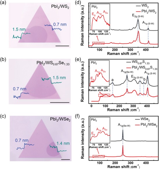
a–c) Optical images and d–f) Raman spectra of PbI2/WS2, PbI2/WS0.67Se1.33, and PbI2/WSe2 heterostructures. The Raman vibrational modes are labeled in the spectra. The peak a and peak b in panel (e) represent the E2g(S–W) − LA(S–W) + A1g(Se–W) − LA(Se–W) and A1g(S–W–Se) modes, respectively. Dash lines are used to guide the peak positions.
Steady‐state PL spectroscopy, PL mapping, and the time‐resolved photoluminescence (TRPL) spectroscopy were performed to study the PL emission intensity and dynamics of the bottom TMDC layer in these heterostructures, which can reflect the band alignment–induced interfacial charge transfer behaviors at the interface. The PL intensity mapping (at the emission wavelength of the bottom TMDCs) of PbI2/WS2, PbI2/WS0.67Se1.33, and PbI2/WSe2 heterostructures is shown in Figure 4 a1–a3, respectively. Typical PL spectra collected in the heterostructures and the bare monolayers are compared in Figure 4b1–b3. We observed that the PL intensity of WS2 is significantly enhanced in PbI2/WS2 heterostructure compared to that in monolayer WS2. In contrast, the WSe2 PL in the PbI2/WSe2 heterostructure shows strong intensity quenching. Only a slight enhancement of the WS0.67Se1.33 PL was observed in the PbI2/WS0.67Se1.33 heterostructure. The PL enhancing or quenching of TMDCs in their corresponding heterostructures can be quantified by defining an enhancing factor of α = I H/I M, where I H and I M are the PL intensity of TMDCs in heterostructure and monolayer, respectively. The α values of ≈2.02, 1.12, and 0.09 were obtained in PbI2/WS2, PbI2/WS0.67Se1.33, and PbI2/WSe2, respectively, clearly demonstrating the transition from PL enhancement to PL quenching. In addition, we noted that the PL of the bottom monolayer all shows an obvious redshifted peak (≈32 meV in PbI2/WS2, ≈22 meV in PbI2/WS0.67Se1.33, and ≈21 meV in PbI2/WSe2) in the heterostructure, which suggests a strong interlayer coupling between the PbI2 and bottom layers.40 TRPL spectroscopy was performed to study the PL dynamics in these heterostructures (Figure 4c1–c3). For both PbI2/WS2 and PbI2/WS0.67Se1.33, the PL decay curves of the TMDCs in monolayer and heterostructures are quite similar, with only a slight shift to longer time in PbI2/WS2. In contrast, the lifetime of WSe2 PL is dramatically decreased in PbI2/WSe2 heterostructure compared to the monolayer, implying an additional carrier decay channel of the WSe2 being created in the heterostructure.
Figure 4.
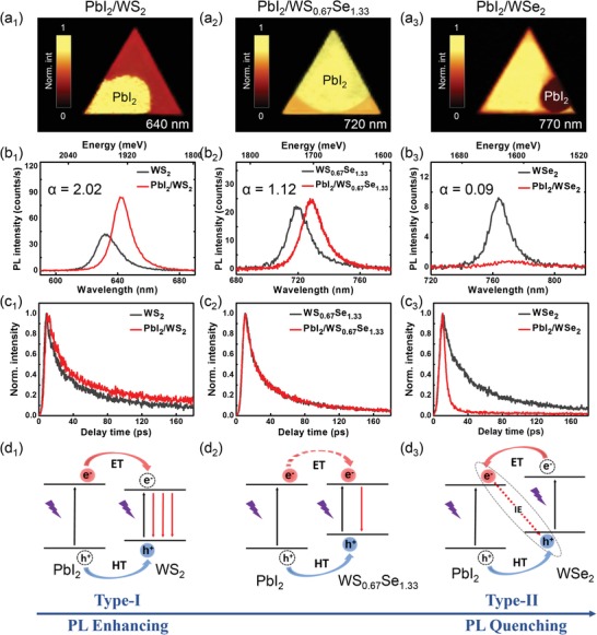
a1–a3) 2D PL mapping, b1–b3) typical PL spectra, and c1–c3) TRPL of TMDCs in PbI2/WS2, PbI2/WS0.67Se1.33, and PbI2/WSe2 heterostructures. The PbI2‐covered regions are marked. Values of enhancing factor α are marked. d1–d3) Schematic of the charge transfer processes in PbI2/WS2, PbI2/WS0.67Se1.33, and PbI2/WSe2 heterostructures. The black straight arrow represents the excitation while the red straight arrow represents the direct recombination. The red dash arrow represents the indirect interlayer recombination. ET: electron transfer, HT: hole transfer.
The observed different PL behaviors in different heterostructures can be well interpreted by the band alignment–induced charge transfer processes. For PbI2/WS2 heterostructure with type‐I band alignment, upon laser excitation, both the hole and electron can transfer from the PbI2 to the WS2 layer, leading to an increased carrier population and thus enhanced WS2 PL. In addition, the transfer time between the PbI2 and WS2 layer should be at very short time scale, and these transferred carriers should recombine through the same channel of the carriers which generated in WS2 layer, resulting in the mostly unchanged PL decay curve. For PbI2/WS0.67Se1.33 heterostructure, the CBM of WS0.67Se1.33 is roughly equal to that of PbI2 monolayer, which leads to the suppression of the electron transfer from PbI2 to WS2. Therefore, we did not observe a large enhancement of the PL like in the PbI2/WS2 heterostructure. For PbI2/WSe2 heterostructure with type‐II band alignment, the photogenerated electron and hole are, respectively, separated into PbI2 and WSe2 layers after charge transfer, leading to the extra decay channel for the electrons and thereby resulting the quenching of the WSe2 PL.
We further performed PLE experiments to experimentally demonstrate the type‐I band alignment nature of PbI2/WS2 heterostructure. The PL enhancement factor α as a function of excitation laser wavelength is shown in Figure 5 a. A rapid decrease of α value from ≈2 to ≈1 was observed in the excitation wavelength range of 510–550 nm, which matches the absorption edge of PbI2 as reported in the previous work.28 Within the range of 400–510 nm, both the PbI2 and WS2 layers were excited, where photogenerated carriers in PbI2 can be injected into the WS2. However, for excitation wavelength longer than 550 nm, only the WS2 layer was excited without external carrier injection so that the WS2 PL intensity in heterostructure equals to that of the monolayer WS2. The PLE experiment corroborated that the PL enhancement of WS2 originates from the charge transfer of PbI2, demonstrating the type‐I band alignment of PbI2/WS2 heterostructure. For PbI2/WSe2 heterostructure with type‐II alignment, the I‐excitons were observed and characterized. The PL spectrum collected from the PbI2/WSe2 heterostructure with a long integration time is depicted in Figure 5b. The whole spectral profile can be fitted by two Lorentzian peaks, the positions of which are located at 774.4 and 800.4 nm, respectively. We attribute the 774.4 and 800.4 nm peaks to the A‐exciton of WSe2 and I‐exciton, respectively. The experimentally observed energy difference between the A‐exciton and I‐exciton is 52 meV, which agrees with the energy difference between the CBM of WSe2 and PbI2 obtained from theoretical calculation (Figure 1b). We also performed TRPL measurement on the I‐exciton and observed an additional ultralong lifetime of 642 ps at 800.4 nm, which is consistent with the indirect nature of the I‐exciton (Figure 5c).41
Figure 5.
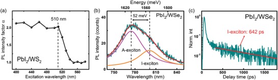
a) PL enhancement factor α as a function of excitation laser wavelength. b) PL spectrum collected from the PbI2/WSe2 heterostructure. c) TRPL curve of the I‐exciton at 800.4 nm showing an additional ultralong lifetime with a value of 642 ps. The fast decay originates from the A‐excitons which are spectrally overlapped at this wavelength.
In summary, we have theoretically and experimentally demonstrated the band alignment engineering of direct vapor growth 2D vdW heterostructures, which consist of monolayer PbI2 and monolayer TMDCs such as WS2, WSe2, and the alloying WS2(1− x )Se2 x. These heterostructures were characterized by AFM, TEM, Raman spectroscopy, steady‐state spectroscopy, and TRPL spectroscopy. The obtained PbI2/WS2 heterostructure has the type‐I band alignment with enhanced WS2 PL emission compared to the monolayer, which agrees well with the charge transfer behavior in type‐I heterostructure. In contrast, PbI2/WSe2 heterostructure with the type‐II band alignment shows quenched WSe2 PL and much shorter PL lifetime, which is due to the band alignment–induced extra carrier decay channel and the separation of electrons and holes in different layers. In addition, interlayer excitons with much longer lifetime have also been observed in these type‐II heterostructures. We have further shown that the band alignment can be precisely tuned by introducing the WS2(1− x )Se2 x alloying monolayer to prepare PbI2/WS2(1− x )Se2 x heterostructures. Our work offers important guidance for preparing 2D vdW heterostructures with desirable band alignment, potentially leading to the realization of functional 2D photonic and optoelectronic devices.
Experimental Section
Density Functional Theory Calculation: Density functional (DF) theory calculations were performed using the generalized gradient approximation for the exchange‐correlation potential, the projector augmented wave method, and a plane‐wave basis set as implemented in the Vienna ab initio simulation package (VASP).42, 43 van der Waals forces were considered at the self‐consistent vdW–DF level, which includes of a nonlocal correlation functional and an exchange functional in the optB86b form (optB86b–vdW).44, 45 This functional allows the accurate description of the structural properties of layered heterostructures.46, 47, 48 Electronic structures were calculated using the hybrid HSE06 functionals.49 Kinetic energy cutoffs of 500 and 400 eV for the plane‐wave basis sets were adopted for geometric and electronic structural calculations of the unit and super cells, respectively. A unit cell was used to model WSe2, WS2, and PbI2 monolayers while a 3 × 3 × 1 supercell was employed to model WS2 xSe2(1− x ) alloys. Two k‐meshes of 9 × 9 × 1 and 3 × 3 × 1 were adopted to sample the first Brillouin zones of the unit and super cells, respectively. A vacuum layer of 15 Å was used to eliminate the image interactions from adjacent unit cells along the normal layer direction. The cell shape and volume of all configurations and all atomic positions were fully relaxed until the residual force per atom was less than 0.01 eV Å−1. The band edges were aligned using the vacuum level.
Two ordered substitution models were used for considering the WS0.67Se1.33 and WS1.33Se0.67 alloys, as shown in Figure S3 (Supporting Information). Such an ordered substitution model substantially reduces computational costs and complicity, which was found to be able to offer good consistency with models fully considering disorders.50 All the S atoms and Se atoms were evenly distributed on both sides. Calculations were performed at the Physics Lab of High‐Performance Computing of Renmin University of China and the Shanghai Supercomputer Center.
Characterizations of As‐Grown PbI2/TMDC Heterostructures: AFM measurements were in situ performed with a Bruker Dimension ICON AFM with Pt/Ir‐coated tips (ACCESS EFM). For TEM characterizations, the WS2 monolayers were first transferred onto a grid through a polymethyl methacrylate (PMMA)‐assisted positioning transfer method. Monolayers on SiO2/Si wafer were coated with PMMA (950 K, A3) via spin‐coating at a speed of 2000 rpm for 1 min, and then maintained 2 h for baking the wafer at 180 °C. After immersing into the KOH (15 m) solution for 12 h, the PMMA film was taken out from the KOH solution and swilled fully with deionized water. The cleaned PMMA film was then removed onto a grid of copper, and this grid was exposed to acetone vapor at 40 °C in the atmosphere for the PMMA removing. Finally, the target WS2 monolayers on the grid of copper were obtained for the step‐2 growth process to form PbI2/WS2 heterostructures on grid which can be used for the TEM characterizations.
Micro‐Raman Spectra and Steady‐State PL Spectra Measurements: Micro‐Raman spectra were measured using a confocal microscope (WITec, alpha‐300) with a 532 nm diode continuous‐wave laser as the excitation. The laser beam was focused on the sample with a spot diameter of ≈800 nm from the top by an objective lens (50×, Zeiss, 0.75 NA), while Raman signal was collected by the same objective lens. Steady‐state PL spectra were measured using the same confocal microscope but with 405 nm continuous‐wave laser as the excitation.
TRPL Experiments: TRPL experiments were performed using a confocal microscope (WITec, alpha‐300) as the collect device, and the emission signal was reflected into a streak camera (C10910, Hamamatsu) by Ag mirrors. A Ti:Sapphire laser pulsed at 400 nm (repetition rate of 80 MHz, pulse width of 80 fs) as the light source. The 400 nm output was generated by an 800 nm laser from a mode‐locked oscillator (Tsunami 3941‐X1BB, Spectra‐Physics) after a barium metaborate (BBO) crystal. The laser beam was focused on to the sample with a spot diameter of ≈3 μm from the top by an objective lens (50×, Zeiss, 0.75 NA), while PL emission was collected by the same objective lens. All the spectra were collected upon the laser excitation with a fixed pump power of 9.96 × 10⁻⁸ J pulse−1 cm−2.
Conflict of Interest
The authors declare no conflict of interest.
Supporting information
Supplementary
Acknowledgements
W.H.Z. and B.Y.Z. contributed equally to this work. The authors are grateful to the National Natural Science Foundation of China (Grant Nos. 51525202, 51772084, 61574054, 91850116, and 11622437), the Aid Program for Science and Technology Innovative Research Team in Higher Educational Institutions of Hunan Province, Joint Research Fund for Overseas Chinese, Hong Kong and Macau Scholars of the National Natural Science Foundation of China (Grant No. 61528403), and The Foundation for Innovative Research Groups of NSFC (Grant No. 21521063).
Zheng W. H., Zheng B. Y., Yan C. L., Liu Y., Sun X. X., Qi Z. Y., Yang T. F., Jiang Y., Huang W., Fan P., Jiang F., Ji W., Wang X., Pan A. L., Adv. Sci. 2019, 6, 1802204 10.1002/advs.201802204
Contributor Information
Xiao Wang, Email: xiao_wang@hnu.edu.cn.
Anlian Pan, Email: anlian.pan@hnu.edu.cn.
References
- 1. Gong Y., Lin J., Wang X., Shi G., Lei S., Lin Z., Zou X., Ye G., Vajtai R., Yakobson B. I., Terrones H., Terrones M., Tay B. K., Lou J., Pantelides S. T., Liu Z., Zhou W., Ajayan P. M., Nat. Mater. 2014, 13, 1135. [DOI] [PubMed] [Google Scholar]
- 2. Huang C., Wu S., Sanchez A. M., Peters J. J. P., Beanland R., Ross J. S., Rivera P., Yao W., Cobden D. H., Xu X., Nat. Mater. 2014, 13, 1096. [DOI] [PubMed] [Google Scholar]
- 3. Li D., Chen M., Sun Z., Yu P., Liu Z., Ajayan P. M., Zhang Z., Nat. Nanotechnol. 2017, 12, 901. [DOI] [PubMed] [Google Scholar]
- 4. Sahoo P. K., Memaran S., Xin Y., Balicas L., Gutiérrez H. R., Nature 2018, 553, 63. [DOI] [PubMed] [Google Scholar]
- 5. Withers F., Del Pozo‐Zamudio O., Mishchenko A., Rooney A. P., Gholinia A., Watanabe K., Taniguchi T., Haigh S. J., Geim A. K., Tartakovskii A. I., Novoselov K. S., Nat. Mater. 2015, 14, 301. [DOI] [PubMed] [Google Scholar]
- 6. Yan R., Fathipour S., Han Y., Song B., Xiao S., Li M., Ma N., Protasenko V., Muller D. A., Jena D., Xing H. G., Nano Lett. 2015, 15, 5791. [DOI] [PubMed] [Google Scholar]
- 7. Yang T., Zheng B., Wang Z., Xu T., Pan C., Zou J., Zhang X., Qi Z., Liu H., Feng Y., Hu W., Miao F., Sun L., Duan X., Pan A., Nat. Commun. 2017, 8, 1906. [DOI] [PMC free article] [PubMed] [Google Scholar]
- 8. Fu Y., Zheng W., Wang X., Hautzinger M. P., Pan D., Dang L., Wright J. C., Pan A., Jin S., J. Am. Chem. Soc. 2018, 140, 15675. [DOI] [PubMed] [Google Scholar]
- 9. Novoselov K. S., Mishchenko A., Carvalho A., Castro Neto A. H., Science 2016, 353, aac9439. [DOI] [PubMed] [Google Scholar]
- 10. Kang J., Tongay S., Zhou J., Li J., Wu J., Appl. Phys. Lett. 2013, 102, 012111. [Google Scholar]
- 11. Ceballos F., Zereshki P., Zhao H., Phys. Rev. Mater. 2017, 1, 044001. [Google Scholar]
- 12. Fang H., Battaglia C., Carraro C., Nemsak S., Ozdol B., Kang J. S., Bechtel H. A., Desai S. B., Kronast F., Unal A. A., Conti G., Conlon C., Palsson G. K., Martin M. C., Minor A. M., Fadley C. S., Yablonovitch E., Maboudian R., Javey A., Proc. Natl. Acad. Sci. USA 2014, 111, 6198. [DOI] [PMC free article] [PubMed] [Google Scholar]
- 13. Hong X., Kim J., Shi S. F., Zhang Y., Jin C., Sun Y., Tongay S., Wu J., Zhang Y., Wang F., Nat. Nanotechnol. 2014, 9, 682. [DOI] [PubMed] [Google Scholar]
- 14. Zhu H., Wang J., Gong Z., Kim Y. D., Hone J., Zhu X. Y., Nano Lett. 2017, 17, 3591. [DOI] [PubMed] [Google Scholar]
- 15. Zhang K., Zhang T., Cheng G., Li T., Wang S., Wei W., Zhou X., Yu W., Sun Y., Wang P., Zhang D., Zeng C., Wang X., Hu W., Fan H. J., Shen G., Chen X., Duan X., Chang K., Dai N., ACS Nano 2016, 10, 3852. [DOI] [PubMed] [Google Scholar]
- 16. Jo S.‐H., Lee H. W., Shim J., Heo K., Kim M., Song Y. J., Park J.‐H., Adv. Sci. 2018, 5, 1700423. [DOI] [PMC free article] [PubMed] [Google Scholar]
- 17. Chen Q., Zhou H., Song T.‐B., Luo S., Hong Z., Duan H.‐S., Dou L., Liu Y., Yang Y., Nano Lett. 2014, 14, 4158. [DOI] [PubMed] [Google Scholar]
- 18. Bellus M. Z., Li M., Lane S. D., Ceballos F., Cui Q., Zeng X. C., Zhao H., Nanoscale Horiz. 2017, 2, 31. [DOI] [PubMed] [Google Scholar]
- 19. Zhang L., Sharma A., Zhu Y., Zhang Y., Wang B., Dong M., Nguyen H. T., Wang Z., Wen B., Cao Y., Liu B., Sun X., Yang J., Li Z., Kar A., Shi Y., Macdonald D., Yu Z., Wang X., Lu Y., Adv. Mater. 2018, 30, 1803986. [DOI] [PubMed] [Google Scholar]
- 20. Cai H., Kang J., Sahin H., Chen B., Suslu A., Wu K., Peeters F., Meng X., Tongay S., Nanotechnology 2016, 27, 065203. [DOI] [PubMed] [Google Scholar]
- 21. Mak K. F., Lee C., Hone J., Shan J., Heinz T. F., Phys. Rev. Lett. 2010, 105, 136805. [DOI] [PubMed] [Google Scholar]
- 22. Splendiani A., Sun L., Zhang Y., Li T., Kim J., Chim C. Y., Galli G., Wang F., Nano Lett. 2010, 10, 1271. [DOI] [PubMed] [Google Scholar]
- 23. Zheng W., Jiang Y., Hu X., Li H., Zeng Z., Wang X., Pan A., Adv. Opt. Mater. 2018, 6, 1800420. [Google Scholar]
- 24. He Y., Yang Y., Zhang Z., Gong Y., Zhou W., Hu Z., Ye G., Zhang X., Bianco E., Lei S., Jin Z., Zou X., Yang Y., Zhang Y., Xie E., Lou J., Yakobson B., Vajtai R., Li B., Ajayan P., Nano Lett. 2016, 16, 3314. [DOI] [PubMed] [Google Scholar]
- 25. Roy T., Tosun M., Hettick M., Ahn G. H., Hu C., Javey A., Appl. Phys. Lett. 2016, 108, 083111. [Google Scholar]
- 26. Liu X., Ha S. T., Zhang Q., Mata M. d. l., Magen C. s., Arbiol J., Sum T. C., Xiong Q., ACS Nano 2015, 9, 687. [DOI] [PubMed] [Google Scholar]
- 27. Imai I., J. Phys. Chem. Solids 1961, 22, 81. [Google Scholar]
- 28. Zhang J., Huang Y., Tan Z., Li T., Zhang Y., Jia K., Lin L., Sun L., Chen X., Li Z., Tan C., Zhang J., Zheng L., Wu Y., Deng B., Chen Z., Liu Z., Peng H., Adv. Mater. 2018, 30, 1803194. [DOI] [PubMed] [Google Scholar]
- 29. Duan X., Wang C., Fan Z., Hao G., Kou L., Halim U., Li H., Wu X., Wang Y., Jiang J., Pan A., Huang Y., Yu R., Duan X., Nano Lett. 2016, 16, 264. [DOI] [PubMed] [Google Scholar]
- 30. Li H., Duan X., Wu X., Zhuang X., Zhou H., Zhang Q., Zhu X., Hu W., Ren P., Guo P., Ma L., Fan X., Wang X., Xu J., Pan A., Duan X., J. Am. Chem. Soc. 2014, 136, 3756. [DOI] [PubMed] [Google Scholar]
- 31. Li H., Wu X., Liu H., Zheng B., Zhang Q., Zhu X., Wei Z., Zhuang X., Zhou H., Tang W., Duan X., Pan A., ACS Nano 2017, 11, 961. [DOI] [PubMed] [Google Scholar]
- 32. Li H., Zhang Q., Duan X., Wu X., Fan X., Zhu X., Zhuang X., Hu W., Zhou H., Pan A., Duan X., J. Am. Chem. Soc. 2015, 137, 5284. [DOI] [PubMed] [Google Scholar]
- 33. Zheng B., Ma C., Li D., Lan J., Zhang Z., Sun X., Zheng W., Yang T., Zhu C., Ouyang G., Xu G., Zhu X., Wang X., Pan A., J. Am. Chem. Soc. 2018, 140, 11193. [DOI] [PubMed] [Google Scholar]
- 34. Li H., Liu H., Zhou L., Wu X., Pan Y., Ji W., Zheng B., Zhang Q., Zhuang X., Zhu X., Wang X., Duan X., Pan A., ACS Nano 2018, 12, 4853. [DOI] [PubMed] [Google Scholar]
- 35. Zhang T., Jiang B., Xu Z., Mendes R. G., Xiao Y., Chen L., Fang L., Gemming T., Chen S., Rümmeli M. H., Fu L., Nat. Commun. 2016, 7, 13911. [DOI] [PMC free article] [PubMed] [Google Scholar]
- 36. Kang J., Tongay S., Li J., Wu J., J. Appl. Phys. 2013, 113, 143703. [Google Scholar]
- 37. Bao W., Borys N. J., Ko C., Suh J., Fan W., Thron A., Zhang Y., Buyanin A., Zhang J., Cabrini S., Ashby P. D., Weber‐Bargioni A., Tongay S., Aloni S., Ogletree D. F., Wu J., Salmeron M. B., Schuck P. J., Nat. Commun. 2015, 6, 7993. [DOI] [PMC free article] [PubMed] [Google Scholar]
- 38. Fan X., Zheng W., Liu H., Zhuang X., Fan P., Gong Y., Li H., Wu X., Jiang Y., Zhu X., Zhang Q., Zhou H., Hu W., Wang X., Duan X., Pan A., Nanoscale 2017, 9, 7235. [DOI] [PubMed] [Google Scholar]
- 39. Zhong M., Huang L., Deng H.‐X., Wang X., Li B., Wei Z., Li J., J. Mater. Chem. C 2016, 4, 6492. [Google Scholar]
- 40. Alexeev E. M., Catanzaro A., Skrypka O. V., Nayak P. K., Ahn S., Pak S., Lee J., Sohn J. I., Novoselov K. S., Shin H. S., Tartakovskii A. I., Nano Lett. 2017, 17, 5342. [DOI] [PubMed] [Google Scholar]
- 41. Rivera P., Schaibley J. R., Jones A. M., Ross J. S., Wu S., Aivazian G., Klement P., Seyler K., Clark G., Ghimire N. J., Yan J., Mandrus D. G., Yao W., Xu X., Nat. Commun. 2015, 6, 6242. [DOI] [PubMed] [Google Scholar]
- 42. Kresse G., Joubert D., Phys. Rev. B 1999, 59, 1758. [Google Scholar]
- 43. Kresse G., Furthmüller J., Phys. Rev. B 1996, 54, 11169. [DOI] [PubMed] [Google Scholar]
- 44. Lee K., Murray É. D., Kong L., Lundqvist B. I., Langreth D. C., Phys. Rev. B 2010, 82, 081101(R). [Google Scholar]
- 45. Klimeš J., Bowler D. R., Michaelides A., Phys. Rev. B 2011, 83, 19513. [Google Scholar]
- 46. Qiao J., Kong X., Hu Z.‐X., Yang F., Ji W., Nat. Commun. 2014, 5, 4475. [DOI] [PMC free article] [PubMed] [Google Scholar]
- 47. Zhao Y., Qiao J., Yu Z., Yu P., Xu K., Lau S. P., Zhou W., Liu Z., Wang X., Ji W., Chai Y., Adv. Mater. 2017, 29, 1604230. [DOI] [PubMed] [Google Scholar]
- 48. Hong J., Hu Z., Probert M., Li K., Lv D., Yang X., Gu L., Mao N., Feng Q., Xie L., Zhang J., Wu D., Zhang Z., Jin C., Ji W., Zhang X., Yuan J., Zhang Z., Nat. Commun. 2015, 6, 6393. [DOI] [PMC free article] [PubMed] [Google Scholar]
- 49. Heyd J., Scuseria G. E., Ernzerhof M., J. Chem. Phys. 2003, 118, 8207. [Google Scholar]
- 50. César M., Ke Y., Ji W., Guo H., Mi Z., Appl. Phys. Lett. 2011, 98, 202107. [Google Scholar]
Associated Data
This section collects any data citations, data availability statements, or supplementary materials included in this article.
Supplementary Materials
Supplementary