Abstract
Two-dimensional transition metal dichalcogenides (TMDs) have attracted attention from researchers in recent years. Monolayer molybdenum disulfide (MoS2) is the direct band gap two-dimensional crystal with excellent physical and electrical properties. Monolayer MoS2 can effectively compensate for the lack of band gap of graphene in the field of nano-electronic devices, which is widely used in catalysis, transistors, optoelectronic devices, and integrated circuits. Therefore, it is critical to obtain high-quality, large size monolayer MoS2. The large-area uniform high-quality monolayer MoS2 is successfully grown on an SiO2/Si substrate with oxygen plasma treatment and graphene quantum dot solution by atmospheric pressure chemical vapor deposition (APCVD) in this paper. In addition, the effects of substrate processing conditions, such as oxygen plasma treatment time, power, and dosage of graphene quantum dot solution on growth quality and the area of the monolayer of MoS2, are studied systematically, which would contribute to the preparation of large-area high-quality monolayer MoS2. Analysis and characterization of monolayer MoS2 are carried out by Optical Microscopy, AFM, XPS, Raman, and Photoluminescence Spectroscopy. The results show that monolayer MoS2 is a large-area, uniform, and triangular with a side length of 200 μm, and it is very effective to treat the SiO2/Si substrate by oxygen plasma and graphene quantum dot solution, which would help the fabrication of optoelectronic devices.
Keywords: monolayer MoS2, APCVD, Raman spectra, growth condition, PL spectrum, graphene quantum dot, Oxygen plasma
1. Introduction
Molybdenum disulfide (MoS2) has attracted attention from researchers in recent years because of its excellent physical properties. MoS2 has been studied extensively in the field of two-dimensional nano-electronic devices, which has the potential to become an alternative to grapheme [1,2,3,4]. MoS2 is a two-dimensional transition metal dichalcogenides (TMDs) with an adjustable band gap structure in which atoms in layers are bonded by covalent bond interaction, whereas interlayer atoms are coupled by weak van der Waals forces [5,6]. Monolayer MoS2 has excellent photoelectric properties due to its high electron mobility and unique band gap structure. The bulk MoS2 is an indirect bandgap semiconductor with band gap energy about 1.29 eV, band gap energy increases with the decrease of MoS2 layers number, thus monolayer MoS2 becomes the direct bandgap semiconductor with 1.90 eV [7,8,9]. Due to the existence of a direct band gap, field effect transistors based on monolayer MoS2 have higher current switching ratio and electron mobility at room temperature [10,11]. In addition, it can also be used in phototransistors [12], logic circuits [13], secondary batteries, and photo catalysis [14].
At present, most reports on the preparation of monolayer MoS2 are by mechanical peeling [15], lithium ion intercalation [16,17,18], hydrothermal [19], and chemical vapor deposition (CVD) [3,4]. The above four methods are simple in operation, wide in range, but require high preparation of the environment, high cost, and have poor repeatability [20,21,22]. Moreover, the layer number of MoS2 is difficult to control, and the maximum area of monolayer MoS2 is 100 μm approximately according to existing reports, which is a disadvantage to the fabrication of optoelectronic devices, as shown in Table 1. Although the growth method of MoS2 is already defined, the preparation of large-area uniform monolayer MoS2 is still a difficult problem to be solved.
Table 1.
Comparison of different growth modes of MoS2.
| Growth Method | Characteristics | Size of MoS2 | References |
|---|---|---|---|
| Micromechanical stripping | Simple process, low yield, poor repeatability | 10 µm | [15,16] |
| Lithium ion intercalation | Complicated operation and high cost | 20 µm | [16,17,18] |
| Hydrothermal | Poor crystallization quality | 20~30 µm | [19,20,21] |
| CVD | Layer number cannot control | 30~50 µm | [2,3,4,8,9,10] |
| APCVD | Simple operation, no vacuum treatment | 80~100 µm | [25] |
| APCVD | Oxygen plasma treatment, graphene quantum dot | 200 µm | This paper |
It can be seen from the above reported literature that the maximum side length of monolayer MoS2 is 100 μm approximately [23,24]. Effects of the substrate processing conditions, such as oxygen plasma treatment time, power, and amount of graphene quantum dot solution on growth quality and area of MoS2 are researched systematically in this paper. The large-area uniform triangle monolayer MoS2 with a side length of 200 μm is prepared on an SiO2/Si substrate by atmospheric pressure chemical vapor deposition (APCVD) without vacuum treatment, which can provide materials for the photovoltaic devices effectively [25]. First, this paper introduces the growth experiment of MoS2 and testing equipment and then introduces the influence of different SiO2/Si substrate treatment factors on growth morphology and quality of MoS2. This is followed by the characterization of monolayer MoS2 under optimal treatment conditions of SiO2/Si substrate, which was carried out by Optical Microscopy, AFM, XPS, Raman, and Photoluminescence Spectroscopy. Finally, it is concluded that it is possible to obtain the large-area high-quality monolayer MoS2 by treating SiO2/Si substrate with oxygen plasma and graphene quantum dot solution, which would contribute to the preparation of photovoltaic device.
2. Methods
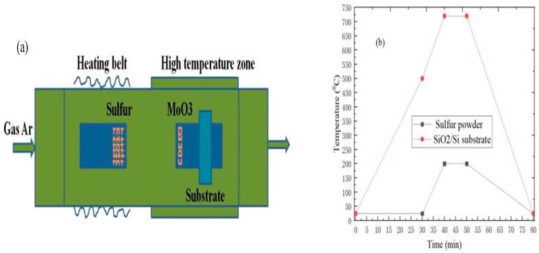
Before the MoS2 growth experiment, SiO2/Si substrates were respectively placed in absolute ethanol, acetone, and deionized water solution for ultrasonic cleaning in 10 min, 10 min, 10 min, and dried with a nitrogen gun. Compared to the reported literature, the difference is that SiO2/Si substrates are cleaned with PCE-6 plasma cleaner under different time and power conditions. Subsequently, different dosages of 1 mg/mL graphene quantum dot solution were applied to SiO2/Si substrates uniformly with oxygen plasma by using VTC-100 vacuum rotary coater. In addition, a quartz boat with 100 mg sulfur powder (Alfa Aesar, Shanghai, China, 99.5%) was transferred to the low temperature zone of the tube furnace constructed by the winding heating belt. Moreover, 2 mg MoO3 powder (Alfa Aesar, Shanghai, China, 99.95%) was weighed into one end of the quartz boat, and SiO2/Si substrate was placed faced down 5 cm apart from the MoO3 powder, and the quartz boat with MoO3 powder and SiO2/Si substrate was placed in the high temperature zone of tube furnace, as shown in Figure 1a. Figure 1b shows the temperature change diagram of MoS2 grown by APCVD, high-purity argon gas with a flow rate of 300 sccm was introduced into the tube furnace for 10 min to exclude air in the tube furnace before the start of the reaction. The high temperature zone of the tube furnace was heated from room temperature to 550 °C in 30 min, meanwhile the heating belt began to heat, and the temperature was controlled at 200 °C. The temperature of the high temperature zone continued to 720 °C in 10 min with heating, and maintained the growth temperature for 10 min before cooling down to room temperature. The temperature distribution in the furnace was as follows: The closer the distance from the intermediate heating zone of the tube furnace was, the higher the temperature was [26,27]. Finally, argon gas with a flow rate of 50 sccm was introduced into the tube furnace throughout the reaction experiment, and the pressure of the tube furnace was maintained at a normal pressure.
Figure 1.
(a) Growth experiment schematic diagram of MoS2; (b) temperature change diagram of MoS2 grown by atmospheric pressure chemical vapor deposition (APCVD).
The new generation high-resolution Raman spectroscopy (LabRAM HR Evolution, HORIBA Jobin Yvon, Paris, France) was used to characterize the surface topography, Raman, and Photoluminescence spectrum of MoS2 systematically. The specific test conditions of the Raman spectroscopy were as follows: 532 nm laser with 1 μm spot diameter, spectral resolution ≤0.65 cm−1, scan time 5 s, and accumulations number 3 s. The layer number of MoS2 could be determined quickly by the difference in the contrast between MoS2 and SiO2/Si substrate under the optical microscope. Raman spectrum was the scattering spectrum that utilized the inelastic scattering effect of the molecules on photons, which can provide an efficient representation of molecular structure. Photoluminescence spectrum is a form of cold luminescence, it would re-emit photons or electromagnetic waves when SiO2/Si substance absorbs photons or electromagnetic waves of a certain frequency. In addition, surface morphology and thickness of MoS2 grown on SiO2/Si substrate were characterized through interatomic interaction forces by using atomic force microscopy with longitudinal high resolution (AFM, Dimension 3100, Veeco Instruments, Shanghai, China). Moreover, X-ray photoelectron spectroscopy-Auger electron spectroscopy (Theta 300 XPS system, Thermo Fisher, Shanghai, China) was also used to measure chemical and electronic states of MoS2.
Optical microscopy (OM) was the most efficient and intuitive method to characterize layered structural materials. MoS2 was grown on silicon substrate with a layer of 285 nm SiO2 by APCVD. The number, size and film formation of MoS2 can be quickly judged by the contrast between MoS2 and SiO2/Si substrate under the optical microscope.
3. Results and Discussion
3.1. Effect of Different Oxygen Plasma Treatment Time and Power on the Growth of MoS2
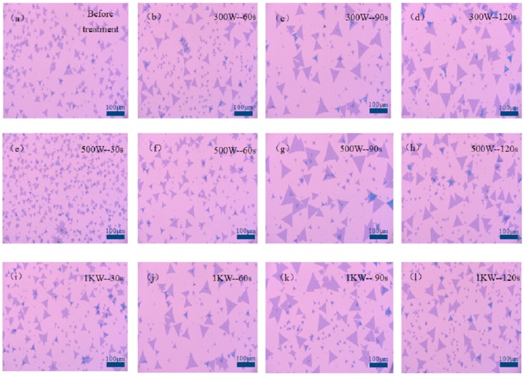
SiO2/Si substrates are cleaned by the PCE-6 oxygen plasma cleaning machine in this experiment. The specific cleaning steps are as follows: First put SiO2/Si substrate into the vacuum chamber and vacuum it to below 1 Pa. Then oxygen gas is introduced to maintain oxygen vacuum in the vacuum chamber to 50 Pa. As the substrate treatment effect is greatly affected by gas pressure, this affects discharge power and processing time during glow discharge. Subsequently, the photo-discharge is performed at the discharge frequency of 13.56 MHz, and SiO2/Si substrates are processed sequentially at 300 W, 500 W, and 1000 W discharge power for 30, 60, 90, and 120 s. The principle of oxygen plasma cleaning is to convert oxygen into its plasma state by the glow discharge. These high-energy ions bombard the surface of the SiO2/Si substrate and easily react with the surface of substrate to increase the surface energy, thereby changing the surface properties of the SiO2/Si substrate and remove the organic impurities of the SiO2/Si substrate surface, which can achieve a hydrophilic effect, and improve the surface activity of the silicon wafer [28]. The characterization of the SiO2/Si substrate before and after oxygen plasma cleaning treatment can be observed by the growth of MoS2. The specific growth of MoS2 under different oxygen plasma treatment time and power are as follows.
It can be found by observing Figure 2 that the growth and morphology of MoS2 would, respectively, become uniform and better, and the size was also improved with an increase of processing time when the oxygen plasma was used in the low-power and medium-power oxygen plasma cleaning of SiO2/Si substrate. This is because the surface roughness is improved significantly after oxygen plasma cleaning, and it can also change the surface characteristics of the SiO2/Si substrate. The growth of MoS2 initially becomes better and more uniform with the increase of processing time when the SiO2/Si substrate is subjected to high-power oxygen plasma cleaning, but the treatment time has almost no effect on the growth of MoS2 after 60 s, which indicates that too long processing time does not always increase the surface activity of the MoS2 material. As the oxygen plasma cleaning power increases, the density and energy of the plasma increase, and the oxygen plasma treatment speed also increases. At this time, the morphology of MoS2 is the triangle with uniform size, and multilayer or bulk materials of MoS2 also appear when the time of cleaning SiO2/Si substrate is constant. As shown in Figure 2, it is found that the optimal oxygen plasma cleaning power and time of SiO2/Si substrate processing are 500 W and 90 s, respectively. At this time, the morphology of MoS2 is the best, and the maximum triangular side length can be up to 100 μm.
Figure 2.
The growth of MoS2 on SiO2/Si substrate under the different oxygen plasma treatment time and power. (a) Before treatment, (b) 300 W, 60 s, (c) 300 W, 90 s, (d) 300 W, 120 s, (e) 500 W, 30 s, (f) 500 W, 60 s, (g) 500 W, 90 s, (h) 500 W, 120 s, (i) 1 KW, 30 s, (j) 1 KW, 60 s, (k) 1 KW, 90 s, (l) 1 KW, 120 s.
3.2. Effect of Graphene Quantum Dot Solution Amount on the Growth of MoS2
Impurities and defects on the SiO2/Si substrate are easily selected when MoS2 sample is deposited by CVD. Therefore, the processing of SiO2/Si substrate would have a greater impact on the nucleation process of MoS2. VTC-100 vacuum rotary coating machine is used to spin the graphene quantum dot solution with a particle size of 2 nm on cleaned SiO2/Si substrate uniformly in the experiment, and research the effect of different dosages of 1mg/ml graphene quantum dot solution on the growth of MoS2 by non-uniform nucleation principle. The size, quality, and continuity of monolayer MoS2 are improved by dropping the graphene quantum dot solution on SiO2/Si substrate.
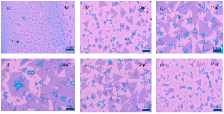
In order to obtain the optimum dosage of graphene quantum dot solution, SiO2/Si substrates with 5 μL, 10 μL, 15 μL, 20 μL, 25 μL, and 30 μL of 1 mg/mL graphene quantum dot solution are carried out on the growth experiments of MoS2. It can be seen from Figure 3 that different dosages of graphene quantum dot solution on SiO2/Si substrates have an effect on growth of MoS2. It can be observed from Figure 3a–d that many small triangles with a size of 20 μm would appear on SiO2/Si substrate under the same growth conditions, the size of the triangular MoS2 increases gradually with graphene quantum dot solution dosage increase, large area continuous film with 300 μm lateral dimension is formed, and the middle of the MoS2 film is obviously thicker. This is because a certain dosage graphene quantum dot solution can provide a suitable nucleation point for MoS2 on SiO2/Si substrate, which would facilitate the growth of a large-area MoS2 film. In Figure 3e,f, MoS2 sample deposited on SiO2/Si substrate is the triangle with a size of 40 μm, and no uniform continuous film is formed. The reason is that the graphene quantum dots solution dosage is too high and the nucleation sites are excessive. In conclusion, the optimal dosage of 1 mg/mL graphene quantum dot solution is 20 μL by analyzing the above results.
Figure 3.
Effect of grapheme quantum dot solution with different dosage on the growth of MoS2. (a) 5μL, (b) 10μL, (c) 15μL, (d) 20μL, (e) 25μL, (f) 30μL.
3.3. The Optimal Growth Conditions of Monolayer MoS2
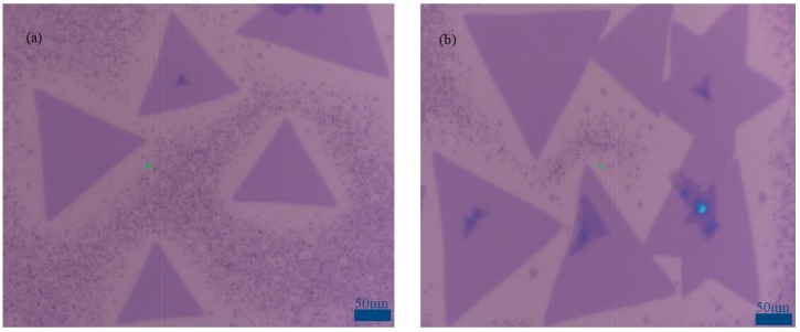
In Figure 4, the size of large-area high-quality monolayer MoS2 grown on SiO2/Si substrate with oxygen plasma (500 w, 90 s) and graphene quantum dot solution (20 μL, 1 mg/mL) can be up to 200 μm, and different monolayer MoS2 spliced together to form large area continuous film with uniform color and good film formation quality. The reason is that a certain dosage graphene quantum dot solution can provide a suitable nucleation point for MoS2, which would contribute to the growth of large-area monolayer MoS2 film. Monolayer MoS2 are characterized by Optical Microscopy, AFM, XPS, Raman, and Photoluminescence Spectroscopy. The following are the test results in detail.
Figure 4.
Growth of different regions MoS2 on SiO2/Si substrate under optimal treatment condition (a) first region; (b) second region Scale bar: 50 μm.
3.4. Characterization of Monolayer MoS2
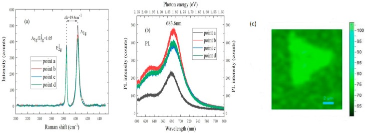
It can be found by observing Figure 5a that there are two characteristic peaks in Raman spectrum of monolayer MoS2. The E12g peak position of in-plane vibration mode is located at 383.3 cm−1, and the A1g peak position of out-of-plane vibration mode is located at 402.7 cm−1, the peak distance between two peaks is 19.4 cm−1, and A1g/E12g ≈ 1.05, which indicates the triangular MoS2 is monolayer [29]. In Figure 5b, monolayer MoS2 film has the strongest luminescence peak at 683.6 nm due to the direct excitation of excitons. It can be known from the conversion relationship between wavelength and electron volts that the corresponding transition energy level at the luminescence peak is about 1.82 eV, and there is also a B peak at 1.98 eV due to the interaction of electrons in the 3d orbital of molybdenum atoms, which can further prove that the sample is a large-area monolayer MoS2 with good film quality [30,31]. In addition, Raman mapping is carried out to observe film-forming quality and uniformity of triangular monolayer MoS2, and the color is very uniform, which also indicates that the sample is monolayer MoS2 with highly uniform quality.
Figure 5.
(a) Raman spectrum, (b) PL spectrum, and (c) mapping of monolayer MoS2 under optimal treatment conditions of SiO2/Si substrate.
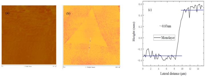
Atomic force microscopy (AFM) is used to characterize the surface topography of layered structural materials. The thickness of MoS2 on SiO2/Si substrate is characterized by AFM, as shown in Figure 6. The film and triangular MoS2 are very uniform in color, and the thickness of MoS2 is about 0.83 nm, which indicates that MoS2 is monolayer.
Figure 6.
(a) Atomic force microscopy (AFM) topography of MoS2 film; (b) AFM topography of triangular MoS2; (c) AFM height profile of triangular MoS2 (blue lines represent the average height of triangular MoS2 under different position).
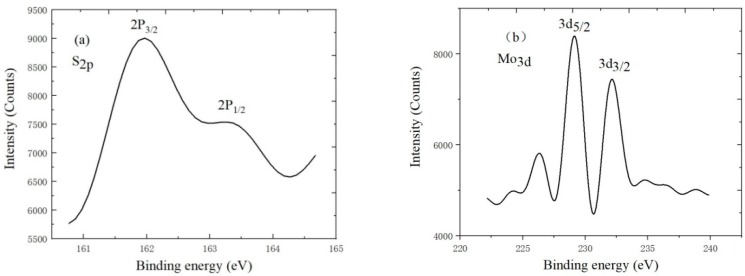
X-ray photoelectron spectroscopy (XPS) is the advanced analytical technique in microscopic analysis of electronic materials and components. It uses photoelectron binding energy as abscissa and relative intensity as ordinate to make photoelectron spectroscopy. The relevant information of MoS2 is obtained by analyzing the energy spectrum. It can be seen from Figure 7 that Mo3d5/2 and 3d3/2 binding energy in Mo4+ is about 228.5 eV and 232.5 eV, respectively. At the same time, 2P3/2 and 2P1/2 binding energy in S2p is about 162.2 eV and 163.3 eV, respectively. The percentages of the S2p element and Mo3d element are 15.79% and 7.58%, respectively, which also indicates MoS2 is monolayer.
Figure 7.
(a) S2p; (b) Mo3d of X-ray photoelectron spectroscopy.
4. Conclusions
In this paper, large-area high-quality uniform triangle monolayer MoS2 is successfully grown on an SiO2/Si substrate with oxygen plasma treatment and graphene quantum dot solution by APCVD. Effects of substrate processing conditions, such as oxygen plasma treatment time, power, and the amount of graphene quantum dot solution on growth quality and the area of monolayer MoS2 are studied in detail. The optimal dosage of 1mg/ml graphene quantum dot solution is 20 μL, and the optimal power and time of SiO2/Si substrate processing are 500 W and 90 s, respectively. Analysis and characterization of monolayer MoS2 are carried out by Optical Microscopy, AFM, XPS Raman, and Photoluminescence Spectroscopy. The results show that the grown sample on the SiO2/Si substrate under optimal cleaning conditions is a large-area high-quality, uniform, triangular monolayer MoS2 with a side length of 200 μm, and it is very effective to treat SiO2/Si substrate by oxygen plasma and graphene quantum dot solution, which can pave the way for the fabrication of optoelectronic devices.
Author Contributions
Conceptualization and writing—original draft preparation, T.H.; methodology, S.W. and S.C.; writing—review and editing, H.L., X.Y., and W.L.; funding acquisition, H.L.
Funding
This research was funded by the National Natural Science Foundation of China (Grant No. U1866212), the Foundation for Fundamental Research of China (Grant No. JSZL2016110B003), the Major Fundamental Research Program of Shaanxi (Grant No. 2017ZDJC-26), innovation Foundation of Radiation Application (Grant No.KFZC2018040206) and supported by 111 project (Grant No. B12026).
Conflicts of Interest
The authors declare no conflict of interest.
References
- 1.Chae W.H., Cain J.D., Hanson E.D., Murthy A.A., Dravid V.P. Substrate-induced strain and charge doping in CVD-grown monolayer MoS2. Appl. Phys. Lett. 2017;111:143106. doi: 10.1063/1.4998284. [DOI] [Google Scholar]
- 2.Li Z., Li Y., Han T., Wang X., Yu Y., Tay B., Liu Z., Fang Z. Tailoring MoS2 exciton—Plasmon interaction by optical spin—Orbit coupling. ACS Nano. 2016;11:1165–1171. doi: 10.1021/acsnano.6b06834. [DOI] [PubMed] [Google Scholar]
- 3.Momeni K., Ji Y., Zhang K., Robinson J.A., Chen L.-Q. Multiscale framework for simulation-guided growth of 2D materials. Npj 2D Mater. Appl. 2018;2:27. doi: 10.1038/s41699-018-0072-4. [DOI] [Google Scholar]
- 4.Xu H., Zhou W., Zheng X., Huang J., Feng X., Ye L., Xu G., Lin F. Control of the nucleation density of molybdenum disulfide in large-scale synthesis using chemical vapor deposition. Materials. 2018;11:870. doi: 10.3390/ma11060870. [DOI] [PMC free article] [PubMed] [Google Scholar]
- 5.Das S., Chen H.-Y., Penumatcha A.V., Appenzeller J. High performance multilayer MoS2 transistors with scandium contacts. Nano Lett. 2013;13:100–105. doi: 10.1021/nl303583v. [DOI] [PubMed] [Google Scholar]
- 6.Li D., Xiao Z., Mu S., Wang F., Liu Y., Song J., Huang X., Jiang L., Xiao J., Liu L. A facile space-confined solid-phase sulfurization strategy for growth of high-quality ultrathin molybdenum disulfide single crystals. Nano Lett. 2018;18:2021–2032. doi: 10.1021/acs.nanolett.7b05473. [DOI] [PubMed] [Google Scholar]
- 7.Vilá R., Momeni K., Wang Q., Bersch B., Lu N., Kim M., Chen L., Robinson J. Bottom-up synthesis of vertically oriented two-dimensional materials. 2D Mater. 2016;3:041003. doi: 10.1088/2053-1583/3/4/041003. [DOI] [Google Scholar]
- 8.Zafar A., Nan H., Zafar Z., Wu Z., Jiang J., You Y., Ni Z. Probing the intrinsic optical quality of CVD grown MoS2. Nano Res. 2017;10:1608–1617. doi: 10.1007/s12274-016-1319-z. [DOI] [Google Scholar]
- 9.Zobel A., Boson A., Wilson P.M., Muratov D.S., Kuznetsov D.V., Sinitskii A. Chemical vapour deposition and characterization of uniform bilayer and trilayer MoS2 crystals. J. Mater. Chem. C. 2016;4:11081–11087. doi: 10.1039/C6TC03587F. [DOI] [Google Scholar]
- 10.Bertolazzi S., Krasnozhon D., Kis A. Nonvolatile memory cells based on MoS2/graphene heterostructures. ACS Nano. 2013;7:3246. doi: 10.1021/nn3059136. [DOI] [PubMed] [Google Scholar]
- 11.Zhang F., Momeni K., AlSaud M.A., Azizi A., Hainey M.F., Jr., Redwing J.M., Chen L.-Q., Alem N. Controlled synthesis of 2D transition metal dichalcogenides: From vertical to planar MoS2. 2D Mater. 2017;4:025029. doi: 10.1088/2053-1583/aa5b01. [DOI] [Google Scholar]
- 12.Ning F., Wang D., Feng Y.-X., Tang L.-M., Zhang Y., Chen K.-Q. Strong interfacial interaction and enhanced optical absorption in graphene/InAs and MoS2/InAs heterostructures. J. Mater. Chem. C. 2017;5:9429–9438. doi: 10.1039/C7TC03350H. [DOI] [Google Scholar]
- 13.Sundaram R., Engel M., Lombardo A., Krupke R., Ferrari A., Avouris P., Steiner M. Electroluminescence in single layer MoS2. Nano Lett. 2013;13:1416–1421. doi: 10.1021/nl400516a. [DOI] [PubMed] [Google Scholar]
- 14.Jia G.Y., Liu Y., Gong J.Y., Lei D.Y., Wang D.L., Huang Z.X. Excitonic quantum confinement modified optical conductivity of monolayer and few-layered MoS2. J. Mater. Chem. C. 2016;4:8822–8828. doi: 10.1039/C6TC02502A. [DOI] [Google Scholar]
- 15.Novoselov K., Jiang D., Schedin F., Booth T., Khotkevich V., Morozov S., Geim A. Two-dimensional atomic crystals. Proc. Natl. Acad. Sci. USA. 2005;102:10451–10453. doi: 10.1073/pnas.0502848102. [DOI] [PMC free article] [PubMed] [Google Scholar]
- 16.Jiang L., Lin B., Li X., Song X., Xia H., Li L., Zeng H. Monolayer MoS2–graphene hybrid aerogels with controllable porosity for lithium-ion batteries with high reversible capacity. ACS Appl. Mater. Interfaces. 2016;8:2680–2687. doi: 10.1021/acsami.5b10692. [DOI] [PubMed] [Google Scholar]
- 17.Plechinger G., Mann J., Preciado E., Barroso D., Nguyen A., Eroms J., Schueller C., Bartels L., Korn T. A direct comparison of CVD-grown and exfoliated MoS2 using optical spectroscopy. Semicond. Sci. Technol. 2014;29:064008. doi: 10.1088/0268-1242/29/6/064008. [DOI] [Google Scholar]
- 18.Zhang Y., Xu L., Walker W.R., Tittle C.M., Backhouse C.J., Pope M.A. Langmuir films and uniform, large area, transparent coatings of chemically exfoliated MoS2 single layers. J. Mater. Chem. C. 2017;5:11275–11287. doi: 10.1039/C7TC02637D. [DOI] [Google Scholar]
- 19.Wu J., Dai J., Shao Y., Cao M., Wu X. Carbon dot-assisted hydrothermal synthesis of flower-like MoS2 nanospheres constructed by few-layered multiphase MoS2 nanosheets for supercapacitors. RSC Adv. 2016;6:77999–78007. doi: 10.1039/C6RA15074H. [DOI] [Google Scholar]
- 20.Fadil D., Hossain R.F., Saenz G.A., Kaul A.B. On the chemically-assisted excitonic enhancement in environmentally-friendly solution dispersions of two-dimensional MoS2 and WS2. J. Mater. Chem. C. 2017;5:5323–5333. doi: 10.1039/C7TC01001J. [DOI] [Google Scholar]
- 21.Li Z., Ye R., Feng R., Kang Y., Zhu X., Tour J.M., Fang Z. Graphene quantum dots doping of MoS2 monolayers. Adv. Mater. 2015;27:5235–5240. doi: 10.1002/adma.201501888. [DOI] [PubMed] [Google Scholar]
- 22.Rukelj Z., Štrkalj A., Despoja V. Optical absorption and transmission in a molybdenum disulfide monolayer. Phys. Rev. B. 2016;94:115428. doi: 10.1103/PhysRevB.94.115428. [DOI] [Google Scholar]
- 23.Choudhury P., Ravavarapu L., Dekle R., Chowdhury S. Modulating Electronic and Optical Properties of Monolayer MoS2 Using Nonbonded Phthalocyanine Molecules. J. Phys. Chem. C. 2017;121:2959–2967. doi: 10.1021/acs.jpcc.6b11239. [DOI] [Google Scholar]
- 24.Qiu D., Lee D.U., Pak S.W., Kim E.K. Structural and optical properties of MoS2 layers grown by successive two-step chemical vapor deposition method. Thin Solid Films. 2015;587:47–51. doi: 10.1016/j.tsf.2015.01.036. [DOI] [Google Scholar]
- 25.Late D.J., Huang Y.-K., Liu B., Acharya J., Shirodkar S.N., Luo J.J., Yan A., Charles D., Waghmare U.V., Dravid V.P., Rao C.N.R. Sensing behavior of atomically thin-layered MoS2 transistors. ACS Nano. 2013;7:4879. doi: 10.1021/nn400026u. [DOI] [PubMed] [Google Scholar]
- 26.He J., Fernández C., Primo A., Garcia H. One-Step Preparation of Large Area Films of Oriented MoS2 Nanoparticles on Multilayer Graphene and Its Electrocatalytic Activity for Hydrogen Evolution. Materials. 2018;11:168. doi: 10.3390/ma11010168. [DOI] [PMC free article] [PubMed] [Google Scholar]
- 27.Shastry T.A., Balla I., Bergeron H., Amsterdam S.H., Marks T.J., Hersam M.C. Mutual photoluminescence quenching and photovoltaic effect in large-area single-layer MoS2–polymer heterojunctions. ACS Nano. 2016;10:10573–10579. doi: 10.1021/acsnano.6b06592. [DOI] [PubMed] [Google Scholar]
- 28.Serna M.I., Yoo S.H., Moreno S., Xi Y., Oviedo J.P., Choi H., Alshareef H.N., Kim M.J., Minary-Jolandan M., Quevedo-Lopez M.A. Large-area deposition of MoS2 by pulsed laser deposition with in situ thickness control. ACS Nano. 2016;10:6054–6061. doi: 10.1021/acsnano.6b01636. [DOI] [PubMed] [Google Scholar]
- 29.Yu F., Liu Q., Gan X., Hu M., Zhang T., Li C., Kang F., Terrones M., Lv R. Ultrasensitive Pressure Detection of Few—Layer MoS2. Adv. Mater. 2017;29:1603266. doi: 10.1002/adma.201603266. [DOI] [PubMed] [Google Scholar]
- 30.Lopez-Sanchez O., Alarcon Llado E., Koman V., Fontcuberta i Morral A., Radenovic A., Kis A. Light generation and harvesting in a van der Waals heterostructure. ACS Nano. 2014;8:3042–3048. doi: 10.1021/nn500480u. [DOI] [PMC free article] [PubMed] [Google Scholar]
- 31.Yin Z., Li H., Li H., Jiang L., Shi Y., Sun Y., Lu G., Zhang Q., Chen X., Zhang H. Single-layer MoS2 phototransistors. ACS Nano. 2011;6:74–80. doi: 10.1021/nn2024557. [DOI] [PubMed] [Google Scholar]


