Abstract
A Si wafer coated with a low temperature oxide (LTO) was used as substrate (Si/SiO2) during the deposition of a thick nano-crystalline graphite (NCG) film by means of plasma-enhanced chemical vapour deposition (PECVD) procedure. The process parameters, the atomic force (AFM) and scanning electron (SEM) micrographs, Raman spectrum and X-ray diffraction (XRD) pattern are herein illustrated. The as deposited NCG film was electrochemically pretreated (3 mA applied current, during 240 s, in 10 mM phosphate buffer saline (PBS) solution containing 0.1 M KCl, pH 7) and thereafter used as electrode for sensing the caffeic acid content in lyophilised berries and dried chokeberries in “Nano-crystalline graphite film on SiO2: Electrochemistry and electro-analytical application” [1].
Keywords: Plasma-enhanced chemical vapour deposition (PECVD), Nano-crystalline graphite (NCG), Electrochemistry, Caffeic acid
Specifications table
| Subject area | Electrochemistry, Materials science, Nanotechnology |
| More specific subject area | Electrode material development |
| Type of data | Image (atomic force microscopy – AFM, scanning electron microscopy – SEM), graph (Raman spectroscopy, X-ray diffraction – XRD), table (process parameters for using plasma-enhanced chemical vapour deposition – PECVD). |
| How data was acquired | Atomic force microscope (Ntegra Aura Scanning Probe Microscope, NT_MDT Spectrum Instruments) operated in intermittent-contact mode; scanning electron microscope (Nova NanoSEM 630, FEI Company, USA) working at 20 kV accelerating voltage, under high vacuum (HV) conditions and using Through the Lens Detector (TLD); confocal microscope (WITec alpha300 S, WITec, GmbH, Germany) with a 20X lens and 532 nm excitation wavelength was used to acquire the Raman spectrum; 9kW rotating anode X-ray diffraction system (Rigaku SmartLab, Japan) that employs Cu Kα1 radiation (λ = 1.54056 Å); PECVD growth (NANOFAB 1000, Oxford Instruments, UK). |
| Data format | Raw, analyzed |
| Experimental factors | Electrochemical activation of the nano-crystalline graphite film at 3 mA applied current, during 240 s, in 10 mM phosphate buffer saline (PBS) solution containing 0.1 M KCl, pH 7. |
| Experimental features | A 4″, Si-n, <100>, 1–3 Ω cm wafer bearing 110 nm SiO2 was heated up to 900 °C (15 °C min−1) in Ar/H2 (5%) atmosphere, annealed during 10 minutes, allowing an additional surface hydrogenation step for 5 more minutes in Ar/H2 (10%) atmosphere, after the ultimate process temperature was reached. The nano-crystalline graphite (NCG) film was grown starting from CH4 and H2 (60 sccm/75 sccm), using 100 W power plasma, at 900 °C and 1.5 Torr, up to a thickness of ∼350 nm. The working parameters of the PECVD process are detailed in Table 1. The NCG film grew on Si/SiO2 substrate was used as working electrode during several electrochemical investigations, alongside with Ag/AgCl reference electrode and Pt wire serving as counter electrode. |
| Data source location | National Institute for Research and Development in Microtechnology – IMT Bucharest, 126A Erou Iancu Nicolae Street, 077190, Voluntari, Ilfov county, Romania |
| Data accessibility | The data presented in this article are accessible within this article. |
| Related research article | C. Albu, S.A.V. Eremia, M.L. Veca, A. Avram, R.C. Popa, C. Pachiu, C. Romanitan, M. Kusko, R. Gavrila, A. Radoi, Nano-crystalline graphite film on SiO2: Electrochemistry and electro-analytical application, Electrochim. Acta, 303, 2019, 284–292 [1]. |
Value of the data
|
1. Data
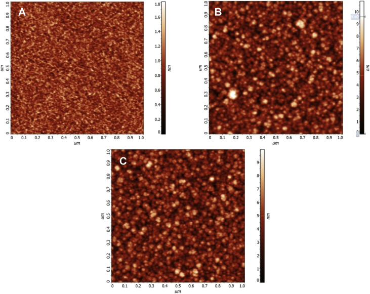
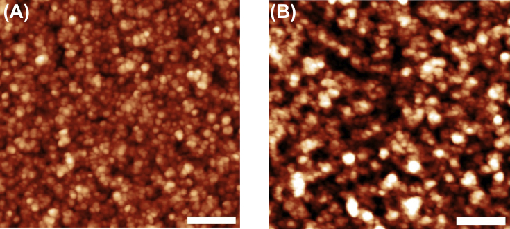
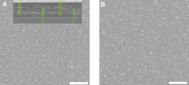
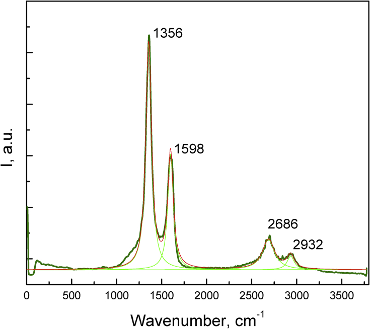
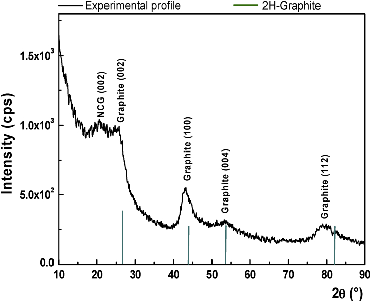
The data are Supplementary materials paired with “Nano-crystalline graphite film on SiO2: electrochemistry and electro-analytical application” [1]. AFM micrographs in Fig. 1 are illustrating the Si substrate- RMS 0.15 nm (A), the Si/LTO substrate– RMS 1.4 nm (B) and the Si/LTO –annealed substrate– RMS – 1.3 nm (C). Fig. 2 shows typical morphologies, acquired using atomic force microscopy (AFM), of the NCG film before (A) and after the electrochemical pretreatment (B). Fig. 3 reports SEM micrographs before (A) and after the electrochemical activation (B). The thickness for the NCG film (∼350 nm) and the LTO deposited SiO2 (110 nm) is illustrated in Fig. 3A – inset. Fig. 4 exemplify the obtained Raman spectra acquired at 532 nm, using the confocal microscope WITec alpha300 S. X-ray diffraction pattern for nano-crystalline graphite (NCG) film is reported in Fig. 5. Table 1 provides the process parameters for LTO annealing and NCG growth achieved using the PECVD approach.
Fig. 1.
AFM illustrating (A) Si substrate- RMS 0.15 nm; (B) Si/LTO substrate– RMS 1.4 nm; and (C) Si/LTO –annealed substrate– RMS – 1.3 nm.
Fig. 2.
Atomic force microscopy (AFM) imaging before (A) and after (B) the electrochemical activation (scale bar: 200 nm).
Fig. 3.
SEM micrographs before (A) and after the electrochemical activation (B) (scale bar: 300 nm).
Fig. 4.
Raman spectra acquired at 532 nm; Lorentzian multiple peak fitting was used.
Fig. 5.
X-ray diffraction (XRD) pattern for nano-crystalline graphite (NCG) film.
Table 1.
Process parameters for LTO annealing and NCG growth.
| T, (°C) | t, (min) | Heat ramp (°C/min) | PRF., (W) | P, (mTorr) | Ar flow (sccm) | H2 flow (sccm) | CH4 flow (sccm) | |
|---|---|---|---|---|---|---|---|---|
| Heat-up | 200↗900 | – | 15 | – | 3000 | 1500 | 75 | – |
| Si/SiO2 (LTO) annealing | 900 | 10 | – | – | 3000 | 1500 | 75 | |
| Hydrogen annealing | 900 | 5 | – | – | 1500 | 1500 | 200 | – |
| Deposition | 900 | 120 | – | 100 | 1500 | – | 75 | 60 |
| Cool-down | 900↘200 | – | 9 | – | 1500 | 1500 | – | – |
2. Experimental design, materials and methods
Atomic force microscopy scans on bare Si wafer, Si/LTO –annealed substrate, as PECVD deposited nano-crystalline graphite film (NCG) and electrochemically etched NCG film, have been performed in intermittent-contact mode, using AFM probes provided with high aspect ratio tips (7:1, Olympus OMCL-AC240BSA) having 5–10 nm nominal radius. The micrographs were obtained using the Nova NanoSEM 630 (FEI Company, USA) scanning electron microscope (SEM). The Raman spectrum was acquired at 532 nm excitation wavelength using a with a WITec alpha300 S (WITec, GmbH, Germany) confocal microscope with a 20X lens; calibration was performed on the 520 nm Raman shift of Si. X-ray diffraction pattern of the NCG layer was obtained using a 9kW rotating anode (Rigaku SmartLab, Japan) that employs Cu Kα1 radiation (λ = 1.54056 Å). The electrochemical treatment (3 mA applied current, during 240 s) of the NCG film was performed using the Autolab electrochemical system model PGSTAT 302 N (Eco Chemie, The Netherlands) and a flat cell from Bio-Logic SAS (http://www.bio-logic.net/) in a three-electrode configuration, i.e. the working electrode being the NCG layer, the reference electrode was Ag/AgCl and as counter electrode a Pt wire was used. The electrolyte consisted of 10 mM phosphate buffer saline (PBS) solution, pH 7, supplemented with 0.1 M KCl. A Si/SiO2 substrate (4″, Si-n, <100>, 1–3 Ω cm wafer with 110 nm low temperature oxide) was heated up to 900 °C (15 °C min−1) in Ar/H2 (5%) atmosphere, annealed during 10 minutes, additionally treated 5 more minutes in Ar/H2 (10%) atmosphere, after reaching the ultimate process temperature. The nano-crystalline graphite (NCG) film was grown starting from CH4 and H2 (60 sccm/75 sccm), using 100 W power plasma, at 900 °C and 1.5 Torr, up to a thickness of ∼350 nm.
Acknowledgments
C. Albu and S. A. V. Eremia acknowledge financial support offered by the Core Program PN 18180103/2018 – BIODIVERS 2 funded by MCI. A. Radoi, M. L. Veca, R. C. Popa and C. Pachiu acknowledge financial support offered by the Core Program PN 18 08/4 N/16.03.2018 – MICRO-NANO-SIS and PN 1916/2019 – MICRO-NANO-SIS PLUS/08.02.2019 funded by MCI. A. Radoi also acknowledges financial support offered by PN—III—P1-1.2-PCCDI2017-0619 – Project no. 3.
Footnotes
Transparency document associated with this article can be found in the online version at https://doi.org/10.1016/j.dib.2019.103923.
Contributor Information
Sandra A.V. Eremia, Email: sandraeremia@gmail.com.
Antonio Radoi, Email: radoiantonio@yahoo.com.
Transparency document
The following is the transparency document related to this article:
Reference
- 1.Albu Camelia, Eremia Sandra A.V., Veca Monica Lucia, Avram Andrei, Popa Radu Cristian, Pachiu Cristina, Romanitan Cosmin, Kusko Mihaela, Gavrila Raluca, Radoi Antonio. Nano-crystalline graphite film on SiO2: electrochemistry and electro-analytical application. Electrochim. Acta. 2019;303:284–292. [Google Scholar]
Associated Data
This section collects any data citations, data availability statements, or supplementary materials included in this article.


