Abstract
Two brain signal acquisition (BSA) front-ends incorporating two CMOS ultra-low power low noise amplifier arrays and serializers operating in MOSFET weak inversion region are presented. To boost the amplifier’s gain for a given current budget, cross-coupled-pair active load topology is used in the first stages of these two amplifiers. These two BSA front-ends are fabricated in 130 nm and 180nm CMOS processes, occupying 5.45 mm2 and 0.352 mm2 of die areas, respectively (excluding pad rings). The CMOS 130 nm amplifier array is comprised of 64 elements, where each amplifier element consumes 0.216 μW from 0.4 V supply, has input-referred noise voltage (IRNoise) of 2.19 μVRMS corresponding to a power efficiency factor (PEF) of 11.7 and occupies 0.044 mm2 of die area. The CMOS 180 nm amplifier array employs 4 elements, where each element consumes 0.69 μW from 0.6 V supply with IRNoise of 2.3 μVRMS (corresponding to a PEF of 31.3) and 0.051 mm2 of die area. Non-invasive electroencephalographic (EEG) and invasive electrocorticographic (ECoG) signals were recorded real-time directly on able-bodied human subjects, showing feasibility of using these analog front-ends (AFEs) for future fully implantable brain signal acquisition and brain computer interface systems.
Keywords: CMOS, Electrocorticography (ECoG), Electroencephalogram (EEG), ultra-low power (ULP), noise efficiency factor (NEF), power efficiency factor (PEF), operational transconductance amplifier (OTA), instrumentation amplifier (InAmp), analog front-end (AFE), weak inversion (WI) region
I. Introduction
IT is estimated that every year there are ~500,000 new cases of spinal cord injury (SCI) worldwide [1]. This condition substantially decreases independence and quality of life of those affected, and the resulting disability and comorbidities pose a significant economic burden on the individual as well as on society. Since there are no satisfactory means to restore motor function after SCI, novel approaches to address this problem are needed. Bypassing the damaged spinal cord by means of a brain-computer interface (BCI), which enables direct brain control of prostheses, constitutes one such approach. Non-invasive electroencephalogram (EEG)-based BCIs have the capacity to restore basic ambulation after SCI [2], [3], although their applicability is limited by the low information content (i.e., limited bandwidth and low spatial resolution) of EEG signals. Invasive BCIs, on the other hand, have enabled control of multi-degree-of-freedom robotic prostheses [4]. However, they utilize bulky and power-hungry generalpurpose recording hardware, and rely on skull-protruding electronic components. Furthermore, these systems typically employ intracortically implanted microelectrode arrays, which can trigger foreign body responses such as inflammation and scarring, ultimately leading to failure of the system within months to few years [5]. These factors represent a serious obstacle to a widespread adoption of invasive BCI technology.
These problems may be addressed by developing a fully implantable BCI system that uses highly stable electrocorticogram (ECoG) signals [6]. Such a BCI system is envisioned to consist of ECoG electrodes, amplifiers, a processor, and a wireless module to control and communicate with output devices (e.g., prostheses), all implemented in a miniaturized form factor and operating in a low-power regime in order to facilitate permanent implantation. Since ECoG electrodes are placed above the arachnoid layer without breaching the neuronal tissue, ECoG signals have long-term stability [6], [7], while providing the spatiotemporal resolution necessary for high-performance BCI applications [8], [9]. In particular, studies have shown that the ECoG high-γ frequency band (70–120 Hz) exhibits spatially localized amplitude modulation that is correlated with individual’s physical movements [10], and this feature has been used to decode arm [11] and finger movements [12]. Chronic in vivo recording of ECoG signals has been used for neurological treatment. The Medtronic Activa PC+S system [13], [14], was used in patients having Parkinson disease with ECoG electrode strips implanted over the motor cortex and depth electrodes in the subthalamic nucleus [15]. Chronic recordings from these areas were used to study the association between gamma band oscillations and dyskinesia. The Activa PC+S system was also used for recording signals from ECoG electrode strips over the motor cortex of a patient with amyotrophic lateral sclerosis (ALS) to facilitate BCI-control of a virtual keyboard [16]. Finally, as shown in prior art, a fully implantable system eliminates the need for bulky skull-protruding components, often employed in the state-of-the-art invasive BCIs, as well as bulky recording hardware and external computers.
There has been extensive research on low-power amplifier and amplifier array designs for neural signal sensing applications, which vary substantially in frequency and dynamic range. For example, in [17], the authors present a folded-cascode operational transconductance amplifier (OTA) using current-splitting and current-scaling techniques with a cascaded 6th-order band-pass filter for detecting epileptic fast ripples between 250 and 500 Hz. The stack of 4 transistors and large degeneration resistors in this design increase the required supply voltage to accommodate sufficient output voltage headroom. In [18], a closed-loop neural recording amplifier has been developed that utilizes a T-network in its feedback path in order to achieve high input impedance and common-mode rejection ratio (CMRR) within a small chip area. The authors argued that the T-network in the feedback path is useful when the routing area overhead, crosstalk and input-referred noise (IRNoise) do not dominate the performance [18].
Most of the previously developed neural sensing amplifiers focus on EEG or single-unit recordings. Consequently, their designs are not optimal for use in other recording modalities, such as ECoG. Moreover, a few studies that exist with analog front-end (AFE) designs for ECoG recording lack in vivo experimental validation in humans. For example, [19] presents a 32-channel integrated circuit (IC) for ECoG recording, followed by in vivo measurements in a rat. The power consumption of this system is too high, making it unsuitable for human ECoG signal acquisition, especially in a fully implantable form. In [20], an ECoG/EEG IC has been introduced which records signals in 4 different sub-bands as opposed to simultaneously capturing the complete ECoG spectrum. This IC has been validated by comparing the measurements of a pre-recorded human ECoG signal with those generated by a model of the signal acquisition chain. This approach, however, does not accurately capture the IC’s interface with the body (e.g. 60 Hz noise), which may significantly affect the performance. When tested in an awake monkey, the signals simultaneously measured by this IC and those acquired using a commercial system showed only modest correlations in α (8–12 Hz) and high-γ (70–120 Hz) bands. This can be explained by the dominating effects of flicker and thermal noise at these frequencies. On the other hand, the signals in the β (13–35 Hz) and low-γ (35–70 Hz) bands were only qualitatively compared with no correlation coefficients reported. Recent work [21] reports on an AFE consuming 1.08 μW of power per channel, which is achieved by narrowing the AFE bandwidth and filtering out the noise. A potential problem with this approach may lie in the high sensitivity of the designed GmC filters to process variation. The proposed AFE has been tested in its ability to reproduce pre-recorded ECoG data and acquire ECoG signals in vivo from an anesthetized monkey. However, human testing and direct comparison of recorded signals to those acquired with a commercial-grade system have not been performed. Finally, the work in [22] presents a 64-channel wireless micro ECoG recording system with the front-end achieving a power-efficiency factor (PEF) that is 3× smaller than the state-of-the-art. In vivo measurements from an anesthetized rodent show the power increase with respect to the pre-sedation state in δ (1–4 Hz) and θ (4–7 Hz) bands, but very little change in BCI-relevant frequency bands. Furthermore, none of the above systems were tested in a hospital environment, which is typically characterized by extremely hostile ambient noise and interference conditions. In summary, while the development of these architectures has been inspired by human BCI applications, their in vivo testing in humans and comparison to conventionally acquired ECoG signals are conspicuously missing.
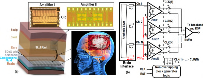
This paper presents the design, experimental validation, and comparative study of two CMOS ultra-low power (ULP) amplifier array and serialization circuitries that constitute core building blocks of two brain signal acquisition (BSA) front-ends. These BSA front-ends can act as the basis for a future, fully implantable ECoG-based BCI system (Fig. 1(a)). The AFE IC will be housed within an enclosure, called the skull unit, to be surgically implanted into the skull [23]. Other building blocks required to develop a complete ECoG-based BCI, e.g., transceiver, power management unit and digital signal processor are intended to be placed in another unit away from the patient’s brain. This approach imposes less health hazards for the patient as well as more practical system specifications for a portable, user-friendly solution. All circuits in this work are designed to operate in the weak inversion (WI) region to maximize power efficiency and minimize heat dissipation, while maintaining high gain and low noise operation. In vivo human measurements and objective validation against a commercial bioamplifier are done in (1) a human subject using non-invasive EEG cap, and (2) a human subject with subdurally implanted high-density ECoG grid.
Fig. 1.
Proposed AFE: (a) A cross-sectional view of the envisioned fully implantable BSA circuit, enclosed within a skull unit module. The BSA circuit is connected to a subdurally implanted high-density (HD)-ECoG electrode grid that senses brain signals. (b) Block diagram of the structure showing the brain interface electrodes with their corresponding impedances and BSA comprised of an array of fully differential amplifiers, serializer and buffer.
The paper is organized as follows. Section II presents the proposed AFE for recording ECoG signals and identifies the criteria and required specifications of the building blocks for designing the system. Sections III and IV discuss the design and implementation of the two BSA front-ends, BSA I and BSA II, respectively. Section V illustrates the electrical and neural measurement results of both front-ends. Finally, Section VI presents concluding remarks and potential extensions of this work.
II. Proposed System Architecture
Responsible for sensing and amplification of microvolt-level brain signals, the amplifier array IC is a critical building block of a BSA front-end. To be employed as a fully implantable device, the signal acquisition front-end should be small in size and consume micro-watt level of power. The system-level diagram of the proposed AFE is shown in Fig. 1(b) [24]. The AFE IC includes fully differential amplifiers, a serializer, and an output buffer all biased in the WI region. The outputs of the array are multiplexed in time to better facilitate inputoutput cable management by reducing the number of wires. The non-overlapping clock generator within the serializer generates N-phase clock signals, each with 1/N duty cycle. Non-overlapping clock signals ensure that only one amplifier is connected to the output buffer at a time during the channel switchover. This work presents two ULP BSA front-ends, BSA I and BSA II. BSA I provides symmetrical and complementary signal amplification paths to achieve energy-efficient low noise signal conditioning. BSA II is designed to achieve a high CMRR (i.e., better than 70 dB), thereby reducing the detrimental effect of power-line 60 Hz interference on the recorded signal.
Minimizing both noise and power dissipation imposes stringent design trade-off in an AFE for an implantable system, mandating meticulous considerations at every level of the design process. For example, at the device level, this notion implies that transistors should be designed to operate in a region which yields minimum power consumption for a given IRNoise imposed by minimum detectable ECoG signal power.
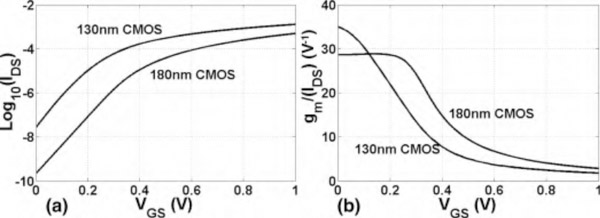
It is well-known that the MOS transistors in the WI region achieve maximum gm/IDS-ratio, resulting in the highest power efficiency at the cost of lower operation maximum bandwidth [25], [26]. Fig. 2 demonstrates gm/IDS and log10(IDS) variations with respect to VGS for the two technologies given the same transistor sizes and bias conditions. Referring to Fig. 2(a), a higher subthreshold leakage current and a higher slope are observed in the weak-inversion region for the 130nm process compared to the 180nm process. A higher slope corresponds to a larger gm for the same bias current. This feature translates to a better power efficiency (Fig. 2(b)) and noise performance for transistors designed in this specific 130nm process. It is noteworthy that the gm/IDS-plot for the 130 nm CMOS process does not show the expected flat region in the deep subthreshold region. This is because BSIM4 device model was adopted for this process by the foundry. On the other hand, the 180 nm process employed PSP device model, which can predict the device behavior in deep subthreshold region more accurately.
Fig. 2.
(a) Drain-source current (Ids) vs. gate-source voltage (Vgs) for the two technologies. (b) gm/IDS vs. Vgs for the two technologies. W/L = 20μm/2μm with 10 fingers, Vds = 1V for both transistors and body temperature of 37 is considered for simulation.
ECoG signals typically have an amplitude of around 50–100 μV [27], with β and high-γ bands typically providing the most informative features for BCI applications [10]. The IRNoise of the AFE should be kept lower than the noise floor of the ECoG electrodes. Our recorded measurements using a commercial BCI signal acquisition equipment showed that the RMS noise floor, integrated over a frequency range of 8–200 Hz, is typically less than 10 μVRMS, which is in compliance with the data reported in literature, e.g. [28]. Low noise operation is of particular interest for high-γ band, because the ECoG signal power becomes weaker with frequency [29].
The CMRR and power-supply rejection ratios (PSRR) should be large to attenuate the effect of environmental noise sources (e.g., 60 Hz power-line noise). Assuming an IRNoise level of 2μVRMS in the presence of common-mode interference with 10 mVRMS, a nominal 34 dB attenuation (i.e., 74 dB CMRR) is needed so that the output noise and interference voltage magnitudes are equal. In addition, the amplifier should show a high input impedance to lower the effect of common-mode interference. This attribute is especially important for multi-channel recordings since the impedance mismatch between electrodes (Ze,1, ..., Ze,N) as well as the mismatch between the impedance seen from the common reference input (parallel combination of Zin,1, ..., Zin,N in Fig. 1) and Zin,k (1 ≤ k ≤ N) reduces the overall CMRR. Subdural electrodes’ impedance have been reported (as well as measured) to be about 1 kΩ [6], thus the input impedance at the frequency of interest should be ≫ 1 MΩ [30]. Moreover, large DC offset associated with neural recording electrodes should be eliminated so as to minimize distortion or avoid saturation of the amplifier. Furthermore, electrical shielding and DC isolation are needed between the IC and implanted electrodes. Finally, the crosstalk in a multi-channel system should be mitigated to avoid contamination of the overall information recorded from different channels.
III. BSA I: An Array of 64 Amplifier I Circuits and A Serializer
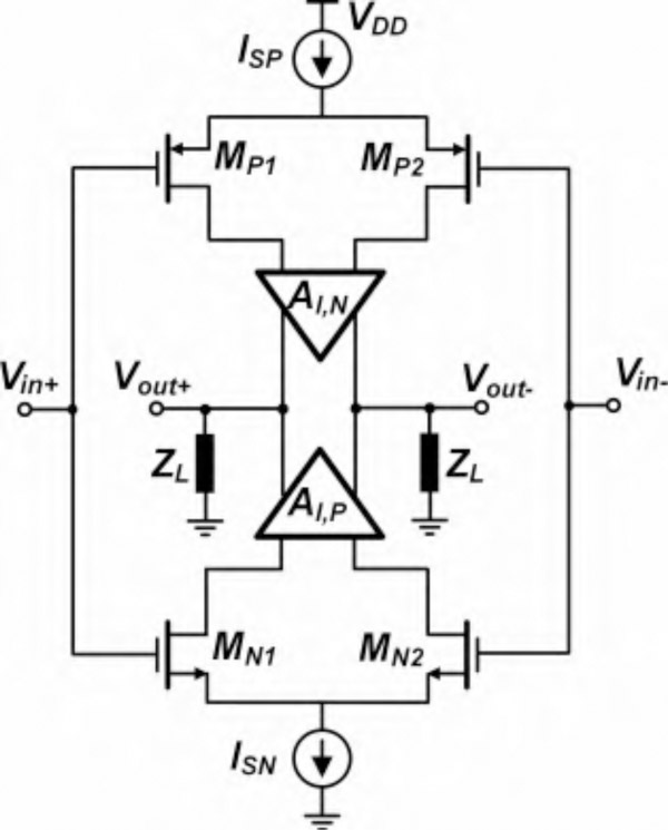
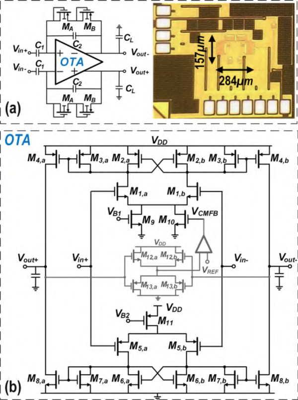
BSA I incorporates 64 units of Amplifier I and a serializer, as shown in Fig. 1(b). Fig. 3 shows the general block diagram of the OTA used in the Amplifier I, composed of complementary NMOS-PMOS input stage. Intuitively, the signal is amplified by the transconductance gain of the input transistor pairs and subsequently applied to the current gain stage in each of the top and bottom branches (AI,N and AI,P). Upon flowing through the load impedance ZL, the summing current will generate the output voltage. Fig. 4(a) shows the top-level topology of Amplifier I employing an OTA with an RC feedback network. The AC-coupled input provides DC rejection between the recording electrodes and the OTA input, thus providing a layer of electrical safety and isolation between the patient’s brain and the amplifier. Fig. 4(b) depicts the transistor-level schematic of the OTA utilized in Amplifier I, including common-mode feedback (CMFB) circuitry (in gray) [23]. The OTA device sizes and aspect-ratios together with operating points of the individual devices are presented in Table I. NMOS and PMOS transistors’ body connections are tied to the ground and supply rails, respectively. The minimum headroom for a single transistor biased in the WI region is ~4UT (where UT ≈ 26 mV at room temperature) [31]. As a result, the OTA is biased at 0.4 V supply to mitigate large process variations resulting from WI operation, while achieving low power and low noise. The first stage employs a complementary NMOS-PMOS differential configuration with a complementary active load comprising parallel combination of diode-connected transistors and a cross-coupled pair [23], [32]. Cross-coupled pair and diode-connected transistors are identically sized as shown in Table I, thereby having the same transconductance. The effective output resistance of the input stage is thus increased from (in the absence of cross-coupled pair load) to ro1∥ro2∥ro3, where ro1, ro2 and ro3 are the drain resistance of M1, M2 and M3, respectively. The active-load devices are sized in a way that no instability or latch-up happens due to the process variation. The size of output transistors M4 and M8 are chosen to exhibit large drain resistance and low current consumption at the output stage.
Fig. 3.
Complementary input structure of the OTA used in Amplifier I
Fig. 4.
(a) Amplifier I comprising a closed-loop amplifier with capacitive feedback and its die microphotograph, and (b) the schematic of the complementary NMOS-PMOS OTA [23]
TABLE I.
Amplifier I device sizes and operating points
| Devices | W/L (μm/μm) | ID (nA) | gm/ID (V−1) |
|---|---|---|---|
| M1a-M1b | 53.5/1.35 | 130 | 34 |
| M2a-M2b | 50/10 | 65 | 25 |
| M3a-M3b | 50/10 | 65 | 25 |
| M4a-M4b | 3.7/32 | 1.5 | 25 |
| M5a-M5b | 140/1.2 | 138 | 29 |
| M6a-M6b | 15/30 | 69 | 28 |
| M7a-M7b | 15/30 | 69 | 28 |
| M8a-M8b | 0.4/40 | 1.5 | 26 |
| M9 | 80/0.36 | 89 | 34 |
| M10 | 80/0.36 | 170 | 35 |
| M11 | 120/0.13 | 277 | 25 |
The capacitance ratio C1/C2 (C1 = 20 pF and C2 = 200 fF) defines the closed-loop gain with high accuracy so long as the open-loop gain is sufficiently high. High output impedance of the OTA imposes a high impedance load for the feedback and next stage circuits. Pseudo-resistors realized by transistors Ma and Mb (as in [33]) provide large equivalent resistance R of few GΩ, self-bias the input stage of the OTA without consuming any additional power for closing the loop, and set the lower 3-dB cutoff frequency (fL = (2πRC2)−1). Compared to pseudo-resistor used in [34], this implementation provides a wider linear range of operation. Assuming all transistors are identically matched (to simplify the analysis), the IRNoise power spectral density (PSD) of the open-loop OTA is calculated to be:
| (1) |
where k is the Boltzmann constant, γ, Kp,1/f and Kn,1/f are technology-dependent parameters, f is frequency, Cox is the gate oxide capacitor, and T is the temperature. γ, the excess thermal noise factor, is slightly lower in the WI region than in the strong inversion (SI) [25]. Note that the complementary structure used in this OTA doubles the overall Gm. Flicker noise and mismatch effects are slightly attenuated by large input transistors and symmetrical circuit layout. In addition, dynamic compensation techniques such as chopper stabilization and autozeroing are commonly used to reduce the effect of amplifier offset and flicker noise [35]–[39]. However, these techniques require switches with low on-resistance to accommodate highly linear operation for autozeroing techniques and low residual input-referred offset voltage for chopping techniques. Thus, a high-swing on-chip clock needs to be generated at the expense of high power consumption. Therefore, we have not used these compensation techniques in the current design. The IRNoise of Amplifier I in Fig. 4(a), , is calculated to be:
| (2) |
where Gc is the midband closed-loop gain defined by C1/C2 and Cin is the equivalent input capacitance seen from the input of the OTA.
Sizing of the input transistors is critical due to existing trade-off between and . More precisely, large input transistors with low flicker noise will reduce . On the other hand, a larger device size leads to larger input capacitance, Cin, which adversely affects the system sensitivity. Another point to consider is that Cin shunts the gate of the input transistor to ground, causing a capacitive voltage division between C1, C2 and Cin. This, in turn, lowers the differential loop-gain, thereby preventing the closed-loop gain to be accurately defined. Moreover, as fL decreases, the thermal noise contribution of the pseudo-resistors to is reduced, while the flicker noise contribution of the OTA to is increased.
The serializer in Fig. 1(b) is clocked at 64 kHz and is composed of a custom-designed 6-bit synchronous binary counter, a 6-to-64 decoder and 2×64 complementary pass-gate switches for selecting the amplifier channels. A reset signal puts the circuit in an initial state (channel 64) and the clock signal selects the channels sequentially [23].
Section V presents the measurement results of the BSA I, which was fabricated in a 130nm CMOS process [23].
IV. BSA II: An Array of 4 Amplifier II Circuits, A Serializer, and an Instrumentation Amplifier
The existence of two signal paths in Amplifier I leads to a degradation in CMRR (≈60 dB). To further elaborate, suppose that the only existing mismatch is the one between each of the input pairs in Fig. 3 (i.e., and ). This mismatch directly contributes to the common-mode to differential-mode gain for Amplifier I, which is derived as follows:
| (3) |
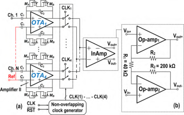
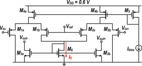
where Zout, and are output impedances of Amplifier I, and, respectively. It is inferred from (3) that the CMRR of Amplifier I can statistically be degraded by a factor of 2 compared to an amplifier with a single path from the input to the output. A high CMRR is important in brain signal amplifiers due to the presence of a strong 60 Hz power-line noise in the amplification band. If not eliminated, major degradation in the output signal-to-noise ratio (SNR) will be seen. To further improve this feature, Fig. 5 introduces the block diagram of BSA II, which is composed of an array of 4 Amplifier II circuits, a serializer, and an instrumentation amplifier (InAmp). Similar to Amplifier I, Amplifier II is realized as a fully differential RC feedback circuit incorporating 200 fF feedback and 18 pF input AC-coupled capacitors. Matching accuracy of the feedback capacitor limits the achievable CMRR. For instance, it is readily shown that for closed-loop gain of 100 and 10% mismatch of the feedback capacitor, CMRR is lower than 60 dB. The open-loop OTA within Amplifier II employs PMOS input differential-pair with NMOS cross-coupled active loads, as shown in Fig. 6(a). Having one signal path from the input to the output relaxes the mismatch considerations present in complementary signal paths used in the first design.
Fig. 5.
BSA II: (a) overall topology, including 4 Amplifier II circuits and one InAmp (b) InAmp implementation
Fig. 6.
(a) OTA schematic used in Amplifier II (b) Op-amp schematic used in InAmp
The IRNoise of the open-loop OTA is calculated to be:
| (4) |
Assuming a single-pole frequency response, it is readily proven that the noise efficiency factor (NEF [40]) reaches a lower-limit of (where n denotes the subthreshold slope factor [31]) for both OTAs used in Amplifiers I and II if no dynamic compensation techniques are employed. The use of the same closed-loop architecture as in Amplifier I indicates that the IRNoise of Amplifier II is also expressed by (2).
The InAmp, after the serializer, provides further amplification and buffering to the output. It is commonly known that isolated resistive feedback circuitry (R1 and R2) provides flexibility in the design of an InAmp and its constituent open-loop op-amps with no concern of loading on preceding circuits [41]. In addition, any variation in R1 is widely known to only contribute to the differential gain variation and will not increase common-mode to differential-mode gain (Acm−dm) [42], [43]. Therefore, the CMRR is not degraded. As for the contribution of the mismatch between the R2 resistors (R2Δ=R2 + ΔR) on CMRR, the InAmp’s Acm−dm induced by this mismatch is derived first:
| (5) |
where:
| (6) |
In deriving Eq. (5), the open-loop gains of the op-amps, Adm1 and Adm2, are assumed to be finite, while each op-amp exhibits negligible differential to common-mode gain. The common-mode gain Acm of the InAmp is almost unity. If followed by a high-CMRR amplification stage, the contribution of Acm on CMRR will be negligible. On the other hand, to reduce the impact of Acm−dm on CMRR, the op-amps need to exhibit large open-loop gain. Large open-loop gain significantly reduces the contribution of R2 mismatch on the CMRR. Ideally, if the op-amps are perfectly matched (Adm1 = Adm2), Acm−dm would become zero regardless of ΔR value.
Amplifier II and the InAmp are DC-coupled, eliminating the need for large coupling capacitors. Considering a 39-dB gain for the OTA, the expected differential input amplitude of the InAmp is less than 9 mV, which falls within the input common-mode range of InAmp (0 to VDD − 2VDS,sat where VDS,sat is the drain-source saturation voltage).
Figs. 6(a) and (b) show the transistor-level schematics of the OTA used in Amplifier II and the op-amp used in InAmp, respectively. Both amplifiers use similar topology while the devices are sized according to the performance specs needed from each circuit, namely, low noise and high transconductance for the OTA (high driving power and high voltage gain for the op-amp). Tables II and III show device sizes and operating points for the OTA and the op-amp, respectively. All transistors are biased in WI to maximize power efficiency. To achieve a maximum ECoG bandwidth of 200 Hz in the OTA and avoid out-of-band noise accumulation, a large 48 pF capacitor CL is placed differentially at the output. The input transistors operate in deep WI to maximize their gm/ID-ratio so as to reduce the IRNoise contributions of active-load devices (M2a − M2b and M3a − M3b). PMOS transistors are used in the input differential pair to have a lower flicker noise. Furthermore, the use of a PMOS input pair for the op-amp makes common-mode levels of the OTA output and the op-amp input compatible, thereby making it possible to DC-couple the two. DC-coupling eliminates the need for large decoupling capacitors as well as biasing circuitry of the op-amp inputs. The OTA bandwidth and stability are determined by its output stage where the dominant pole is located. On the other hand, the op-amp’s dominant pole is located at its first stage’s output node, as its output stage should provide high current drive capability. The op-amp is thus Miller-compensated and its bandwidth is chosen to be ≈ 800 Hz in order to accommodate 4 recording channels.
TABLE II.
Amplifier II device sizes and operating points
| Devices | W/L (μm/μm) | ID (nA) | gm/ID (V−1) |
|---|---|---|---|
| M1a-M1b | 152/0.18 | 510 | 27 |
| M2a-M2b | 12.8/20 | 255 | 20.7 |
| M3a-M3b | 12.8/20 | 255 | 20.7 |
| M4a-M4b | 0.8/25 | 27 | 16.6 |
| M5a-M5b | 16/12 | 67 | 22.9 |
| M6 | 192/1 | 1020 | 27 |
TABLE III.
Op-amp device sizes and operating points
| Devices | W/L (μm/μm) | ID (nA) | gm/ID (V−1) |
|---|---|---|---|
| M1a-M1b | 100/0.18 | 80 | 29 |
| M2a-M2b | 1/5 | 40 | 21 |
| M3a-M3b | 1/5 | 40 | 21 |
| M4a-M4b | 8/5 | 320 | 21 |
| M5a-M5b | 32/4 | 320 | 21 |
| M6 | 200/1 | 160 | 28 |
Fig. 7 shows the proposed CMFB circuit to set the output common-mode voltage of the OTA. The drain currents of transistors M4a and M4b are steered to ground or to transistor M6 depending on common-mode level of Vin. M3a and M3b mirror M6, sinking current from the OTA’s output stage, thereby adjusting the OTA common-mode level. Note that the input and the output of the CMFB are physically connected together. The CMFB output currents are expressed as:
| (7) |
where gm1,2 denotes the transconductance of M1a − M1b and M2a − M2b, W3 is channel width of M3a − M3b, and W6 is M6 width. Input transistors (M1a − M1b and M2a − M2b) should remain in saturation region for proper operation of the CMFB. Having few millivolts swing at the OTA’s output ensures that no transistor leaves saturation. Transistors M3a and M3b are designed to have long channel length, with negligible loading effect on the OTA. Their parasitic capacitances are absorbed in the OTA’s load capacitor. The simulation of the CMFB shows a current consumption of 24 nA and a common-mode phase margin of at least 35°.
Fig. 7.
CMFB circuit used in Amplifier II
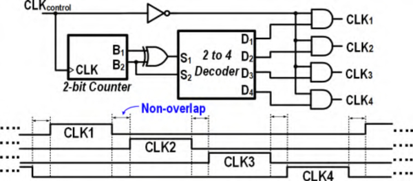
The circuitry for the serializer logic used in BSA II is presented in Fig. 8. This logic contrives i) non-overlapping clock signals for time-multiplexing, and ii) a gray-coding scheme for a 2-bit binary counter to eliminate race conditions. The serializer clock signal’s duty-cycle produces temporal spacing between clocks applied to the serializer switches (Fig. 8). A Gray-code converter is used to convert binary code to Gray code such that the counter exhibits no race condition, which could otherwise result in sparks in the 2-to-4 decoder in Fig. 8. A T-network switch is used for channel selection in this serializer to provide large input-output isolation and minimize the effects of charge-injection and clock-feedthrough.
Fig. 8.
Non-overlapping clock signals applied to serializer switches
V. Measurements
The functionality of BSAs I and II was verified by electrical and in vivo measurements. The EEG test verified the functionality of Amplifiers I and II to detect weak signals in the presence of environmental noise. BsA II was further tested in a hospital environment on a patient who underwent ECoG grid implantation over the motor cortex area. It was experimentally shown that BsA II was capable of recording signals with high output sNR and comparable performance with respect to a commercial EEG acquisition unit, while consuming orders of magnitude less power.
A. Electrical Measurements
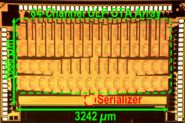
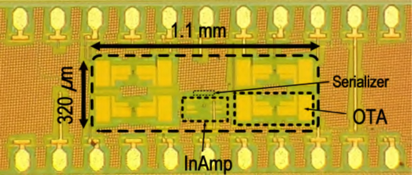
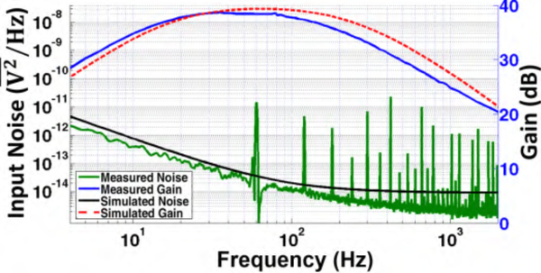
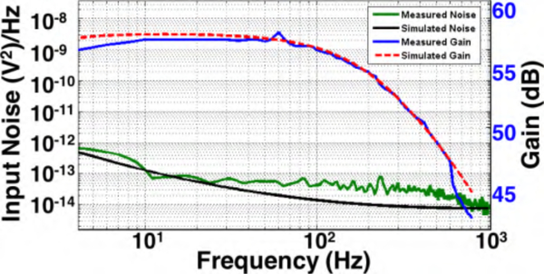
Amplifiers I and II were fabricated in 130nm and 180nm CMOS processes, occupying 0.044 mm2 / 0.052 mm2 die areas, and consuming 0.216 μW / 0.69 μW from 0.4 V / 0.6 V externally provided supply voltages, respectively. Figs. 9 and 10 show die microphotographs of BSA I and BSA II frontend circuits. The first chip (BSA I) occupies 5.45 mm2, and the second chip (BSA II) occupies 0.352 mm2 (excluding pad rings). The pad ring incorporates a 2 kV HBM ESD protection circuitry with negligible leakage current. BSA I prototype uses an off-chip buffer to drive commercial signal acquisition unit (MP150 with 12-bit ADC, Biopac Systems Inc., Goleta, CA) [23]. The overall amplification gain for the two AFEs have been measured using Agilent 33250A waveform generator and SMA attenuators, each providing 39 / 58 dB voltage gain and IRNoise of ~2.19 / 2.3 μVRMS across 12–190 Hz / 2–175 Hz of operation bandwidth, respectively (Fig. 11 and 12). Without explicit calibration scheme, the lower-cutoff frequency is not well controlled across process corners. In this work, this frequency was chosen to be smaller than the 8-Hz corner frequency of α-band with negligible effect on noise performance. Simulations show that this lower-cutoff frequency varies from 2 to 10 Hz across process corners.
Fig. 9.
Die microphotograph of BSA I with 64-channel amplifier array and serializer [23]
Fig. 10.
Die microphotograph of the BSA II with 4-channel amplifier array and serializer
Fig. 11.
Measured and simulated Amplifier I gain and noise responses. Note that the sharp peaks were due to 60 Hz harmonics on the unshielded cables [23].
Fig. 12.
Measured and simulated gain and noise responses for a single channel of BSA II
The 60 Hz interference and its harmonics were removed from the noise plot and calculations in Fig. 12. Linearity and noise measurements were done using Agilent E4448a spectrum analyzer. A low noise off-the-shelf instrumentation amplifier (AD620) was used to boost the noise level and drive the spectrum analyzer. The calculated dynamic range of the Amplifier I at 37 Hz for ~1% Total Harmonic Distortion (THD) was 58 dB. The Amplifier II harmonics for 0.2 mV input voltage at 47 Hz (which is 2 times higher than the expected neural signal amplitude) was lower than the measured noise floor, indicating linear operation. For 150 mVpp signal at 60 Hz, Amplifier I / II exhibits a CMRR greater than 60 dB / 74 dB and a PSRR greater than 58 dB / 70 dB, respectively. Table IV provides the performance summary of the designed amplifiers and comparison with prior art from academia and industry.
Table IV.
Comparison and performance summary of AFEs
| JSSC 2011 [17] |
JETCAS 2011 [19] |
TBCAS 2014 [46] |
JSSC 2015 [22] |
TBCAS 2016 [21] |
RHD2000 Intan [47] |
Amplifier I |
Amplifier II |
|
|---|---|---|---|---|---|---|---|---|
| Power (μW)† | 2.44 | 56 | 23–46 | 1.4 | 1.08 | 7.49 | 0.216 | 0.69 |
| Supply (V) | 2.8 | 3.3 | +/− 0.6 | 0.5 | 1 | 3.3 | 0.4 | 0.6 |
| Gain (dB) | 39.4 | 60 | Variable | 30 | 40 | 45.7 | 39 | 391 |
| Bandwidth (Hz) | 0.36−1.3k | 300 | 1–15k | 1–500 | 0.5–150 | 0.02–1k10 | 12–190 | 2–175 |
| IRNoise (μVRMS)7 | 3.07 | 0.5 | 132 | 1.23 | N/A3 | 2.4 | 2.19 | 2.3 |
| NEF | 3.09 | 4.4 | 7 | 3.7 | 4.525 | 4.379 | 4.65 | 7.22 |
| PEF | 26.76 | 646 | 58.56 | 6.9 | 20.436 | 639 | 11.7 | 31.3 |
| PSRR (dB) | > 80 | 69 | 39–93 | 67 | 68 | 75 | 58 | 70 |
| CMRR (dB) | > 66 | 51 | 51–97 | 88 | 82 | 82 | 60 | 74 |
| Area (mm2) | 0.13 | 868 | 12.198 | 0.025 | 0.085 | N/A | 0.044 | 0.052 |
| % THD at mVpp Input | 1% (10) | 1% (2.6) | 1% (4.5)4 | 0.4% (1) | 1% (4) | 0.8% (10) | 1% (5) | <1% (0.2) |
| Technology | 0.6 μm | 0.35 μm | 0.13 μm | 65 nm | 65 nm | N/A | 0.13 μm | 0.18 μm |
Power dissipation includes only the front-end amplifier unless otherwise stated.
58 dB for the whole AFE.
7.3 μVRMS for 300–15 kHz. 13 for 1–300 Hz μVRMS.
112 at 150 Hz.
Including ADC.
Reported for a defined single frequency. Actual value is higher.
Value calculated from reported results.
Integrated over the bandwidth.
Total chip area.
Estimated over 1 kHz bandwidth.
Bandwidth tunable from 0.02−20 kHz
B. Human Neurological Measurements
This study was approved by the Institutional Review Boards of the University of California, Irvine and the Rancho Los Amigos National Rehabilitation Center, and is considered non-significant risk. Three human subjects provided informed consent to participate. The chip was powered by a current-limited (2 mA) supply source. The hospital instruments were disconnected to avoid creation of any unwanted electrical loop. The AC-coupled connection between the electrodes and the amplifiers provides DC isolation.
1). EEG
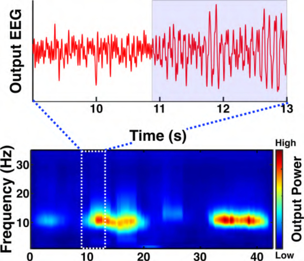
For two healthy subjects (male, 26 and 27 years old), the impedances of electrodes AFz, Cz, Pz, and Oz in the 10/10 EEG system [44] were reduced to < 3 kΩ using conductive gel. Measurements were performed on one of the subjects using Amplifier I, as follows. EEG from Cz, Pz, and Oz (all referenced to AFz) was recorded at 2353.2 Hz per channel using a data acquisition system (Biopac MP150). This sampling rate corresponds to a sampling period of ~100 μs per channel. The subject was provided verbal cues to alternate between eye opening/closing every 10 s. As a representative example, Fig. 13 shows prominent changes (~10 dB) in the power of the occipital posterior dominant α rhythm at channel Oz in both the time series and the time-frequency spectrogram during this task. This is consistent with classic neurophysiological findings [45].
Fig. 13.
Amplifier I EEG time series (top) and spectrogram (bottom) from channel Oz with 10 dB increase in the posterior dominant alpha rhythm (8–12 Hz) amplitude when the subject closed his eyes (arrow). The subject closed his eyes at 10 and 32 s and opened again at 20 and 42 s [23].
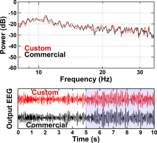
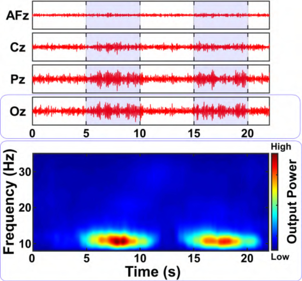
Measurements were performed on the second subject using Amplifier II, as follows. EEG from channel Oz (referenced to AFz) was split to Amplifier II as well as to a commercial bioamplifier (Biopac EEG100C) and sampled at 50 kHz. The output from both systems was downsampled to 2 kHz and filtered into the 8–35 Hz frequencies in software (see Fig. 14). The two signals exhibited a Pearson correlation coefficient of 0.89, and their envelope powers exhibited a correlation of 0.93. In addition, we recorded multiplexed EEG from electrodes AFz, Cz, Pz, and Oz (all referenced to AFz) using Amplifier II and the results after de-multiplexing in software are shown in Fig. 15. As physiologically expected, electrodes Oz and Pz exhibit larger amplitudes of the occipital posterior dominant α rhythm during the eyes-closed state.
Fig. 14.
Top: PSD of the BSA II (red) and commercial (black) bioamplifier from 30 s of EEG data. Bottom: EEG α/β-band (8–35 Hz) time-series data from channel Oz (referenced to AFz) using the BSA II (red) and commercial (black) bioamplifiers. The subject was instructed to alternate between eyes-open (white background) and eyes-closed (blue background).
Fig. 15.
BSA II EEG α/β-band (8−35 Hz) time-series data (top) and spectrogram (bottom) from channel AFz, Cz, Pz, and Oz (all referenced to AFz) as the subject was instructed to alternate between eyes-open (white background) and eyes-closed (blue background). The channel-multiplexed data from the custom designed IC were demultiplexed in software.
2). ECoG
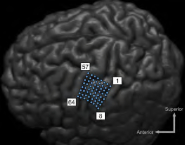
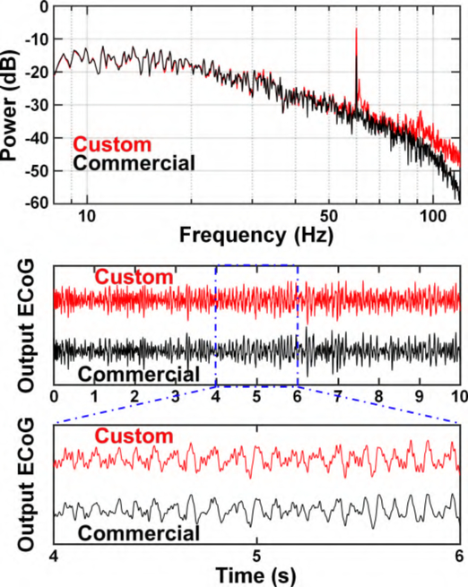
One subject (43-year-old male) undergoing ECoG implantation for epilepsy surgery evaluation participated in the study. This subject had an 8×8 grid (Ad-Tech, Racine, WI) of 2 mm-diameter electrodes (4-mm center-center spacing) implanted over the primary motor cortex. Fig. 16 shows the locations of the implanted electrodes (derived by co-registering a CT scan and MRI of the head, as in [48]). The subject completed his epilepsy monitoring procedure and was awaiting ECoG grid removal the next day. Hence, the hospital EEG system was disconnected at the time of measurement. ECoG signals were simultaneously routed to Amplifier II and a commercial EEG100C bioamplifier using unshielded cables, as shown in Fig. 17. Negligible loading effect and source impedance mismatch from EEG100C (2 MΩ input impedance) on Amplifier II is expected due to a relatively small electrodes’ impedance (<1 kΩ). ECoG electrodes’ impedance is reported to be stable over time [6], eliminating the need for constant monitoring of its value. The output from both amplifiers was recorded at 25 kHz by the MP150 system for 30 s. Note that the subject was asleep during this time and did not participate in any associated behavioral task for further verification of the amplifier array. The resulting signals were then downsampled to 2 kHz in software for further processing. The correlation coefficient between the signals from BSA II and the EEG100C was 0.99 from 8–35 Hz (covering the α and β bands), 0.94 from 35–70 Hz (low-γ band), and 0.72 from 70–120 Hz (high-γ band). Moreover, the correlation between each system’s envelope power in α/β, low-γ, and high-γ bands was 0.99, 0.99, and 0.89, respectively. This slight decrement in the high-γ band correlation between the bioamplifiers is expected since the signal power decreases with frequency and approaches the Amplifier II’s noise floor. A software notch filter was applied on the signal from 57 to 63 Hz before calculating the correlations. A representative PSD of the recorded signals across the α, β and γ bands (8–120 Hz) and 10-s output time-series of BSA II and its commercial counterpart are shown in Fig. 18, demonstrating qualitative similarities between the two. The peaks at 60 Hz for custom and commercial PSDs are caused by limited CMRR of the signal chain as well as the coupled power line interference to the unshielded interface between the analog output and the external ADC.
Fig. 16.
MRI of the patient with implanted ECoG grid over the left motor cortex. Electrodes 28 and 24 were used as the reference and ground, respectively.
Fig. 17.
In vivo ECoG measurement setup.
Fig. 18.
Top: PSD of the BSA II (red) and commercial (black) bioamplifier from 30 s of ECoG data. Middle: Filtered (8−120 Hz) time-series data from the implanted ECoG grid with the BSa II (red) and commercial (black) bioamplifier. Bottom: Zoomed-in view of the recorded ECoG.
VI. Conclusion and Future Work
Two brain signal acquisition front-ends designed in the WI region were presented. Fabricated in 130nm and 180nm CMoS processes, each amplifier within the arrays consumes 0.216 / 0.69 μW, respectively (not including buffer and InAmp). Measured IRNoise across the bandwidth was 2.19 / 2.3 μVrms corresponding to NEF of 4.65 / 7.22 and PEF of 11.7 / 31.3 [49]. Objective comparison of human in vivo EEG and ECoG measurements acquired by our custom IC and a commercial bioamplifier demonstrated that our BSAs were able to record these neural signals reliably. This suggests that the circuit architecture presented in this work can serve as the basis for a highly miniaturized and ultra-low power brain signal acquisition unit for a future fully implantable BCI system. Future work will focus on further reducing the susceptibility of the front-end to environmental noise, e.g., including an on-chip analog-to-digital converter, and incorporating the capability of large interference rejection at low supply voltages in the presence of a sensory feedback stimulation circuitry.
Acknowledgment
This research is funded by the National Science Foundation, award #1446908. The authors thank MOSIS and TowerJazz Semiconductor for chip fabrication.
Biography
 Alireza Karimi-Bidhendi (S’15) received his B.Sc. in electrical engineering alongside a minor degree in computer engineering from Sharif University of Technology, Tehran, Iran in 2013. He is working toward his PhD in electrical engineering at the University of California, Irvine. In the summer of 2015 and 2016, he was with Indie Semiconductor as an engineering intern, working on low-power oscillators and analog-to-digital converters. His research interest is analog and mixed-signal circuit design for biomedical applications. Mr. Karimi-Bidhendi is the recipient of 2013–2014 departmental fellowship and 2014 Henry Samueli fellowship.
 Omid Malekzadeh-Arasteh (S’14) received the B.S. degree in electrical engineering from Northwestern University, Evanston, IL, USA, in 2015 and is currently pursuing the Ph.D. degree in electrical engineering at University of California, Irvine, CA, USA. His research interests include analog and digital circuit design, low-power IC design and biomedical circuits for brain-computer interface applications.
 Mao-Cheng Lee received the B.S and M.S degree from National Chiao Tung University, Hsinchu, Taiwan, in 2011 and 2013, respectively. He is currently working toward the Ph.D. degree in electrical engineering and computer science at the University of California, Irvine, CA, USA. His research interests include mixed-signal and low power integrated circuit design. From 2013 to 2015 he was with Airoha Technology Corp. (Mediatek Subsidiary), Taiwan, where he was involved in the design of frequency synthesizers and calibration systems for Wi-Fi, satellite tuner and Bluetooth products.
Colin McCrimmon Biography was not available at the time of publication.
 Po T. Wang (S’09, M’14) received the B.S. degree in bioengineering from Rice University, Houston, TX in 2007, and the M.S. and Ph.D. degrees in biomedical engineering from University of California, Irvine, CA, in 2008 and 2014, respectively.
He is currently a Postdoctoral Scholar with the Department of Biomedical Engineering at University of California, Irvine, CA. His research interests include brain-computer interfaces, embedded systems, and biomedical devices and implants.
 Akshay Mahajan received the B.Tech degree in Electronics and Communications from National Institute of Technology, Hamirpur, India, in 2012 and the M.S degree in Electrical Engineering from the University of California, Irvine, USA in 2015. He is currently working in Radio Group in Broadcom Limited, San Diego, CA.
 Charles Yu Liu, PhD, MD completed his BSE in Chemical Engineering at the University of Michigan, Ann Arbor and his PhD in Chemical/Bioengineering at Rice University. The then received his MD from the Yale University School of Medicine and his neurosurgical residency at the University of Southern California affiliated hospitals. He is currently Professor of Neurosurgery, Neurology, and Biomedical Engineering at USC and Director of the USC Neurorestoration Center. He is also the Surgical Director of the USC Comprehensive Epilepsy Center and the Director of the Neuro-Recovery Programs at Rancho Los Amigos National Rehabilitation Center. His research combines the synergistic aspects of medicine and engineering to develop strategies to restore neurological function in patients with disabilities.
 Zoran Nenadic (M’06, SM’12) received the Diploma degree in control engineering from the University of Belgrade, Belgrade, Serbia, in 1995, and the M.S. and D.Sc. degrees in systems science and mathematics both from Washington University, St. Louis, MO, in 1998 and 2001, respectively. From 2001 to 2005, he was a Postdoctoral Scholar with the Division of Engineering and Applied Science at the California Institute of Technology, Pasadena. Since 2005, he has been with the Department of Biomedical Engineering, University of California, Irvine, where he is currently a Full Professor. His research interests include the area of neuroengineering, biomedical signal processing and pattern recognition, biological neural network modeling, and biomedical devices and sensors. Dr. Nenadic is the recipient of the National Science Foundation Faculty Early Career Development Award, the UC Irvine Biomedical Engineering Professor of the Year Award, and the Hiruma/Wagner Award from the Japanese Research Foundation for OptoScience and Technology.
 An H. Do, MD received his MD at the University of California, Riverside/Los Angeles Thomas Haider Biomedical Sciences Program in 2006. He completed his residency training in neurology in 2010 at the University of California, Irvine. He next undertook fellowship training in spinal cord injury medicine in a joint program at the University of California, Irvine/Long Beach Veterans Affairs Medical Center/Rancho Los Amigos National Rehabilitation Center. He is currently an assistant professor in the Department of Neurology at the University of California, Irvine. Dr. Do’s area of research is in developing and applying brain computer interfaces (BCIs) to help people with paralysis due to neurological injuries to improve or regain motor function.
 Payam Heydari (M’01, SM’09, F’17) received his B.S. and M.S. degrees (Honors) in Electrical Engineering from Sharif University of Technology in 1992 and 1995, respectively. He received his Ph.D. degree from the University of Southern California in 2001. He is currently a Full Professor of Electrical Engineering at the University of California, Irvine. Dr. Heydari’s research covers the design of terahertz/millimeter-wave/RF and analog integrated circuits. He is the (co)-author of two books, one book chapter, and more than 130 journal and conference papers. He has given Keynote Speech to IEEE GlobalSIP 2013 Symposium on Millimeter Wave Imaging and Communications, served as Invited Distinguished Speaker to the 2014 IEEE Midwest Symp. on Circuits and Systems, and gave a Tutorial at the 2017 International Solid- State Circuits Conference (ISSCC). He was a Distinguished Lecturer of the IEEE Solid-State Circuits Society from Jan. 2014 till Jan. 2016. Dr. Heydari is the recipient of the 2016–2017 UCIs School of Engineering MidCareer Excellence in Research, the 2014 Distinguished Engineering Educator Award from Orange County Engineering Council, the 2009 Business Plan Competition First Place Prize Award and Best Concept Paper Award both from Paul Merage School of Business at UC-Irvine, the 2010 Faculty of the Year Award from UC-Irvine’s Engineering Student Council (ECS), the 2009 School of Engineering Best Faculty Research Award, the 2007 IEEE Circuits and Systems Society Guillemin-Cauer Award, the 2005 IEEE Circuits and Systems Society Darlington Award, the 2005 National Science Foundation (NSF) CAREER Award, the 2005 Henry Samueli School of Engineering Teaching Excellence Award, the Best Paper Award at the 2000 IEEE Int’l Conference on Computer Design (ICCD), and the 2001 Technical Excellence Award from the Association of Professors and Scholars of Iranian Heritage (APSIH). He was recognized as the 2004 Outstanding Faculty in the EECS Department of the University of California, Irvine. His research on novel low-power multi-purpose multi-antenna RF front-ends received the Low-Power Design Contest Award at the 2008 IEEE Int’l Symposium on Low-Power Electronics and Design (ISLPED). The Office of Technology Alliances at UCI has named Dr. Heydari one of 10 Outstanding Innovators at the university. Dr. Heydari currently serves on the Technical Program Committee of the International Solid-State Circuits Conference (ISSCC). He served as the Guest Editor of IEEE Journal of Solid-State Circuits (JSSC), and Associate Editor of IEEE Trans. on Circuits and Systems - I, and served on the Technical Program Committees of Compound Semiconductor IC Symposium (CSICS), Custom Integrated Circuits Conference (CICC), and ISLPED. He served on the Technical Program Committees of and Int’l Symposium on Quality Electronic Design (ISQED), IEEE Design and Test in Europe (DATE) and International Symposium on Physical Design (ISPD). He is the director of the Nanoscale Communication IC (NCIC) Labs.
Contributor Information
Alireza Karimi-Bidhendi, Department of Electrical Engineering and Computer Science, University of California, Irvine, CA 92697 USA.
Omid Malekzadeh-Arasteh, Department of Electrical Engineering and Computer Science, University of California, Irvine, CA 92697 USA.
Mao-Cheng Lee, Department of Electrical Engineering and Computer Science, University of California, Irvine, CA 92697 USA.
Colin M. McCrimmon, Department of Biomedical Engineering, University of California, Irvine, CA 92697 USA.
Po T. Wang, Department of Biomedical Engineering, University of California, Irvine, CA 92697 USA.
Akshay Mahajan, Broadcom Ltd., San Diego, CA 91127 USA.
Charles Y. Liu, Department of Neurosurgery, University of Southern California, Los Angeles, CA 90033 USA
Zoran Nenadic, Department of Biomedical Engineering, University of California, Irvine, CA 92697 USA.
An H. Do, Department of Neurology, University of California, Irvine, CA 92697 USA
Payam Heydari, Department of Electrical Engineering and Computer Science, University of California, Irvine, CA 92697 USA.
References
- [1].W. H. Organization and I. S. C. Society, International perspectives on spinal cord injury. World Health Organization, 2013. [Google Scholar]
- [2].Do AH, Wang PT, King CE, Chun SN, and Nenadic Z, “Brain-computer interface controlled robotic gait orthosis,” J. NeuroEng. Rehabil, vol. 10, no. 111, p. 1, 2013. [DOI] [PMC free article] [PubMed] [Google Scholar]
- [3].King CE, Wang PT, McCrimmon CM, Chou CC, Do AH, and Nenadic Z, “The feasibility of a brain-computer interface functional electrical stimulation system for the restoration of overground walking after paraplegia,” J. NeuroEng. Rehabil, vol. 12, no. 1, p. 1, 2015. [DOI] [PMC free article] [PubMed] [Google Scholar]
- [4].Collinger JL, Wodlinger B, Downey JE, Wang W, Tyler-Kabara EC, Weber DJ, McMorland AJ, Velliste M, Boninger ML, and Schwartz AB, “High-performance neuroprosthetic control by an individual with tetraplegia,” The Lancet, vol. 381, no. 9866, pp. 557–564, 2013. [DOI] [PMC free article] [PubMed] [Google Scholar]
- [5].Turner J, Shain W, Szarowski D, Andersen M, Martins S, Isaacson M, and Craighead H, “Cerebral astrocyte response to micromachined silicon implants,” Exp. Neurol, vol. 156, no. 1, pp. 33–49, 1999. [DOI] [PubMed] [Google Scholar]
- [6].Sillay KA, Rutecki P, Cicora K, Worrell G, Drazkowski J, Shih JJ, Sharan AD, Morrell MJ, Williams J, and Wingeier B, “Long-term measurement of impedance in chronically implanted depth and subdural electrodes during responsive neurostimulation in humans,” Brain stimulation, vol. 6, no. 5, pp. 718–726, 2013. [DOI] [PubMed] [Google Scholar]
- [7].Wu C, Evans JJ, Skidmore C, Sperling MR, and Sharan AD, “Impedance variations over time for a closed-loop neurostimulation device: Early experience with chronically implanted electrodes,” Neuromodulation: Technology at the Neural Interface, vol. 16, no. 1, pp. 46–50, 2013. [DOI] [PubMed] [Google Scholar]
- [8].Chao ZC, Nagasaka Y, and Fujii N, “Long-term asynchronous decoding of arm motion using electrocorticographic signals in monkey,” Front. Neuroeng, vol. 3, p. 3, 2010. [DOI] [PMC free article] [PubMed] [Google Scholar]
- [9].Wang PT, King CE, McCrimmon CM, Lin JJ, Sazgar M, Hsu FP, Shaw SJ, Millet DE, Chui LA, Liu CY et al. , “Comparison of decoding resolution of standard and high-density electrocorticogram electrodes,” J. Neural Eng, vol. 13, no. 2, pp. 26016–26038, 2016. [DOI] [PMC free article] [PubMed] [Google Scholar]
- [10].Crone NE, Miglioretti DL, Gordon B, and Lesser RP, “Functional mapping of human sensorimotor cortex with electrocorticographic spectral analysis. ii. Event-related synchronization in the gamma band.” Brain, vol. 121, no. 12, pp. 2301–2315, 1998. [DOI] [PubMed] [Google Scholar]
- [11].Yanagisawa T, Hirata M, Saitoh Y, Kishima H, Matsushita K, Goto T, Fukuma R, Yokoi H, Kamitani Y, and Yoshimine T, “Electrocorticographic control of a prosthetic arm in paralyzed patients,” Ann. Neurol, vol. 71, no. 3, pp. 353–361, 2012. [DOI] [PubMed] [Google Scholar]
- [12].Kubanek J, Miller K, Ojemann J, Wolpaw J, and Schalk G, “Decoding flexion of individual fingers using electrocorticographic signals in humans,” J. Neural Eng, vol. 6, no. 6, p. 066001, 2009. [DOI] [PMC free article] [PubMed] [Google Scholar]
- [13].Rouse A, Stanslaski S, Cong P, Jensen R, Afshar P, Ullestad D, Gupta R, Molnar G, Moran D, and Denison T, “A chronic generalized bi-directional brain-machine interface,” J. Neural Eng, vol. 8, no. 3, p. 036018, 2011. [DOI] [PMC free article] [PubMed] [Google Scholar]
- [14].Afshar P, Khambhati A, Stanslaski S, Carlson D, Jensen R, Linde D, Dani S, Lazarewicz M, Cong P, Giftakis J et al. , “A translational platform for prototyping closed-loop neuromodulation systems,” Closing the Loop Around Neural Systems, pp. 367–380, 2014. [DOI] [PMC free article] [PubMed] [Google Scholar]
- [15].Swann NC, de Hemptinne C, Miocinovic S, Qasim S, Wang SS, Ziman N, Ostrem JL, San Luciano M, Galifianakis NB, and Starr PA, “Gamma oscillations in the hyperkinetic state detected with chronic human brain recordings in parkinson’s disease,” J. Neurosci, vol. 36, no. 24, pp. 6445–6458, 2016. [DOI] [PMC free article] [PubMed] [Google Scholar]
- [16].Vansteensel MJ, Pels EG, Bleichner MG, Branco MP, Denison T, Freudenburg ZV, Gosselaar P, Leinders S, Ottens TH, Van Den Boom MA et al. , “Fully implanted brain-computer interface in a locked-in patient with als,” N. Engl. J. Med, vol. 375, no. 21, pp. 2060–2066, 2016. [DOI] [PMC free article] [PubMed] [Google Scholar]
- [17].Qian C, Parramon J, and Sanchez-Sinencio E, “A micropower low-noise neural recording front-end circuit for epileptic seizure detection,” IEEE J. Solid-State Circuits, vol. 46, no. 6, pp. 1392–1405, June 2011. [Google Scholar]
- [18].Ng KA and Xu YP, “A compact, low input capacitance neural recording amplifier,” IEEE Trans. Biomed. Circuits Syst, vol. 7, no. 5, pp. 610–620, October 2013. [DOI] [PubMed] [Google Scholar]
- [19].Robinet S, Audebert P, Regis G, Zongo B, Beche J-F, Condemine C, Filipe S, and Charvet G, “A low-power 0.7 μVrms 32-channel mixed-signal circuit for ECoG recordings,” IEEE J. Emerging Sel. Top. Circuits Syst, vol. 1, no. 4, pp. 451–460, 2011. [Google Scholar]
- [20].Zhang F, Mishra A, Richardson AG, and Otis B, “A low-power ECoG/EEG processing IC with integrated multiband energy extractor,” IEEE Trans. Circuits Syst. I Regul. Pap, vol. 58, no. 9, pp. 2069–2082, 2011. [Google Scholar]
- [21].Smith W, Mogen B, Fetz E, Sathe V, and Otis B, “Exploiting electrocorticographic spectral characteristics for optimized signal chain design: A 1.08 μW analog front end with reduced ADC resolution requirements.” IEEE Trans. Biomed. Circuits Syst, 2016. [DOI] [PMC free article] [PubMed] [Google Scholar]
- [22].Muller R, Le H-P, Li W, Ledochowitsch P, Gambini S, Bjorninen T, Koralek A, Carmena JM, Maharbiz MM, Alon E et al. , “A minimally invasive 64-channel wireless μECoG implant,” IEEE J. Solid- State Circuits, vol. 50, no. 1, pp. 344–359, 2015. [Google Scholar]
- [23].Mahajan A, Bidhendi AK, Wang PT, McCrimmon CM, Liu CY, Nenadic Z, Do AH, and Heydari P, “A 64-channel ultra-low power bioelectric signal acquisition system for brain-computer interface,” in IEEE Biomed. Circuits Syst. Conf. (BioCAS), 2015, pp. 1–4. [Google Scholar]
- [24].Harrison RR, “The design of integrated circuits to observe brain activity,” Proc. IEEE, vol. 96, no. 7, pp. 1203–1216, 2008. [Google Scholar]
- [25].Enz CC and Vittoz EA, Charge-based MOS transistor modeling: the EKV model for low-power and RF IC design. John Wiley & Sons, 2006. [Google Scholar]
- [26].Shameli A and Heydari P, “Ultra-low power rfic design using moderately inverted mosfets: An analytical/experimental study,” in Radio Frequency Integrated Circuits (RFIC) Symposium, 2006 IEEE IEEE, 2006, pp. 4-pp. [Google Scholar]
- [27].Schalk G and Leuthardt EC, “Brain-computer interfaces using electrocorticographic signals,” IEEE Rev. Biomed. Eng, vol. 4, pp. 140–154, 2011. [DOI] [PubMed] [Google Scholar]
- [28].Guillory K and Normann R, “A 100-channel system for real time detection and storage of extracellular spike waveforms,” J. Neurosci. Methods, vol. 91, no. 1, pp. 21–29, 1999. [DOI] [PubMed] [Google Scholar]
- [29].Miller KJ, Sorensen LB, Ojemann JG, and Den Nijs M, “Power-law scaling in the brain surface electric potential,” PLoS Comput. Biol, vol. 5, no. 12, p. e1000609, 2009. [DOI] [PMC free article] [PubMed] [Google Scholar]
- [30].Ng KA and Xu YP, “A low-power, high CMRR neural amplifier system employing CMOS inverter-based OTAs with CMFB through supply rails,” IEEE J. Solid-State Circuits, vol. 51, no. 3, pp. 724–737, 2016. [Google Scholar]
- [31].Wang A, Calhoun BH, and Chandrakasan AP, Sub-threshold design for ultra low-power systems. New York: Springer, 2006, vol. 95. [Google Scholar]
- [32].Wang R and Harjani R, “Partial positive feedback for gain enhancement of low-power CMOS OTAs,” Analog Integrated Circuits and Signal Processing, vol. 8, no. 1, pp. 21–35, 1995. [Google Scholar]
- [33].Olsson RH, Gulari MN, and Wise KD, “Silicon neural recording arrays with on-chip electronics for in-vivo data acquisition,” in 2nd Ann. Int. IEEE-EMBS Special Topic Conf. Microtechnologies Med. and Biol. Proc. (Cat. No.02EX578), 2002, pp. 237–240. [Google Scholar]
- [34].Harrison R and Charles C, “A low-power low-noise CMOS amplifier for neural recording applications,” IEEE J. Solid-State Circuits, vol. 38, no. 6, pp. 958–965, June 2003. [Google Scholar]
- [35].Chen Z, Wang C-C, Yao H-C, and Heydari P, “A bicmos w-band 2×2 focal-plane array with on-chip antenna,” IEEE J. Solid-State Circuits, vol. 47, no. 10, pp. 2355–2371, 2012. [Google Scholar]
- [36].Gilreath L, Jain V, and Heydari P, “Design and analysis of a w-band sige direct-detection-based passive imaging receiver,” IEEE J. Solid- State Circuits, vol. 46, no. 10, pp. 2240–2252, 2011. [Google Scholar]
- [37].Avestruz A-T, Santa W, Carlson D, Jensen R, Stanslaski S, Helfenstine A, and Denison T, “A 5 μW/channel spectral analysis IC for chronic bidirectional brain-machine interfaces,” IEEE J. Solid-State Circuits, vol. 43, no. 12, pp. 3006–3024, 2008. [Google Scholar]
- [38].Yazicioglu RF, Merken P, Puers R, and Hoof CV, “A 60 μW 60 readout front-end for portable biopotential acquisition systems,” in IEEE Int. Solid-State Circuits Conf. Dig. Tech. Papers, Feb 2006, pp. 109–118. [Google Scholar]
- [39].Fan Q, Sebastiano F, Huijsing H, and Makinwa K, “A 1.8 μW 1 μV-offset capacitively-coupled chopper instrumentation amplifier in 65nm CMOS,” in Proc. Eur. Solid-State Circuits Conf. (ESSCIRC), September 2010, pp. 170–173. [Google Scholar]
- [40].Steyaert MS and Sansen WM, “A micropower low-noise monolithic instrumentation amplifier for medical purposes,” IEEE J. Solid-State Circuits, vol. 22, no. 6, pp. 1163–1168, 1987. [Google Scholar]
- [41].Horowitz P, Hill W, and Robinson I, The Art of Electronics. Cambridge university press; Cambridge, 1980, vol. 1989. [Google Scholar]
- [42].Szynowski J, “CMRR analysis of instrumentation amplifiers,” Electron. Lett, vol. 14, no. 19, pp. 547–549, 1983. [Google Scholar]
- [43].Kitchin C and Counts L, A designer’s guide to instrumentation amplifiers. Analog Devices, 2004. [Google Scholar]
- [44].Chatrian G, Lettich E, and Nelson P, “Ten percent electrode system for topographic studies of spontaneous and evoked EEG activities,” Am. J. EEG Technol, vol. 25, no. 2, pp. 83–92, 1985. [Google Scholar]
- [45].Feige B et al. , “Cortical and subcortical correlates of electroencephalographic alpha rhythm modulation,” J. Neurophysiology, vol. 93, no. 5, pp. 2864–2872, 2005. [DOI] [PubMed] [Google Scholar]
- [46].Xu J, Wu T, Liu W, and Yang Z, “A frequency shaping neural recorder with 3 pF input capacitance and 11 plus 4.5 bits dynamic range,” IEEE Trans. Biomed. Circuits Syst, vol. 8, no. 4, pp. 510–527, 2014. [DOI] [PubMed] [Google Scholar]
- [47].“Intan Technologies, RHD2000.” [Online]. Available: http://intantech.com/files/Intan_RHD2000_series_datasheet.pdf
- [48].Wang PT, King CE, Shaw SJ, Millett DE, Liu CY, Chui LA, Nenadic Z, and Do AH, “A co-registration approach for electrocorticogram electrode localization using post-implantation MRI and CT of the head,” in Neural Engineering (NER), 2013 6th Int. IEEE/EMBS Conf. on. IEEE, 2013, pp. 525–528. [Google Scholar]
- [49].Muller R, Gambini S, and Rabaey JM, “A 0.013 mm2, 5 μW, DC-coupled neural signal acquisition IC with 0.5 V supply,” IEEE J. Solid-State Circuits, vol. 47, no. 1, pp. 232–243, 2012. [Google Scholar]


