Abstract
We have used simulations and measurements to investigate the feasibility of using slanted scintillator crystal geometries as means to provide depth-of-interaction (DOI) information for a pixelated gamma ray imaging detector. The simulations were performed to estimate the fraction of scintillation light detected by the photodetector as a function of interaction location along the height of crystals with different geometries. In addition, physical measurements of the light output for these crystal geometries were obtained from individual crystals coupled to a solid state photodetector (Philips digital-SiPM DPC-3200). In agreement with previous work, we found a change in light output in the slanted region of the crystals compared to the rectangular region. The results from this study indicate the potential of using slanted crystals to gather DOI information based on light output changes as a function of the location of interaction. An examination of the measured energy spectra for the geometries evaluated here, suggests that for BGO crystals somewhere between 2 or 3 DOI bins could be implemented. Based on these results, we conceived a design for a DOI detector module that consists of two slanted crystals, each read-out by separate SiPM pixels.
Keywords: BGO, detector, scintillation crystal, optical photons, DOI, GATE, PET
I. Introduction
POSITRON Emission Tomography (PET) is commonly based on detection of the annihilation gammas through their interactions with scintillator crystals. In order to simultaneously achieve high sensitivity and high transverse spatial resolution, pixelated scintillation detectors are designed with long and narrow elements with increasingly large aspect ratios. However, designing long and narrow crystal pixels introduces two challenges. Firstly, it increases the detector parallax error [1], [2] and secondly it reduces the fraction of scintillation light available for readout by the photodetector [3]. Typically, a considerable fraction of the scintillation light never exits the crystals, getting trapped or absorbed after undergoing multiple reflections on the internal surfaces of the crystals. Furthermore, the BGO scintillation material, which is often used in PET due to its high effective atomic number Z and high attenuation coefficient [4], generates considerably less overall scintillation light than crystals made of LSO and its variants. Event positioning and detector triggering is dependent on the total amount of light collected. Therefore, it is crucial that the small amount of scintillation light produced by BGO exits the crystal in order to be detected by the light detector.
The effect of the parallax error can be reduced or eliminated if information on the depth of interaction (DOI) in the crystal was available. Ideally this DOI information should be provided without significantly compromising the fraction of scintillation light reaching the photodetector. Considerable effort over the past several years has gone into developing DOI detectors. Examples of such efforts are in [2], [5]–[20].
Previous studies with rectangular crystal pixels having different surface treatment configurations showed that crystals with five or six sides of rough treatment introduce variations in light output depending on the location of interaction of the annihilation gamma along the crystal [21]–[24]. However, in this case there is an overall degradation of light output which becomes progressively worse as the interaction occurs further up in the crystals and away from the readout side. In this work we search for a crystal geometry that offers enough difference in light output along its length while still providing a good amount of light output using BGO.
Besides material properties such as index of refraction and optical absorption length, there are several other factors affecting the probability of optical photons to exit scintillation crystals and reach the photodetector. In addition to surface treatment and the use of reflectors, one such factor is the macroscopic geometry of the crystal. Consequently, these factors pose an upper limit to the overall detector performance. In the case of scintillators coupled to photomultiplier tubes (PMTs), potential solutions to this problem have being examined before, based on the use of diffusive wrappings, optical contact agents, and crystal geometries [1], [21]–[31].
In this study, with the view of designing dense and contiguous crystal arrays coupled to solid state photodetectors with DOI capabilities for high resolution PET, we examined the performance of different scintillator geometries for BGO crystals, coupled to solid state photodetectors. Simulations of these geometries were performed by a Monte Carlo based software GATE [32], in which the crystal surfaces were defined using data acquired from physical samples measured with an atomic force microscope (AFM). To validate the simulation results, the energy spectra for different crystal geometries were obtained through measurements of individual crystals coupled to a solid state photodetector (Philips digital-SiPM sensors DPC-3200) [33]–[35]. Based on our results, a suitable geometry for a DOI detector module was proposed for polished BGO crystals.
Two previous articles examined light collection from BGO scintillators of various geometries [26], [31]. In reference [26], a Monte Carlo simulation method was implemented to study small BGO crystals with similar geometries as the crystals in this work. Measurements of the total light output and limited measurements of the dependence of the light output as a function of position along the length of the crystals were reported. In reference [31], simulations and measurements were performed for examining long (24cm) tapered BGO scintillators. As far as we know, our measurements and simulations are the first to examine in more detail the DOI effects of a non-standard geometry on small crystals for use in PET systems. This work is based on, and a substantial extension of, parts of the results and experiments found in conference record, reference [36].
II. Materials and methods
A. Simulation: Characterizing the Crystal Surface
The unified model in GATE was used to define the surfaces of all elements in the detector setup, with parameters describing surface roughness and reflectivity. In this model, a measure of surface roughness is given by the probability of an angle α for any given micro-facet (Fig.1a). This probability is proportional to the value of “sigma-alpha” (σα), given in degrees, where σα is the standard deviation of the Gaussian distribution of angles for micro-facets around the average surface normal [37].
Fig. 1.
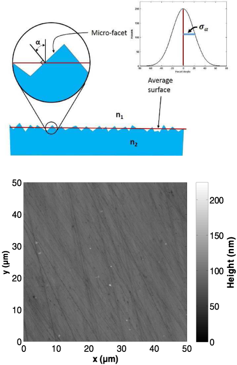
(a) Definition of micro-facets, α and σα in the Unified model used in the GATE simulations. (b) 2D view of a 50 × 50 μm2 area from a BGO polished crystal surface from an atomic force microscope. The height unit is nanometers. The information from these data was used in determining the value of σα.
To accurately describe the polished surface of a real crystal in GATE, a BGO sample crystal with dimensions 3 × 3 × 16 mm3 (Proteus Inc. Chagrin Falls, OH) was characterized in terms of surface roughness. The sample crystal had its sides cut to size on a diamond ID (inner diameter cutting edge) sawblade and then all of its faces were polished with a Cerium Oxide Polish until optically clear. Two 50 × 50 μm areas from 4 sides of the crystal were scanned (Fig. 1b) with an atomic force microscope (Bruker Dimension Icon Scanning Probe Microscope, Santa Barbara, CA). The scans were performed at ScanAsyst in Air mode using a Silicon Nitride cantilever (ScanAsyst-Air, Bruker Corporation, USA) at a frequency of 0.25 Hz and a pixel size of 0.098 × 0.098 μm.
Oscillations in the tip of the AFM caused some pixels (less than 10%) to have unreliable values. Each pixel was traced in two directions. If the values of these traces differed by a nominal amount the pixel was considered “bad” and their value was replaced using Laplace interpolation [38]. This was implemented by recursively replacing every bad pixel value by the average of its 4 nearest neighbors until the image did not change further (about 10 iterations). From these scans, the angular distribution of the surface α (Fig. 1a) from pixel to pixel in the x and y direction, was obtained. By fitting a Gaussian curve to the angular distribution, the standard deviation σα was measured to be 1.97° for the mechanically polished crystal samples in this work.
B. Simulation: Modeling the Detector Setup with GATE
To estimate the fraction of scintillation photons detected by the photodetector (SiPM) from the total generated inside a BGO crystal (optical absorption length 4.0 m), several combinations of crystal geometries were simulated using GATE. In all simulations, 4500 light photons from a point source inside the crystal at a wavelength of 480 nm were generated. The isotropic emissions assumed that the light yield of BGO has a value of ~4500 photons/511 keV [39]. Each photon was tracked starting at the emission site within the scintillator crystal, up to its absorption either by loss or via detection.
The effects of the scintillator geometry were evaluated by placing this light source at several locations along the height of the BGO crystals (Fig. 2). For every location along the height (z-direction) of the BGO crystals, a total of 1000 gammas with 511 keV were assumed to interact by the photoelectric effect. At each z-step, the x- and y-positions of the 1000 gammas were chosen at random along a transverse plane confined within the edges of the crystal. The simulations recorded the number of optical scintillation photons that reached the SiPM out of the 4500 photons produced inside the crystal for each gamma.
Fig. 2.
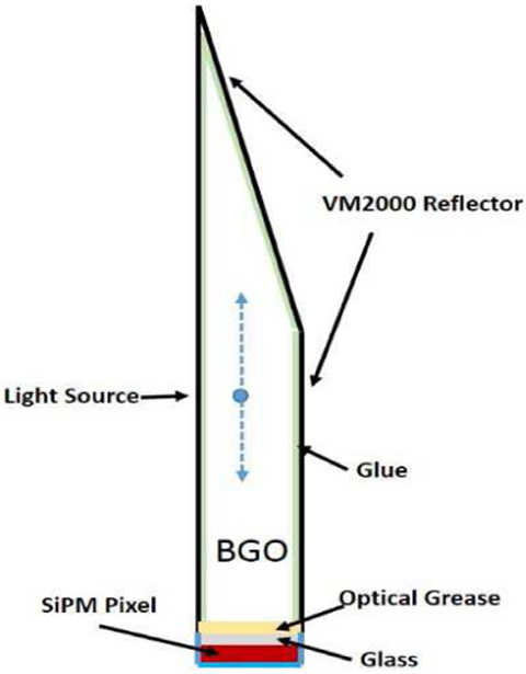
Generic detector setup for GATE simulations, showing the elements modeled in the simulation. “Light source” indicates the selected location along the crystal where a gamma-ray interacts producing 4500 scintillation photons.The simulation was run 1000 times for locations in 2mm steps along the length of the crystals. For each of the 1000 runs, the lateral position was chosen at random (within the sides of the crystal).
For the simulations, all the crystal faces were polished and the value of the parameter σα from the AFM surface characterization in section II.A was used. The refractive index and optical absorption length of the materials used in the simulation are shown in Table I.
TABLE I.
OPTICAL PARAMETERS FOR SIMULATION
| Materials | Refractive Index | Optical Absorption Length |
|---|---|---|
| BGO | 2.15 | 4 m |
| Glue(Epoxy) | 1.47 | .865 mm |
| Optical Grease | 1.56 | 8 m |
| Glass | 1.50 | 8 m |
For all geometries, the exit face of the single BGO crystal was 3 × 3 mm2 and the volume was 144 mm3. This was selected to match the dimensions of the crystals used in the physical measurements for validation (Fig. 3).
Fig. 3.
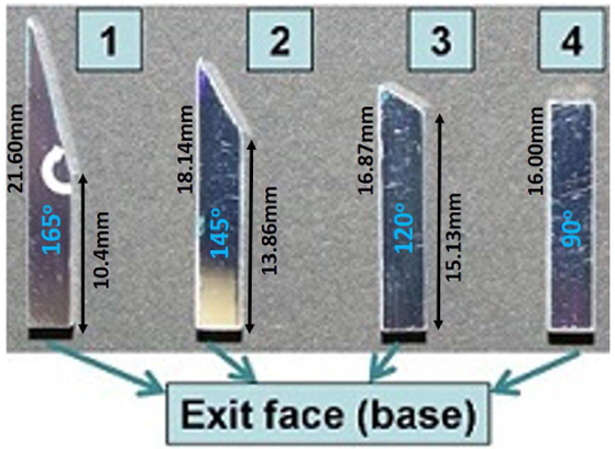
Set of four BGO crystals with dimensions. The base of all crystals was 3×3mm2 The definition of the “slant” angle is indicated by the white arrow.
C. Measurements: Evaluation of Crystals with Different Geometries
To validate the results obtained by the simulations, measurements were taken using the setup illustrated schematically in Fig. 4. The same crystal geometries as those simulated in GATE for scintillators with all the faces polished were used. Coincidence collimation was established between the BGO crystal of interest and an LYSO crystal (0.2 × 0.2 × 1.0 cm3) which was placed at a distance of 7 cm. This electronic collimation controlled the location of interaction along the length of the BGO crystal. A positron emitting source (22Na) with active volume of diameter 0.3 mm was used in all the measurements.
Fig. 4.
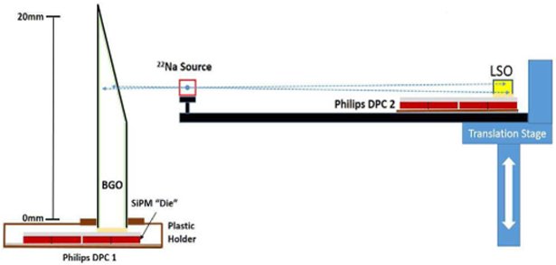
Side-view schematic of the detector setup for observing coincidences between the slanted BGO crystals and a small LSO scintillator. DPC1 and DPC2 refer to the two Philips DPC-3200 arrays used in the measurements. The arrays provide actively controled detector bias, and suppression of noisy microcells to limit dark count rate. A useful feature of the arrays is that the microcell count gives a direct measure of the number of photons detected by the sensor.
All crystals (Proteus Inc., Chagrin Falls, OH), were covered in VM2000 reflector with reflectivity of 0.98 (3M, St. Paul, MN), except at the exit face towards the photodetector. For all BGO crystals, the exit face had dimensions 3 × 3 mm2 and the volume was 144 mm3, to approximately maintain the same overall detection efficiency. These crystals were coupled with BC-630 optical grease to approximately the center of a 7.15 × 7.875 mm2 “die” of a Philips digital-photon-counting array (model:DPC-3200). Each die of the array included four pixels with each pixel consisting of 3200 microcells. The discharged cells were summed to produce the detected photon count [40]. The DPC was equipped with a digital readout board that provided the number of cells triggered per die.
Details of the operation of and parameter settings of the DPC-3200 arrays are given in [33]. Because of the low light output and long decay time of the BGO scintillator, the trigger threshold was set to 2 microcells while the validation level required was 4 microcells within a validation time of 40ns. The integration time for validated events was set to 645ns. The corresponding parameters for the DPC-3200 array reading the LYSO crystal were trigger threshold 4, validation level 8 and an integration time of 165ns. Neighbor logic was not required since only a single die was read from the two arrays.
All measurements were acquired inside an environmental chamber providing a constant temperature ~19°C for the DPC sensors. Four measurements were performed with each crystal and the same 15γ Ci 22Na point source. Assuming that the low light output of BGO was not saturating the SiPM causing non-linearities [41], the number of microcells triggered was proportional to the number of scintillation photons detected in that specific die [34]. An energy spectrum like those observed in Fig. 8 was obtained for every location of the 22Na source. The centroid of each photo-peak region was computed and plotted versus the known geometric source location.
Fig. 8.
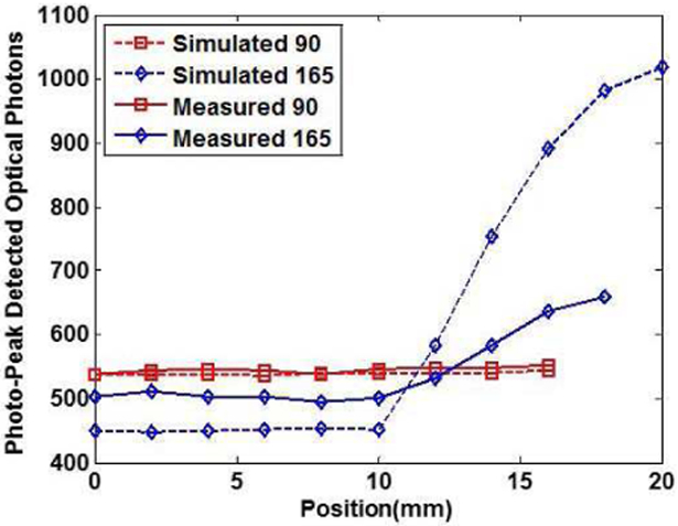
Comparison of simulation results and data for the 90 degree and 165 degree crystals. The dashed lines represent the simulation results. The simulations were normalized using the 0mm position of the 90 degree crystal as described in the text.
Each coincidence measurement was acquired for ~2 hr. To ensure repeatability of positioning the crystals on a photo-sensor die, a black plastic holder was created using a 3D printer (Bukobot, Deezmaker, Pasadena, CA). This holder tightly covered the DPC, and the crystals were placed in the holes of the holder (Fig. 4). Also, to ensure any differences in the spectra were not due to poor coupling to the DPC die or to the efficiency of a certain die, repeat measurements were acquired by re-coupling the crystals with optical grease to two different dies (two measurements per die). The variation of light output for these repeated measurements was within 1% difference (data not shown).
The exact value of the Photon Detection Efficiency (PDE) for the digital SiPM was not given by the manufacturer, but could be estimated by comparing the measured number of microcells triggered from one crystal to the number of collected photons estimated from the Monte Carlo simulations of a crystal with the same geometry. To compare the measurements with the simulations, the PDE was estimated using equation (1):
As a reference location for doing this normalization, we chose the 0 mm position from the 90° crystal, making use of the conventional rectangular crystal geometry. Based on this, the calculated value of PDE was ~45%. Another group has reported a value of 40% for this sensor [42].
In the case of the simulations, the average number of photons collected per event in equation (1) corresponds to the centroid of the collected scintillation photons. The collected scintillation photons per event are a fraction of the 4500 isotropic emissions of scintillation photons generated in a specific location along the length of the BGO crystal. This simulation was repeated 1000 times corresponding to ~1000 gamma events interacting in the scintillator.
III. Results and Discussion
A. Light Output Dependence on Scintillator Geometry
In this section we present the results from the simulations and measurements performed from crystals with all their faces mechanically polished, including the exit face. The configuration setup for the simulations is described in Fig. 2 and the configuration for the measurements is described in Fig. 4.
1). GATE Simulations:
The number of light photons exiting the crystal as a function of location of the emission is shown in Fig. 5, for the crystals with different geometries. To simplify representation of the results, the output of the simulations was normalized as described in equation 1, which assumes a PDE for the SiPM of 45%. The results show that the conventional 90° geometry has a light output that is not affected by the location of the interaction inside the crystal, in agreement with results reported by other research groups [21]. On the other hand, for the slanted crystals the simulations showed significant changes in light output compared to the rectangular crystal, especially when the interaction occurs in the slanted region of the crystal. To analyze our data, the conventional 90° geometry crystal was used as reference for the other simulations and measurements. For the 165° and 145° slanted crystals there was an up to ~60% increase in light collection at the far end of the crystals. For the 165° case, a decrease in light output was observed when interaction occurs in the rectangular region of the crystal. The 120° slanted crystal showed a ~20% increase in light output compared to the rectangular crystal over most of its length. The main source of light loss recorded in the simulations is due to absorption of light during reflections. A potential cause of the reduction in light output for the 165° -slant crystal in the rectangular region is that light generated in the lower part of the crystal and directed into the slanted region may go through more reflections leading to more light absorption compared to the 90° slant crystal.
Fig. 5.
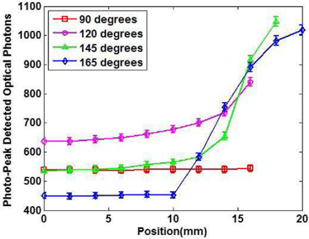
GATE simulation for polished crystals: Number of photons collected as a function of the emission location along the crystal. Position z=0 mm refers to the exit face of the crystal (see Fig. 2). The simulations were normalized to measurements by using the PDE described in equation. 1.
To obtain support for this idea, we extracted the photon his-
| (1) |
tories from GATE for a limited set of the simulation runs and examined what processes led to absorption of the undetected photons. For the same data we also ascertained the distribution of the number of reflections for each detected photon. Table II shows the percentage of photons that were indicated by GATE to be absorbed in either the epoxy or reflector during a reflection. These results are for a single point at 2mm height (rectangular region) and at 14mm height (slanted region) and represent percentages out of 4500 generated photons.
TABLE II.
PERCENTAGE OF PHOTONS ABSORBED ON REFLECTION
| 90° | 120° | 145° | 165° | |
|---|---|---|---|---|
| 2mm | 64% | 60% | 66% | 71% |
| 14mm | 66% | 54% | 58% | 53% |
The additional photons absorbed on reflection at 2mm for the 165° crystal is apparently a cause of the extra photon loss in the rectangular region.
The distributions of the number of reflections for photons eventually detected in the SiPM are shown in Fig. 6 for the 2mm positions and the 90° and 165° crystals. In both histograms, there is a cluster of events at 1, 2 and 3 reflections which represent photons directed downward towards the SiPM. As expected, in this rectangular region there are about the same number of photons in this group for both crystals (582 for the 90° and 569 for the 165° crystal). For those photons not directed towards the SiPM, the photon must incur many reflections before detection. For the 90° crystal there is a broad distribution from about 4 reflections to 18 reflections before detection. These upward directed photons produce a similar but broader distribution for the 165° crystal and in addition, this distribution is shifted and ranges from 10 to 28 reflections before detection. It is the additional required reflections for the 165° crystal that apparently accounts for the increased absorption shown in table II. An unanticipated result is that the majority of the absorption on reflection (>75%) is due to attenuation in the epoxy and not in the VM2000 reflector. This is due to the relatively high absorption coefficient for the epoxy.
Fig. 6.
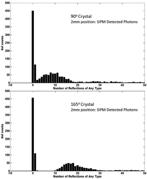
Shown are the distributions for the total number of reflections for photons that were eventually detected in the SiPM as determined by the GATE simulation for the 90° crystal (top) and the 165° crystal (bottom).
We have also examined the degree of trapping of photons by these crystals since we initially hypothesized the increased light output of slanted crystals was due to de-trapping of the light. We use the absorption of photons by the BGO as a rough measure of degree of trapping. Because of its long attenuation length (4m), trapped photons will tend to have undergone many internal reflections before being absorbed in the BGO.
If we set the σα parameter to 0° in the simulations, representing optically perfect polishing, for the 90° crystal approximately 16% of the original photons are absorbed in the BGO at both the 2mm and 14mm positions, while only a 5% are absorbed in BGO for the 165° crystal at both positions. This does represent de-trapping in the slanted crystals; however, when we use the experimentally determined value of σα (1.97 °), the percent of absorbed photons for the 90° crystal becomes only 1% at both positions. For the 165° crystal the values are ~2% at both positions, indicating little trapping. Only when the σα parameter is set to less than 0.1 ° does light trapping appear to become significant. At least as determined by this simulation model (the unified model), the depth dependence and light output difference between the rectangular crystal and the slanted ones seems to be due to the high attenuation coefficient of the epoxy and the number of reflections the photons must go through before exiting the crystals. These considerations are currently under further study.
2). Measurements:
The results of the physical measurements plotted in Fig. 7 are qualitatively consistent with the simulations in the observed trends. For the 90° geometry, the same independence of light output with respect to the depth of the interaction in the crystal is shown as reported by other research groups [21]. Matching trends as those observed in the simulations are apparent in the measurements, but the effects are far less dramatic than in the simulations. To examine our data, the measurements from the 90° crystal were taken as reference. The measured 165° and 145° crystals showed an increase in light output in the slanted region but it was only by ~25% and ~20%, respectively. The 120° crystal and the 90° crystal had similar overall light output, and in the slanted region the light output from the 120° crystal was 5% higher than in the rectangular crystal. For direct comparison, the simulations and measured data are shown on the same plot in Fig. 8, for the 90° and the 165° crystals. A possible explanation of the difference in light output between simulations and measurements is the variability in manufacturing and imperfections in processing these small crystals, as is also noted in [31]. A small difference in the cut and surface treatment of the crystals or in the reflector coupling has a potentially significant effect in the measured light output. In order to obtain a measure of this systematic error, the light output measurements in Fig. 7 were repeated using a second separate batch of crystals from the same manufacturer whose geometries and surface treatment are the same as in the crystals in Fig. 7. These measurements showed a systematically higher light output of ~12% compared to the results shown in in Fig. 7 (with a standard deviation of 3.9%), but followed the same trends, providing additional evidence to the source of variability of physical measurements.
Fig. 7.
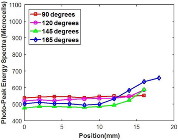
Number of microcells that fired at each location as a function of position along the crystal in measurement. Crystals with varying slant angles were evaluated using the experimental setup shown in Fig. 4. Position z=0 mm refers to the exit face of the crystal (see Fig. 2).
B. Depth of Interaction (DOI) Encoding from Energy Spectra Using Only One Crystal
From the measurements of light output with the slanted polished crystals, it was observed that the light output depends on the location of interaction of the annihilation gamma within the crystals. There was an increase in light output for locations further in the slanted region of the crystals and this effect could potentially be translated into depth of interaction information. Since the slanted crystal with 165° geometry provided the most extreme change in light output compared to all the slanted geometries evaluated here, the possibility of DOI detection was explored using this geometry.
1). GATE Simulations:
The energy spectra corresponding to the light output simulations when using the 165° slanted geometry are shown in Fig. 9. The spectra acquired anywhere in the range 0 mm to 10 mm overlap because those positions of interaction are all in the rectangular region of the crystal. From examining these energy spectra, several of the photo-peaks from different interaction depths can be clearly distinguished, yielding in principle 4 or 5 DOI bins. However, the number of possible bins in real measurements is expected to be much smaller. In the case of the physical measurements, the DOI resolution and spread of the photo-peak will be affected by the total length along which full energy deposition takes place as well as the physical width of the collimated beam in the experiment. The probability for a photoelectric effect in the first interaction in BGO at 511 keV, is approximately ~44% [43]. As a result, a large fraction of gammas will be completely stopped after two, or three interactions, thereby increasing the range of depth where the energy was deposited. This complication is not unique in this methodology, but shared also with other DOI capable detectors, such as phoswich or continuous crystal approaches [44], [45].
Fig. 9.
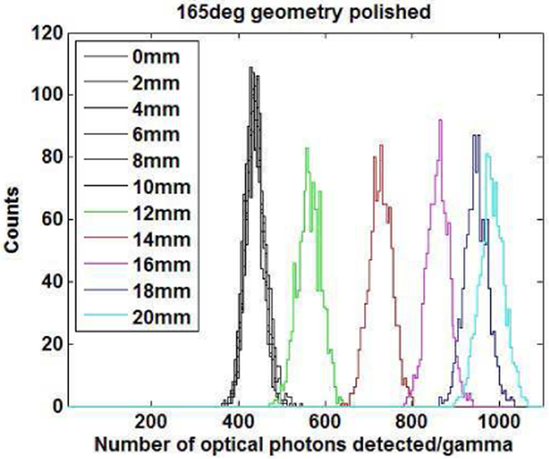
GATE simulation spectra obtained at different locations of interaction along the length of the crystal with the 165° slanted geometry (2 mm steps). The exit face of the crystal is at 0 mm.
2). Measurements:
A sample of the energy spectra at a few interaction sites is presented in Fig. 10. Spectra are shown at three different depths of interaction along the length of the crystal (10 mm, 14 mm, and 18 mm). The spectra at 10 mm was chosen to represent the spectra acquired anywhere in the range 0 mm to 10 mm. As with the simulations, the spectra in this rectangular region of the crystal overlap since the light output in this region does not change as a function of depth. An examination of the measured energy spectra, suggests that for these crystals somewhere between 2 or 3 DOI bins could be implemented based on this information.
Fig. 10.
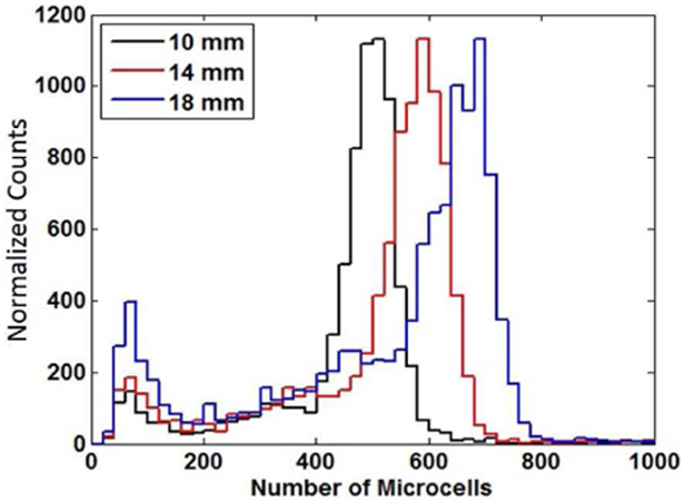
Measured energy spectra at three different depths of interaction along the length of the crystal (10 mm, 14 mm, and 18mm) corresponding to the data in Fig. 7. The maximum value of the 14mm and 18mm data have been scaled to the 10mm, to better illustrate the photoelectic peak shift.
From the energy spectra in the slanted region of the crystal (locations 10 mm to 18 mm), the energy FWHM was calculated as the spread of the number of collected scintillation photons. A linear fit was used to quantify the correlation of DOI position in the slanted region of the crystal (10mm to 18mm) and light output (Fig. 11). From the curve, the following equation was obtained:
| (2) |
Fig. 11.
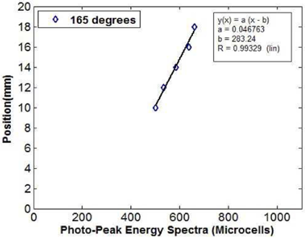
Fit to the photoelectric peak position of the measured energy spectra at 5 different depths of interaction along the length of the 165° slanted crystal.This fit resulted in the parameters shown in equation [2].
Using this equation and the value of triggered microcells at the FWHM energy limits, the corresponding positions of interaction were calculated. By subtracting the location of interaction, the DOI FWHM in units of millimeters was obtained. (Table III).
TABLE III.
METRICS OF DOI FEASIBILITY
| DOI | Spectra FWHM | DOI FWHM |
|---|---|---|
| 10 mm | 94.2 μcells | 4.4 mm |
| 12 mm | 112.0 μcells | 5.2 mm |
| 14 mm | 120.9 μcells | 5.7 mm |
| 16 mm | 124.2 μcells | 5.8 mm |
| 18 mm | 134.0 μcells | 6.3 mm |
C. Concept of Dual-readout Detector
Based on the results from the experiments performed above with the available crystals, the geometry with the largest slant angle (165°) provides the largest change in light output with position and would therefore be the best choice for a detector with DOI implementation. Following this, we conceived a dual readout detector configuration that provides DOI information as shown in Fig. 12. Two slanted crystals are positioned opposite each other and readout separately by SiPM sensors while DOI would be assigned by the magnitude of the signal in the sensor. Such a detector would have the potential to provide higher transverse spatial resolution compared to a dual ended detector that relies on crystals with roughened sides, since that approach degrades the overall amount of light that exits the crystal.
Fig. 12.

Schematic of the concept for dual-ended readout detector with two layers of interlocking slanted crystals. DOI is provided by both layers through the amount of scintillation light collected.
Like other DOI detectors, the operation of this detector is complicated by the presence of Compton scattering. In a practical detector the gamma rays would interact after traversing through an end SiPM. A photoelectric interaction in the lower portion of crystal 1 would be indistinguishable from some Compton scattered events in the upper portion of the same crystal. While some of the Compton scatters could be identified when they interact in part in crystal 2, ambiguity will remain concerning the DOI for these events. For this reason, we plan to determine the proportion of photoelectric versus Compton interaction at each crystal depth through simulation. Each of the bins based on signal magnitude, will then correspond to a probability distribution that the event occurred at a given depth along the crystal. This DOI information could be incorporated in to the reconstruction scheme. Simulation studies of such a detector are underway to both determine the probability distributions and to optimize the lengths and angles of the two crystals.
IV. CONCLUSIONS
In this work, we examined with simulations and measurements the effect of scintillator geometry on light extraction for BGO crystals coupled to the glass envelope of a SiPM. However, the effects seen in the simulations are significantly enhanced over those in the measurements, even though we obtained realistic values for the parameters used in the simulations by using AFM. Nevertheless, important information remains missing from the unified model used in this GATE simulation. It is possible that this information can account in part for the observed differences between our simulations and measurements. Some of the missing characterization refers to the description of the surfaces, for example the orientation of the micro-facets is included in this description, but not their height. Also, the reflectance properties of the surface do not take into account the photon incidence angle on the surface. The simulation indicated that most of the photon absorption is due to attenuation in the epoxy holding the reflector to the crystal. Variation in the thickness of the epoxy along the crystal could cause discrepancy between the model and the experimental results. Other factors causing differences observed between simulations and measurements relate to the geometry of the experiment set up and the imperfections of the physical crystal surfaces, reflectors and geometry. In the measurements, a collimated beam with a physical width of a few millimeters is used, rather than a defined depth in the simulations. Therefore the energy spectra from interactions around a specific location include light generated from a broader range of positions along the length of the crystal. The resulting width of the energy spectra photo-peaks are wider than with a narrower beam. In addition, due to manufacturing variability and experimental uncertainty, the crystals might have slightly different geometry and surface treatment with respect to those described in the simulations.
A recent alternative simulation model to GATE has obtained excellent results for both polished and ground rectangular LSO scintillation crystals [21], [22]. While they indicate that the unified model seemed to work well for crystals with all sides polished [21], it would be interesting if this new model could reproduce the results we have found experimentally for polished slanted BGO crystals. This could help in identifying the missing information in the unified model used in GATE.
We have examined two separate batches of crystals for the slanted-crystal studies. Within each batch the relative light outputs were consistent, but there was an overall change in the light output between batches, possibly due to differences in the surface or reflector treatment during manufacturing of the crystals. In addition, scintillation crystals can be damaged by exposure to sources of ultraviolet light. This damage might be reversed by annealing the crystals [46], [47]. However, crystals whose faces are covered by reflector material such as the crystals in this study, cannot be exposed to annealing temperatures without first removing the reflector. Careful monitoring of the surfaces of crystals at the manufacturing stage would be helpful for future studies of scintillation crystal light output.
This project explored the possibility of obtaining depth of interaction information along the length of the scintillator crystal. Both simulations and measurements showed a promising potential use of slanted crystal geometry. An examination of the measured energy spectra, suggests that for BGO crystals with 165° geometry somewhere between 2 or 3 DOI bins could be implemented based on this information, while the simulations indicate a higher number of bins (4 to 5 bins). Nevertheless, by implementing even a two bin DOI detector, it will offer a significant reduction of the positioning error of the annihilation gammas compared to detectors with no DOI estimation. In order to take into account the ambiguity posed by Compton scattering we have begun Monte Carlo simulations using detectors like that shown in Fig. 12. Tracking the interaction of gamma rays entering from one end of the detector we determine the probability that a given light output corresponds to a range of DOIs and are currently working on how to incorporate this information into the reconstruction algorithm.
Previous studies with rectangular crystals with different surface treatment configurations showed that crystals with five or six sides of rough (as-cut) treatment also provide different light output depending on the location of interaction of the annihilation gamma within the crystal [21], [23], [24]. However, in this case there was an overall degradation of light output which became progressively worse as the interaction occurred further up in the crystals and away from the readout end. Future work in this project includes conducting similar measurements using a dual-ended-readout design for a higher number of DOI bins (Fig. 12). This design will also be tested with a more extreme slanted crystal as such geometry may lead to a larger change in light output along the length of the crystal. In addition, similar measurements with other scintillators, such as LYSO, will be performed to observe if such a DOI scheme can be implemented with a high light output crystal.
ACKNOWLEDGMENTS
This work was supported by a Cota-Robles fellowship, the UCLA Foundation from a donation made by Ralph and Marjorie Crump for the UCLA Crump Institute for Molecular Imaging and NIH/NIBIB/T32 (EB002101) Research Training in Biomedical Physics. The authors would like to thank Proteus Inc. and Philips for providing the BGO crystals and digital-SiPM sensors DPC-3200, respectively, used in this study.
Contributor Information
Y. Valenciaga, Crump Institute for Molecular Imaging. She is now a Medical Physics Resident at Northwell Health (yvalenciag@northwell.edu).
D.L. Prout, Crump Institute for Molecular Imaging, David Geffen School of Medicine, University of California, Los Angeles, Los Angeles, CA 90095 USA (dprout@mednet.ucla.edu)
R. Taschereau, Crump Institute for Molecular Imaging, David Geffen School of Medicine, University of California, Los Angeles, Los Angeles, CA 90095 USA (rtaschereau@mednet.ucla.edu)
A.F. Chatziioannou, Crump Institute for Molecular Imaging, David Geffen School of Medicine, University of California, Los Angeles, Los Angeles, CA 90095 USA (archatziioann@mednet.ucla.edu)
REFERENCES
- [1].Cherry SR and Dahlbom M, PET - Physics, Instrumentation, and Scanners, Edited by Phelps ME New York: Springer, 2006. [Google Scholar]
- [2].Ito M, Hong SJ, and Lee JS, “Positron emission tomography (PET) detectors with depth-of-interaction (DOI) capability,” Biomed. Eng. Lett, vol. 1, no. 2, p. 70, May 2011. [Google Scholar]
- [3].Chatziioannou A et al. , “Coincidence measurements on detectors for microPET II: a 1 mm/sup 3/resolution PET scanner for small animal imaging,” in 2000 IEEE Nuclear Science Symposium. Conference Record (Cat. No.00CH37149), 2000, vol. 3, p. 21/1 vol.3-. [Google Scholar]
- [4].Zhang H et al. , “Performance Evaluation of PETbox: A Low Cost Bench Top Preclinical PET Scanner,” Mol. Imaging Biol, vol. 13, no. 5, pp. 949–961, Oct. 2011. [DOI] [PMC free article] [PubMed] [Google Scholar]
- [5].Lewellen TK, “Recent developments in PET detector technology,” Phys. Med. Biol, vol. 53, no. 17, pp. R287–317, Sep. 2008. [DOI] [PMC free article] [PubMed] [Google Scholar]
- [6].Hoffman EJ, Guerrero TM, Germano G, Digby WM, and Dahlbom M, “PET system calibrations and corrections for quantitative and spatially accurate images,” IEEE Trans. Nucl. Sci, vol. 36, no. 1, pp. 1108–1112, Feb. 1989. [Google Scholar]
- [7].Moses WW and Derenzo SE, “Design studies for a PET detector module using a PIN photodiode to measure depth of interaction,” IEEE Trans. Nucl. Sci, vol. 41, no. 4, pp. 1441–1445, Aug. 1994. [Google Scholar]
- [8].Murayama H, Ishibashi I, Uchida H, Omura T, and Yamashita T, “Depth encoding multicrystal detectors for PET,” IEEE Trans. Nucl. Sci, vol. 45, no. 3, pp. 1152–1157, Jun. 1998. [Google Scholar]
- [9].Wong WH, “Designing a Stratified Detection System for PET Cameras,” IEEE Trans. Nucl. Sci, vol. 33, no. 1, pp. 591–596, Feb. 1986. [Google Scholar]
- [10].Zhang N, Thompson CJ, Cayouette F, Jolly D, and Kecani S, “A prototype modular detector design for high resolution positron emission mammography imaging,” IEEE Trans. Nucl. Sci, vol. 50, no. 5, pp. 1624–1629, Oct. 2003. [Google Scholar]
- [11].Yang Y et al. , “Depth of interaction resolution measurements for a high resolution PET detector using position sensitive avalanche photodiodes,” Phys. Med. Biol, vol. 51, no. 9, p. 2131, 2006. [DOI] [PubMed] [Google Scholar]
- [12].Inadama N et al. , “8-Layer DOI Encoding of 3-Dimensional Crystal Array,” IEEE Trans. Nucl. Sci, vol. 53, no. 5, pp. 2523–2528, Oct. 2006. [Google Scholar]
- [13].Yazaki Y et al. , “Development of the X’tal Cube: A 3D Position-Sensitive Radiation Detector With All-Surface MPPC Readout,” IEEE Trans. Nucl. Sci, vol. 59, no. 2, pp. 462–468, Apr. 2012. [Google Scholar]
- [14].Shao Y, Sun X, Lan KA, Bircher C, Lou K, and Deng Z, “Development of a prototype PET scanner with depth-of-interaction measurement using solid-state photomultiplier arrays and parallel readout electronics,” Phys. Med. Biol, vol. 59, no. 5, pp. 1223–1238, Mar. 2014. [DOI] [PMC free article] [PubMed] [Google Scholar]
- [15].Du H, Yang Y, Glodo J, Wu Y, Shah K, and Cherry SR, “Continuous depth-of-interaction encoding using phosphor-coated scintillators,” Phys. Med. Biol, vol. 54, no. 6, pp. 1757–1771, Mar. 2009. [DOI] [PMC free article] [PubMed] [Google Scholar]
- [16].Ling T, Lewellen TK, and Miyaoka RS, “Depth of interaction decoding of a continuous crystal detector module,” Phys. Med. Biol, vol. 52, no. 8, pp. 2213–2228, Apr. 2007. [DOI] [PubMed] [Google Scholar]
- [17].Gu Y et al. , “Study of a high-resolution, 3D positioning cadmium zinc telluride detector for PET,” Phys. Med. Biol, vol. 56, no. 6, pp. 1563–1584, Mar. 2011. [DOI] [PMC free article] [PubMed] [Google Scholar]
- [18].Vandenbroucke A, Foudray AMK, Olcott PD, and Levin CS, “Performance characterization of a new high resolution PET scintillation detector,” Phys. Med. Biol, vol. 55, no. 19, pp. 5895–5911, Oct. 2010. [DOI] [PMC free article] [PubMed] [Google Scholar]
- [19].Seidel J, Vaquero JJ, Siegel S, Gandler WR, and Green MV, “Depth identification accuracy of a three layer phoswich PET detector module,” IEEE Trans. Nucl. Sci, vol. 46, no. 3, pp. 485–490, Jun. 1999. [Google Scholar]
- [20].Saoudi A et al. , “Investigation of depth-of-interaction by pulse shape discrimination in multicrystal detectors read out by avalanche photodiodes,” IEEE Trans. Nucl. Sci, vol. 46, no. 3, pp. 462–467, Jun. 1999. [Google Scholar]
- [21].Roncali E and Cherry SR, “Simulation of light transport in scintillators based on 3D characterization of crystal surfaces,” Phys. Med. Biol, vol. 58, no. 7, pp. 2185–2198, Apr. 2013. [DOI] [PMC free article] [PubMed] [Google Scholar]
- [22].Roncali E, Stockhoff M, and Cherry SR, “An integrated model of scintillator-reflector properties for advanced simulations of optical transport,” Phys. Med. Biol, vol. 62, no. 12, pp. 4811–4830, Jun. 2017. [DOI] [PMC free article] [PubMed] [Google Scholar]
- [23].Bircher C and Shao Y, “Investigation of crystal surface finish and geometry on single LYSO scintillator detector performance for depth-of-interaction measurement with silicon photomultipliers,” Nucl. Instrum. Methods Phys. Res. Sect. Accel. Spectrometers Detect. Assoc. Equip, vol. 693, pp. 236–243, Nov. 2012. [DOI] [PMC free article] [PubMed] [Google Scholar]
- [24].Berg E, Roncali E, Kapusta M, Du J, and Cherry SR, “A combined time-of-flight and depth-of-interaction detector for total-body positron emission tomography,” Med. Phys, vol. 43, no. 2, pp. 939–950, Feb. 2016. [DOI] [PMC free article] [PubMed] [Google Scholar]
- [25].Cherry SR, Shao Y, Tornai MP, Siegel S, Ricci AR, and Phelps ME, “Collection of scintillation light from small BGO crystals,” IEEE Trans. Nucl. Sci, vol. 42, no. 4, pp. 1058–1063, Aug. 1995. [Google Scholar]
- [26].Carrier C and Lecomte R, “Effect of geometrical modifications and crystal defects on light collection in ideal rectangular parallelepipedic BGO scintillators,” Nucl. Instrum. Methods Phys. Res. Sect. Accel. Spectrometers Detect. Assoc. Equip, vol. 294, no. 1, pp. 355–364, Sep. 1990. [Google Scholar]
- [27].Scheu S, Kaspar H, Robmann P, van der Schaaf A, and Truöl P, “Studies on wrapping materials and light collection geometries in plastic scintillators,” Nucl. Instrum. Methods Phys. Res. Sect. Accel. Spectrometers Detect. Assoc. Equip, vol. 567, no. 1, pp. 345–349, Nov. 2006. [Google Scholar]
- [28].Heinrichs U et al. , “Statistical studies on the light output and energy resolution of small LSO single crystals with different surface treatments combined with various reflector materials,” Nucl. Instrum. Methods Phys. Res. Sect. Accel. Spectrometers Detect. Assoc. Equip, vol. 486, no. 1–2, pp. 60–66, Jun. 2002. [Google Scholar]
- [29].Yang X, Downie E, Farrell T, and Peng H, “Study of light transport inside scintillation crystals for PET detectors,” Phys. Med. Biol, vol. 58, no. 7, pp. 2143–2161, Apr. 2013. [DOI] [PubMed] [Google Scholar]
- [30].Murthy K, Thompson CJ, Liu-Hinz C, and Jolly D, “A study of the light output and energy resolution of small BGO crystals,” in Nuclear Science Symposium and Medical Imaging Conference, 1994, 1994 IEEE Conference Record, 1994, vol. 3, pp. 1352–1356 vol.3. [Google Scholar]
- [31].Bea J, Gadea A, Garcia-Raffi LM, Rico J, Rubio B, and Tain JL, “Simulation of light collection in scintillators with rough surfaces,” Nucl. Instrum. Methods Phys. Res. Sect. Accel. Spectrometers Detect. Assoc. Equip, vol. 350, no. 1, pp. 184–191, Oct. 1994. [Google Scholar]
- [32].Jan S et al. , “GATE: a simulation toolkit for PET and SPECT,” Phys.Med. Biol, vol. 49, no. 19, p. 4543, 2004. [DOI] [PMC free article] [PubMed] [Google Scholar]
- [33].Schulze R, “Module-TEK Philips Digital Photon Counting,” digitalphotoncounting, 01-January-2016. [Online]. Available: http://www.digitalphotoncounting.com/wp-content/uploads/Module-TEK-User-Manual-v1_02.pdf. [Google Scholar]
- [34].Frach T, Prescher G, Degenhardt C, and Zwaans B, “The digital silicon photomultiplier #x2014; System architecture and performance evaluation,” in IEEE Nuclear Science Symposuim Medical Imaging Conference, 2010, pp. 1722–1727. [Google Scholar]
- [35].Haemisch Y, Frach T, Degenhardt C, and Thon A, “Fully Digital Arrays of Silicon Photomultipliers (dSiPM) – a Scalable Alternative to Vacuum Photomultiplier Tubes (PMT),” Phys. Procedia, vol. 37, pp. 1546–1560, Jan. 2012. [Google Scholar]
- [36].Valenciaga Y, Prout DL, and Chatziioannou AF, “Investigation of the effects of scintillator pixel shape, surface treatment and optical coupling on the performance of Si-PM based BGO detectors,” in 2013 IEEE Nuclear Science Symposium and Medical Imaging Conference (2013 NSS/MIC), 2013, pp. 1–6. [Google Scholar]
- [37].“GATE: User Manual V6.2,” OpenGateCollaboration, 01-July-2011. [Online]. Available: http://www.opengatecollaboration.org/sites/default/files/GATE_v6.2_Complete_Users_Guide.pdf. [Google Scholar]
- [38].Press W, Teukolsky S, Vetterling W, and Flannery B, Numerical Recipes: The Art of Scientific Computing, 3rd ed. Cambridge University Press, 2007. [Google Scholar]
- [39].van Eijk CWE, “Inorganic scintillators in medical imaging,” Phys. Med. Biol, vol. 47, no. 8, p. R85, 2002. [DOI] [PubMed] [Google Scholar]
- [40].“Module-TEK-User-Manual-v1_02.pdf.”.
- [41].Vinogradov S, Arodzero A, Lanza RC, and Welsch CP, “SiPM response to long and intense light pulses,” Nucl. Instrum. Methods Phys. Res. Sect. Accel. Spectrometers Detect. Assoc. Equip, vol. 787, pp. 148–152, Jul. 2015. [Google Scholar]
- [42].Lee MS and Lee JS, “Depth-of-interaction measurement in a single-layer crystal array with a single-ended readout using digital silicon photomultiplier,” Phys. Med. Biol, vol. 60, no. 16, p. 6495, 2015. [DOI] [PubMed] [Google Scholar]
- [43].Suplee C, “XCOM: Photon Cross Sections Database,” NIST, 17-September-2009. [Online]. Available: https://www.nist.gov/pml/xcom-photon-cross-sections-database. [Accessed: 23-Mar-2017].
- [44].Blinder S et al. , “Influence of depth of interaction on spatial resolution and image quality for the HRRT,” in IEEE Nuclear Science Symposium Conference Record, 2005, 2005, vol. 3, p. 5 pp.-. [Google Scholar]
- [45].Lerche CW et al. , “Dependency of Energy-, Position- and Depth of Interaction Resolution on Scintillation Crystal Coating and Geometry,” IEEE Trans. Nucl. Sci, vol. 55, no. 3, pp. 1344–1351, Jun. 2008. [Google Scholar]
- [46].Caffrey AJ, Heath RL, Ritter PD, Siclen CDV, Anderson DF, and Majewski S, “Radiation Damage Studies on BAF2 and BGO Scintillator Materials,” IEEE Trans. Nucl. Sci, vol. 33, no. 1, pp. 230–234, Feb. 1986. [Google Scholar]
- [47].Kobayashi M, Ishii M, Harada K, and Yamaga I, “Bismuth silicate Bi4Si3O12, a faster scintillator than bismuth germanate Bi4Ge3O12,” Nucl. Instrum. Methods Phys. Res. Sect. Accel. Spectrometers Detect. Assoc. Equip, vol. 372, no. 1, pp. 45–50, Mar. 1996. [Google Scholar]


