Abstract
Nanoimprint molds made of soft polymeric materials have advantages of low demolding force and low fabrication cost over Si or metal-based hard molds. However, such advantages are often sacrificed by their reduced replication fidelity associated with the low mechanical strength. In this paper, we studied replication fidelity of different UV-resin molds copied from a Si master mold via UV nanoimprint lithography (NIL) and their thermal imprinting performance into a thermoplastic polymer. Four different UV resins were studied: two were high surface energy UV resins based on tripropyleneglycol diacrylate (TPGDA resin) and polypropyleneglycol diacrylate (PPGDA resin), and the other two were commercially available, low surface energy poly-urethane acrylate (PUA resin) and fluorine-containing (MD 700) UV resins. The replication fidelity among the four UV-resins during UV nanoimprint lithograph from a Si master with sharp nanostructures was in the increasing order of (poorest) PUA resin < MD 700 < PPGDA resin < TPGDA resin (best). The results show that the high surface energy and small monomer size are keys to achieving good UV resin filling into sharp nanostructures over the viscosity of the resin solution. When the four UV-resin molds were used for thermal-NIL into a thermoplastic polymer, the replicationfidelity was in the increasing order of (poorest) MD 700 < TPGDA resin < PUA resin (best), which follows the same order of their Young’s moduli. Our results indicate that the selection of an appropriate UV resin for NIL molds requires consideration of the replication fidelities in the mold fabrication and the subsequent thermal-NIL into thermoplastic polymers.
Keywords: Nanoimprint lithography (NIL), UV-resin mold, focused ion beam milled nanostructures, replication fidelity
1. Introduction
Nanoimprint lithography (NIL) is a nanomanufacturing technology with the capability of low-cost, high throughput and large scale patterning [1, 2]. The NIL process consists of mainly two steps: molding and demolding. In the molding step, nanoscale patterns fabricated in rigid materials, e.g. silicon (Si), glass and metal, via high-end nanomachining techniques are transferred to either a thin resist layer coated on a target substrate or bulk thermoplastic polymer substrate. Depending on the method of softening/hardening the molded substrate, the process can be classified into thermal-NIL or UV-NIL. In the demolding step, the mold is released from the substrate after the substrate is hardened. Sub-10 nm features have been demonstrated by this technology [3]. However, one drawback of this technology is that the expensive rigid molds used, especially Si molds, are easily damaged during imprinting and demolding process [4].
Recently, molds made of soft polymeric materials have drawn interest over rigid molds in producing nanostructures via NIL [5, 6]. The polymeric NIL molds have usually been produced using UV-curable resins by replication from a Si master mold via UV-NIL [7]. One major advantage of using replicated UV-resin molds is their excellent demolding property for thermal-NIL, which can be attributed to their similar thermal expansion coefficient with polymer substrates and their low Young’s moduli leading to reduction in the adhesion between the UV-resin mold and the molded substrate [8]. However, the low Young’s moduli at the same time cause the mold structures to deform under high pressure and temperature conditions during thermal-NIL, resulting in a poor replication fidelity in the molded thermoplastic substrate. That can be seen in the use of PDMS molds, which is usually limited to the fabrication of microstructures [9, 10]. Thus, the Young’s moduli of UV-resin molds should be sufficiently high enough to achieve good replication fidelity during thermal-NIL but at the same time low enough to ensure low demolding force. Despite the undesired deformation during molding, the crosslinks formed in polymeric networks after UV-curing allow the replicated molds to recover to its original shape and, thus, UV-resin molds can be used many times without significant deformation [6]. Another significant advantage is that, once fabricated, the original Si master mold can be preserved and the replicated molds can be repeatedly fabricated from the original master in needs [11].
While appropriate mechanical properties of a cured UV-resin mold are important for thermal-NIL, another important requirement is to achieve good replication fidelity from the original Si mater during the fabrication of the UV-resin mold via UV-NIL. Filling of UV-resins into nanostructures of the Si master depends on many parameters such as the molecular weight of monomers, the viscosity of the UV-resin solution, surface energy of cured resin, and the nanostructure dimensions and geometries of the Si master mold [12–14]. However, the composition of a UV-resin mold which leads to good replication fidelity in thermal-NIL often shows poor filling behavior in the fabrication of the mold, in particular for extremely small nanostructures or high aspect ratio (AR) sharp nanostructures [12, 13]. Therefore, to develop UV- resin molds as a versatile molding tool for NIL, the mold filling of UV resins during the mold fabrication and the performance of replicated molds in the subsequent thermal-NIL need to be considered simultaneously.
In this work, four UV resins with different properties were used to systematically study their filling into nanostructures in the fabrication of the UV-resin molds and their performance as thermal-NIL molds. Usually, nanostructures fabricated by direct focused ion beam (FIB) milling or metal-assist FIB milling have V-shaped and sharp cross-sections due to the re-deposition nature of FIB milling [12, 15]. Therefore, we used FIB milled sharp nanostructures as model nanostructures for this study. The Si master was then replicated to four different UV-resin molds Materials and methods UV-resins via UV-NIL and the replication fidelity of the resin molds were investigated via scanning electron microscopy (SEM). Also, a thermal imprinting performance of those resin molds was studied by imprinting into cyclic olefin copolymer (COC) substrates.
2. Materials and methods
2.1. UV-resins
Four different UV-resins were used in this study: home-made tripropylene glycol diacrylate (TPGDA) UV resin, polypropyleneglycol diacrylate (PPGDA) UV resin [6, 16], commercially available poly-urethane acrylate (PUA) (PUA511RM, Minuta technology) UV resin and fluorine-containing MD 700 UV resin (Fluorolink PFPE, Solvay) [17]. The physical properties of these four resins are summarized in Table 1.
Table 1.
Physical properties of UV resins used in this study. Physical properties of TPGDA and PPGDA resin are obtained from Ref. [16]. No viscosity data of these two resin solutions is available, and their viscosity is lower than PUA and MD 700 based on our observation during experiments. Physical properties of PUA and MD 700 are obtained from supplier’s MSDS.
| UV-resin | Molecular weight of monomer (g/mol) |
Viscosity of UV resin Solution (cps) |
Young’s modulus of cured UV resin (MPa) |
Surface energy of cured UV resin (mN/m) |
|---|---|---|---|---|
| TPGDA [16] | 300 | N/A lower than PUA and MD700 |
698 | 63 |
| PPGDA [16] | 900 | N/A lower than PUA and MD 700 |
65 | 60 |
| PUA | 600–6000 [18] | 241.4 | 4771 | 24.76 |
| MD 700 | 1600 | 850 | 10.5 | 12.7 [17] |
TPGDA and PPGDA UV resins represent high surface energy UV resins, while TPGDA resin has a lower molecular weight of monomer than PPGDA resin has. A shorter chain length of TPGDA monomers leads to a shorter distance between cross-links upon curing, resulting in a higher Young’s modulus. PUA and MD 700, both of which have been used as nanoimprint molds [19–22], are representing low surface energy UV resins. Low surface energy may be problematic in filling the resin into nanostructures but is beneficial as a mold material to improve demolding without surface treatment to Si master mold [5, 20]. It should be noted that, in addition to the resin base (or monomer) that was mentioned above, a UV resin usually contains a small portion of a photoinitiator and/or a cross-linking agent. However, the properties of a resin are mostly determined by the physical and chemical properties of the base.
2.2. Fabrication of Si master molds
For the study of UV-resins filling into sharp nanostructures in a Si master mold, five nanochannels were fabricated on a Si master mold using FIB milling (Quanta 3D Dual Beam, FEI). The FIB milling was performed at a beam voltage and current of 30 kV and 10 pA, respectively, in the rectangular mode. The setting width value was 100 nm and various setting depths values (from 100 nm to 500 nm) were used. As the milling depth increased, the cross-sectional profile of the nanochannel changed from U-shaped with flat bottoms to V-shaped with sharp-tips.
For the study of UV-resin molds performance in thermal-NIL, five nanochannels with a low aspect ratio were milled in Si substrate. The milling conditions were the same as those for the Si master fabrication with sharp nanostructures. These nanochannels were connected to microchannels through a 4 μm wide and 2 μm deep inlet structure.
2.3. Fabrication of UV-resin molds and thermal imprinting
For each UV resin, five replicated molds were produced through UV-NIL from the Si master mold. UV-resin solution was first dropped on the Si master mold, then a thin polymer sheet (250 μm PET from Goodfellow, coated with an adhesion layer) was put on top of the resin solution and used as a supporting backplane. Residual resin solution and air bubbles were gently squeezed out by finger pressing. The sandwich-like structure was put in a commercial nanoimprinter (Eitre6, Obducat) and UV-NIL was performed at a UV lamp power of 1.8 W/cm2 for 20 s. After UV curing, the molded UV-resin/PET substrate was demolded from the Si master along the nanochannel direction. The schematics of the entire process steps for the fabrication of UV-resin molds and thermal-NIL into a thermoplastic substrate with the UV-resin molds are shown in Fig. S1 of the Supplementary Information.
In order to study the performance of different UV-resin molds for thermal-NIL, imprinting was performed at 160°C and 50 bar for 15 min in COC substrates (1 mm thick COC 6013 substrate, Tg=147 °C, TOPAS) with the replicated UV-resin molds having low aspect ratio patterns.
2.4. SEM imaging and ion beam cross-section cutting
For SEM imaging, a 5 nm Au/Pd layer was coated on the UV-resin molds and the imprinted COC substrates to avoid the charging effect. For cross-sectional imaging of the nanochannels in both the Si master mold and imprinted COC substrates, a thin layer of Pt was first deposited at target location using the FIB deposition mode to protect sample surface during cross-section cutting. Cross-section cutting was done using the FIB cleaning cross-section mode (30 kV, 10 pA; Quanta 3D Dual Beam, FEI). In this study, nanochannel width is defined as the width at half-depth of the channel, unless otherwise specified.
3. Results and discussion
3.1. Replication fidelity of UV-resin molds
Filling of a UV resin into nanostructures in the Si master mainly depends on the material properties of the UV resin used and the interfacial properties between the resin and the nanostructures [12, 13]. The material properties of the resin include the size (or molecular weight) of the monomer chain and the viscosity of the resin solution [4]. The most important interfacial property is surface energies of the resin and the nanostructured surface, which determines the wetting of the resin into the nanostructures. The surface energy effect (or the degree of wetting) depends on the nanostructure dimensions and geometries. Fig. 1 shows schematic of UV-resin filling into a nanostructure fabricated by direct FIB milling (Fig. 1(a) and Fig. 1(b)) and metal-assist FIB milling (Fig. 1(c) and Fig. 1(d)). Black spheres represent UV-resin monomers with a certain diameter and the dimensions of the spheres are chosen arbitrarily for the illustration purpose. As the feature size (channel width) of the FIB milled nanostructures decreases or the aspect ratio increases, the cross-sectional profile of the nanostructures becomes V-shaped (Fig. 1(b)). The smallest features that can be achieved by direct FIB milling are limited to 20 – 30 nm [23, 24]. However, this smallest feature size can further be reduced to sub-10 nm scales by FIB milling through a thick metal layer (Fig. 1(c)) [23]. Both high aspect ratio V-shaped nanostructures by direct FIB milling (Fig. 1(b)) and extremely small V-shaped nanostructures by metal-assist FIB milling (Fig. 1(d)) are hard to fill with UV-resin solution, especially for UV-resin with large sized monomers.
Fig. 1.
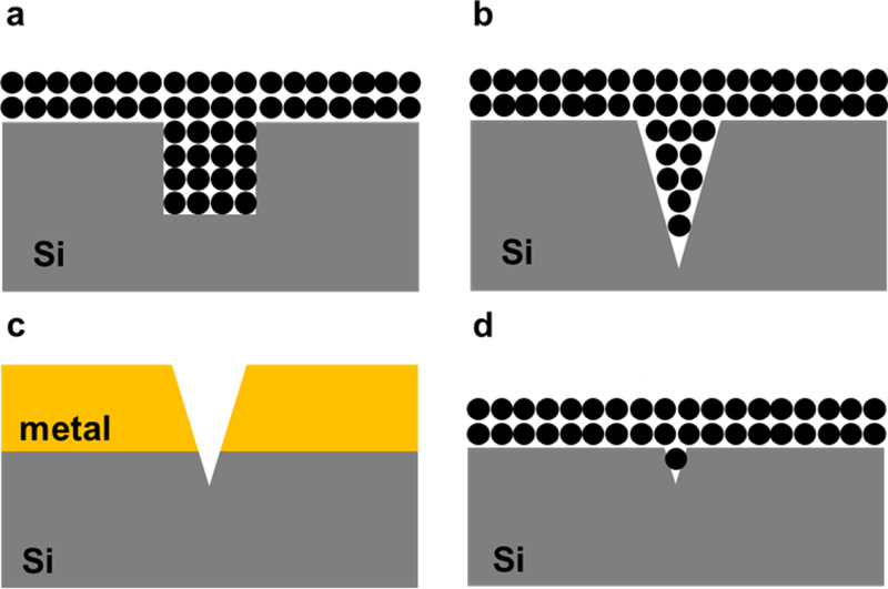
Schematic of the UV-resin filling issue for nanostructures fabricated by direct FIB milling (a, b) and small nanostructures fabricated by metal-assist FIB milling (c, d). Black spheres represent UV-resin monomers and the dimensions are chosen arbitrarily for illustration purpose. Fig. 1(a) and Fig. 1(b) have the same nanochannel width and different nanochannel depth. When milled deeper, the nanochannel cross-sectional profile becomes V-shaped. Such profile prevents complete UV-resin filling, especially for monomers with large molecular size. Metal-assist FIB milling is used to fabricate small nanostructures by coating a hundreds nanometer thick metal sacrificial layer on top of Si substrate. After removing the metal layer, the structure left on Si has small and V-shaped cross-sectional profile. UV-resin filling into such structure is much harder.
Fig. 2 shows SEM images of the cross-sectional profiles of nanochannels with different aspect ratios in the Si master used in this study. SEM images were taken with a tilt angle of 52°. For all the nanochannels, the FIB setting value for the channel width was fixed at 100 nm while the FIB setting value for the depth was varied from 100 nm to 500 nm. Even though the FIB milling was done in the rectangular mode, the cross-sectional profile of the milled nanochannels changed from a U-shape to a V-shape as the nanochannel depth increases, making it harder to fill. Fig. 2 shows that when the FIB setting value for the nanochannel depth was greater than 200 nm, the nanochannel cross-section is V-shaped with a sharp tip. Also, when the setting depth was greater than 200 nm, the sharp tip of the V-shaped cross-section has a curvature radius less than ~ 15 nm.
Fig. 2.
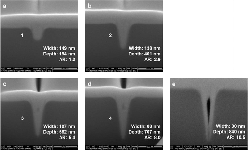
SEM images of cross-sectional profiles of nanochannels on the Si master with different aspect ratio. Nanochannels were milled by FIB rectangular mode, with 100 nm fixed setting width and setting depth ranging from 100 nm to 500 nm. When milled deeper by FIB, nanochannel cross-sectional profile changes from U-shaped to sharp tip V-shaped, which makes UV-resin solution hard to fill at the very bottom. SEM images were taken with a tilt angle of 52°.
SEM images of UV-resin molds replicated from the Si master via UV-NIL are shown in Fig. 3. For nanochannels with the lowest aspect ratio, all UV-resin molds were well replicated with good replication fidelity. For nanochannels with higher aspect ratio, the height of replicated protrusions in PUA, MD 700 and PPGDA molds were smaller than the depth of the corresponding nanochannel depth in Si master mold, which is indicative of incomplete UV resin filling. For nanochannels with higher aspect ratios, however, saw-tooth shaped defects were observed on top of the replicated protrusions in PUA and MD 700 resin molds, which is indicative of simultaneous uneven and incomplete UV resin filling into the bottom of the sharp V-shaped nanochannels. Such defects could be detrimental to the performance of imprinted products, for example, plasmon waveguides, fluorescence enhancement and biosensing devices [25]. Fig. S2 of the Supplementary Information shows SEM images of the nanochannels in PUA resin molds fabricated by UV-NIL under different pressure. The incomplete filling of UV-resin was still observed when the imprinting pressure increased up to 15 bar which is unusually high for UV- NIL. It is worth noting that, when a UV-resin mold with such defects is used as a mold for imprinting, the corresponding defects in the imprinted substrate cannot be easily detected from top-view images of SEM and optical microscopy because they occur at the very bottom of imprinted nanochannels.
Fig. 3.
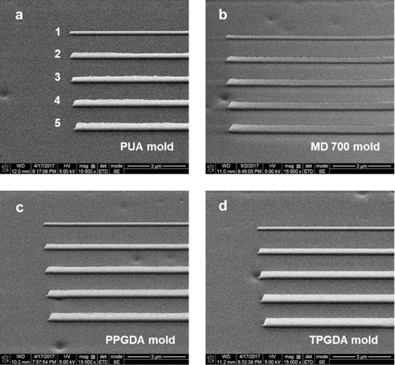
SEM images of replicated UV resin molds by UV-NIL from a Si master. Nanochannel depth increases from top to bottom as indicated by number in the image. The numbers 1–5 correspond to nanochannels 1–5 in Fig. 2. For low surface energy resins with high monomer molecular weight (PUA and MD 700), saw-tooth defects are seen for the replicated nanoprotrusions from deeper nanochannels due to uneven and incomplete resin filling. The SEM images were taken with a tilt angle of 52°.
In order to quantitatively evaluate the replication fidelity in the fabrication of UV-resin molds from the Si master, we define “UV-resin filling ratio” as the ratio of a protrusion height in the resin mold to the corresponding nanochannel depth in the Si master. The filling ratio for different UV-resins was plotted as a function of nanochannel depth (FIB setting value) in Fig. 4 (a). Overall, the UV-resin filling ratio decreases as the nanochannel depth increases, showing obviously that it is difficult to fill a UV-resin into deeper nanochannels milled by FIB. A sharp drop of the filling ratio was observed between 200 – 300 nm for all the UV resins other than TPGDA resin. This can be attributed to the fact that the cross-sectional profile of the FIB milled nanochannel changed from U-shape to V-shape with the tip curvature radius less than ~ 15 nm when the FIB setting value of the nanochannel depth was greater than 200 nm (See Fig. 1), which prevented a complete UV resin filling [13, 14]. The filling ratios among the four resins studied are in the decreasing order of TPGDA resin > PPGDA resin > PUA resin > MD 700 resin, where TPGDA resin is the best candidate for replicating sharp nanostructures by UV-NIL. The higher filling ratios of TPGDA and PPGDA resins over those of the other two resins are attributed to the combined effect of the higher surface energy and the small sizes of the resin monomers, as illustrated in Fig. 4 (b). Comparing TPGDA and PPGDA which have similar surface energies of 63 and 60 mN/m, respectively, the filling ratio of PPGDA is significantly lower than that of TPGDA, which can be attributed to TPGDA’s smaller monomer size. Comparing PUA and MD 700 resins, the viscosity of MD 700 resin is significantly higher than that of PUA resin and thus one may expect that MD 700 resin would be more difficult to fill nanostructures. However, our results show that the PUA resin has the lowest filling ratio. This indicates that the molecular size of the UV-resin monomer, together with surface energy, is a critical factor in determining the UV resin filling into nanoscale structures during UV-NIL. Larger size monomers can’t fill in the confined geometry well and UV resin solution with larger monomer size may lose its fluidity at sub- 30 nm region [14]. Even though PUA and MD 700 resins have been used as imprinting molds due to respectively the high Young’s modulus and the low surface energy [5, 20], our results indicate that they are not the appropriate candidates for UV-resin molds with sharp nanochannels with a channel width (FIB setting value) less than ~ 100 nm.
Fig. 4.
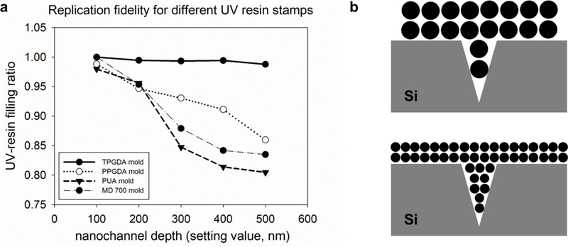
(a) UV-resin filling ratio, which represents the replication fidelity, of different UV-resin molds replicated from Si master mold during UV-NIL. In general, the UV-resin filling ratio decreases as the nanochannel depth increases. TPGDA mold with the smallest monomer size shows the highest filling ratio. (b) Schematic image of monomers with different sizes filling into sharp nanostructures, showing that UV-resins with smaller monomers show better filling into sharp nanostructures.
In addition to the incomplete filling, the saw-tooth defects are caused by uneven filling of UV resins. Saw-tooth defects occurred in PUA and MD 700 molds over PPGDA and TPGDA molds. Moreover, for the MD 700 mold with the lowest surface energy, the saw-tooth defects were seen even in the 200 nm deep (FIB setting depth) nanochannel. From our results, it can be deduced that low surface energy was the main reason for the generation of the saw-tooth defects.
Fig. S3 and S4 of the Supplementary Information show SEM images of nanochannels with ~ 200 nm and 300 nm FIB setting widths, respectively, in Si master and the replicated nanoprotrusions in PUA and TPGDA resins. The measured nanochannel widths (width at channel mouth) in the Si master were ~ 270 nm and ~ 310 nm, respectively. As the width of the nanochannel increased, the replication fidelity of the PUA resin, which was the hardest to fill nanostructures among the four resins studied, improved. The results indicate that each UV-resin has its own limit regarding the smallest feature size to achieve good replication fidelity for the resin mold fabrication, which should be an important consideration in selecting materials for resin molds and during device design.
3.2. Thermal-NIL performance of UV-resin molds
With all the replicated UV-resin molds with sharp nanostructures, we successfully replicated into COC substrates via thermal-NIL. However, since the sharp nanochannels in different UV-resin molds have different depths and different levels of saw-tooth defects, they were not suitable to be used as molds to study replication fidelity in thermal-NIL of COC substrate. Therefore, the performance of the UV-resin molds in thermal-NIL were tested using the resin molds replicated from the Si master mold with low aspect ratio nanochannels, which ensures a complete resin filling. Thermal imprinting was performed into COC substrates with the TPGDA, PUA and MD 700 resin molds. SEM images of the Si master mold and imprinted COC substrates with those resin molds are shown in Fig. 5. Top-view SEM images only showed that nanochannels were well transferred to COC substrates. However, dimensional changes were clearly seen with cross-sectional SEM images. Overall, the imprinted nanochannels on COC substrates possessed larger channel widths and smaller channel depths when compared with those of the original Si mold. The dimensional variations for the widths and depths were in a decreasing order of MD 700 (35%, 11%) > TPGDA (23%, 7%) > PUA (8%, 1%), which was consistent with the order of their Young’s modulus values. Based on our previous work, the dimensional variation of the imprinted structures from TPGDA or PPGDA resin molds is due to the mold deformation during thermal NIL process [8]. In that work, the variations of the width and depth for a 100 nm wide nanochannel imprinted in poly(methyl methacrylate) (PMMA) with a TPGDA resin mold were 22.5% and 28%, respectively. Despite such variations, the mold deformation was fully recovered after demolding because of the presence of crosslinks in the cured UV-resin [8]. For nanochannels imprinted in COC substrates in this work, larger dimensional changes in the lateral direction than those in the longitudinal direction were observed, which is different from the PMMA imprinting (imprinting conditions: 130°C, 30 bar for 5 min) results in the previous work. This may be attributed to a higher imprinting temperature for imprinting COC substrates, which results in a higher thermal stress and thus larger lateral shrinkage upon cooling. For COC substrates replicated from low Young’s modulus resin molds, more obvious deformation can be found at the nanochannel/inlet interface, which are shown in Fig. S5 of the Supplementary Information. Such defects may be attributed to stress concentration at the corner of micron-size inlet structure and could affect the device operation such as electrolyte filling or biomolecules capture in nanofluidic devices.
Fig. 5.
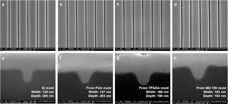
SEM images of the Si master (a, e) and imprinted COC substrates (b-c and f-h) from different UV-resin molds replicated from the Si master: top-view images (a-d) and their cross-sectional profiles (e-h). The thermal NIL performance of a UV-resin mold was determined by measuring the cross-sectional profile of the imprinted nanochannel.
4. Conclusion
In this work, we systematically studied the replication fidelity of four different UV-resin molds copied from sharp nanostructures via UV-NIL and their performance for the subsequent thermal-NIL. Production of a UV-resin mold from Si master via UV-NIL was problematic for deep nanochannels with V-shaped cross-sectional profiles milled by FIB because of incomplete resin filling. In general, UV-resin molds made from a lower molecular weight monomer and with a higher surface energy showed better replication fidelity, indicating better resin filling into the mold structures in Si. For UV resins with similar surface energy, the UV resin monomer size was found to be a critical material parameter to achieve good replication fidelity in the sub-30 nm confined region. It was difficult to quantify the relative effect of the monomer size over the other effects such as surface energy and viscosity. However, our results concluded that each UV resin has its own limitation for mold replication, which should be considered for resin selection and device design. Among the four UV resins we studied, TPGDA based resin was the best candidate for copying sharp sub-100 nm (FIB setting width) structures in Si mold. As for thermal-NIL using replicated UV-resin molds, experimental results indicated UV-resin mold with higher Young’s modulus led to less dimensional variation for imprinted patterns in COC substrates. Therefore, Young’s modulus of the cured resin is a critical material parameter to achieve good replication fidelity. Overall, this work provides insights on the material selection for UV-resin molds and the design of mold structures in Si master for thermal-NIL.
Supplementary Material
Acknowledgments
This research was supported by the P41 Center for BioModular Multiscale Systems for Precision Medicine (P41EB020594) from the National Institutes of Health.
References
- 1.Chou SY, Krauss PR, and Renstrom PJ, Imprint of sub-25 nm vias and trenches in polymers. Applied physics letters, 1995. 67(21): p. 3114–3116. [Google Scholar]
- 2.Chou SY, Krauss PR, and Renstrom PJ, Nanoimprint lithography. Journal of Vacuum Science & Technology B: Microelectronics and Nanometer Structures Processing, Measurement, and Phenomena, 1996. 14(6): p. 4129–4133. [Google Scholar]
- 3.Chou SY and Krauss PR, Imprint lithography with sub-10 nm feature size and high throughput. Microelectronic Engineering, 1997. 35(1–4): p. 237–240. [Google Scholar]
- 4.Gates BD, et al. , New approaches to nanofabrication: molding, printing, and other techniques. Chemical reviews, 2005. 105(4): p. 1171–1196. [DOI] [PubMed] [Google Scholar]
- 5.Suh D, Choi SJ, and Lee HH, Rigiflex lithography for nanostructure transfer. Advanced materials, 2005. 17(12): p. 1554–1560. [Google Scholar]
- 6.Wu J, et al. , Polymer Stamps for Imprinting Nanopatterns in Polymer Substrate. Journal of nanoscience and nanotechnology, 2015. 15(1): p. 471–474. [DOI] [PubMed] [Google Scholar]
- 7.Wolfe DB, Love JC, and Whitesides GM, Nanostructures replicated by polymer molding. Encyclopedia of Nanoscience and Nanotechnology, 2004. [Google Scholar]
- 8.Wu J, et al. , Complete plastic nanofluidic devices for DNA analysis via direct imprinting with polymer stamps. Lab on a Chip, 2011. 11(17): p. 2984–2989. [DOI] [PubMed] [Google Scholar]
- 9.Rolland JP, et al. , High-resolution soft lithography: Enabling materials for nanotechnologies. Angewandte Chemie International Edition, 2004. 43(43): p. 5796–5799. [DOI] [PubMed] [Google Scholar]
- 10.Odom TW, et al. , Improved pattern transfer in soft lithography using composite stamps. Langmuir, 2002. 18(13): p. 5314–5320. [Google Scholar]
- 11.Ahn SH and Guo LJ, Large-area roll-to-roll androll-to-plate nanoimprint lithography: a step toward high-throughput application of continuous nanoimprinting. ACS nano, 2009. 3(8): p. 2304–2310. [DOI] [PubMed] [Google Scholar]
- 12.Kannegulla A and Cheng L-J, Metal assisted focused-ion beam nanopatterning. Nanotechnology, 2016. 27(36): p. 36LT01. [DOI] [PubMed] [Google Scholar]
- 13.Nakagawa M, et al. , Size-Dependent Filling Behavior of UV-Curable Di (meth) acrylate Resins into Carbon-Coated Anodic Aluminum Oxide Pores of around 20 nm. ACS applied materials & interfaces, 2016. 8(44): p. 30628–30634. [DOI] [PubMed] [Google Scholar]
- 14.Shimazaki Y, et al. , Reduction in Viscosity of Quasi-2D-ConfinedNanoimprint Resin through the Addition of Fluorine-Containing Monomers: Shear Resonance Study. ACS applied materials & interfaces, 2013. 5(16): p. 7661–7664. [DOI] [PubMed] [Google Scholar]
- 15.Taniguchi J, et al. , Filling behavior of UV nanoimprint resin observed by using a midair structure mold. Microelectronic Engineering, 2009. 86(4): p. 676–680. [Google Scholar]
- 16.Amirsadeghi A, Developing Defect-tolerant Demolding Process in Nanoimprint Lithography. 2013. [Google Scholar]
- 17.Cho H, et al. , Replication of flexible polymer membranes with geometry-controllable nano-apertures via a hierarchical mould-based dewetting. Nature communications, 2014. 5: p. 3137. [DOI] [PubMed] [Google Scholar]
- 18.Kunwong D, Sumanochitraporn N, and Kaewpirom S, Curing behavior of a UV- curable coating based on urethane acrylate oligomer: the influence of reactive monomers. Sonklanakarin Journal of Science and Technology, 2011. 33(2): p. 201. [Google Scholar]
- 19.Finn A, et al. , High aspect ratio pattern collapse of polymeric UV-nano-imprint molds due to cleaning. Microelectronic Engineering, 2013. 110: p. 112–118. [Google Scholar]
- 20.Con C, et al. , Thermal nanoimprint lithography usingfluoropolymer mold. Microelectronic Engineering, 2012. 98: p. 246–249. [Google Scholar]
- 21.Zhang J, et al. , Low-cost fabrication of large area sub-wavelength anti-reflective structures on polymer film using a soft PUA mold. Optics express, 2014. 22(2): p. 1842–1851. [DOI] [PubMed] [Google Scholar]
- 22.Gilles S, et al. , Deformation of nanostructures on polymer molds during soft UV nanoimprint lithography. Nanotechnology, 2010. 21(24): p. 245307. [DOI] [PubMed] [Google Scholar]
- 23.Menard LD and Ramsey JM, Electrokinetically-driven transport of DNA through focused ion beam milled nanofluidic channels. Analytical chemistry, 2012. 85(2): p. 1146–1153. [DOI] [PMC free article] [PubMed] [Google Scholar]
- 24.Uba FI, et al. , Surface charge, electroosmotic flow and DNA extension in chemically modified thermoplastic nanoslits and nanochannels. Analyst, 2015. 140(1): p. 113–26. [DOI] [PMC free article] [PubMed] [Google Scholar]
- 25.Bermudez-Urena E, et al. , Coupling of individual quantum emitters to channel plasmons. Nature communications, 2015. 6: p. 7883. [DOI] [PMC free article] [PubMed] [Google Scholar]
Associated Data
This section collects any data citations, data availability statements, or supplementary materials included in this article.


