Abstract
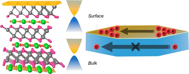
Magnetism, when combined with an unconventional electronic band structure, can give rise to forefront electronic properties such as the quantum anomalous Hall effect, axion electrodynamics, and Majorana fermions. Here we report the characterization of high-quality crystals of EuSn2P2, a new quantum material specifically designed to engender unconventional electronic states plus magnetism. EuSn2P2 has a layered, Bi2Te3-type structure. Ferromagnetic interactions dominate the Curie–Weiss susceptibility, but a transition to antiferromagnetic ordering occurs near 30 K. Neutron diffraction reveals that this is due to two-dimensional ferromagnetic spin alignment within individual Eu layers and antiferromagnetic alignment between layers—this magnetic state surrounds the Sn–P layers at low temperatures. The bulk electrical resistivity is sensitive to the magnetism. Electronic structure calculations reveal that EuSn2P2 might be a strong topological insulator, which can be a new magnetic topological quantum material (MTQM) candidate. The calculations show that surface states should be present, and they are indeed observed by angle-resolved photoelectron spectroscopy (ARPES) measurements.
Short abstract
The layered quantum material EuSn2P2 is designed, synthesized, and characterized. This new material is an ideal platform for studying the interplay of magnetism with topological electronic states.
Introduction
The design and discovery of new quantum materials with desired electronic and magnetic functionality, especially materials where quantum effects result in topological electronic properties, is a new challenge and one of the frontiers of research in materials chemistry and materials physics.1 There is a crucial need for the discovery of new materials that in particular harness the topological quantum states of matter, to increase our understanding of these newly recognized electronic states and to realize their potential in devices.2,3 In this context, topological insulators (TIs), which support fundamentally different surface (i.e., “topologically protected”) and bulk electronic states, are of particular interest.4 When additional quantum phases such as superconductivity, magnetism, or charge density waves are also present, new electronic properties can arise due to their interactions with the surface states.5,6 Currently, the study of such systems in materials physics frequently focuses on heterostructures consisting of TI/magnetic multilayers.7−10 Unfortunately, these systems cannot be widely studied due to the uncommon procedures required to make them. Thus, the design of novel magnetic topological quantum materials that are widely synthetically accessible is highly sought. Theorists have scoured the ICSD for previously reported materials that can display topological electronic properties, but the design of totally new topological quantum materials remains rare, especially for cases where the interactions of different quantum states are expected.11−16
Located at the Zintl border in the periodic table, the element Sn has moderate electronegativity, thus allowing it to participate in various types of bonding interactions. This provides flexibility in tuning the electronic properties of materials in which the electronic states of tin are dominant.17 Further, being a 5p-based element, it is expected to display the effects of spin–orbit coupling.18 Tin may be the critical elemental constituent in the topological crystalline insulator SnTe, for example, and the fabrication of Stanene thin films has been accomplished with the goal of establishing its topological electronic properties.19,20 Thus, the inclusion of tin in quantum materials is a good chemical rule when designing quantum materials with potentially unconventional electronic functionality.
A second chemical design rule for finding novel functional materials is based on symmetry and crystal structure. Experience has shown that low-dimensional materials are ideal platforms for realizing topological electronic states due to the weak interlayer interactions and subsequent partial confinement of the electronic states that is frequently present. Rhombohedral Bi2Se321 and Bi2Te3,22 and trigonal Mg3Bi2, are examples.23 The presence of elements with strong spin–orbit coupling in layers based on triangles is a common structural motif in topological quantum materials.
Finally, as a third design rule, the inclusion of magnetic lanthanide elements, if well-placed in the crystal structure, can result in the presence of ordered magnetic states that interact relatively weakly with the other electronic states present, due to the localized nature of 4f electrons.24 With appropriately selected rare earth elements at the appropriate concentration in the appropriate crystal structure, magnetically ordered states can be found at experimentally accessible temperatures. In materials with unconventional electronic structures, this allows for the interactions between magnetic and topological states to be studied.
Although nonmagnetic, the ternary Bi2Te3-type compound SrSn2As2 has been theoretically predicted to host three-dimensional Dirac states around the Fermi level.25−27 Moreover, NaSn2As2, with the same structure, is reported to be a superconductor below 1.3 K.28 Consisting of buckled SnAs honeycomb networks separated by Sr2+ or Na+, consideration of these compounds and the above materials design criteria inspired us to incorporate a magnetic rare earth element (Eu2+) between Sn-based layers with a geometry based on triangles to yield both an unconventional electronic band structure and magnetic properties in a single material.
Thus, here we report a new material by design, EuSn2P2. We report its crystallographically and magnetically ordered structures, determined via single crystal X-ray and neutron diffraction. We observe a transition to an A-type antiferromagnetic state (alternating-orientation ferromagnetic layers) near 30 K, and below that temperature significant magnetoresistance, a type-II nodal-line semimetal when spin–orbit coupling is ignored. Electronic structure calculations reveal that EuSn2P2 is an antiferromagnetic topological insulator when Hubbard (U) is included. The detailed interplay of unconventional electronic states (“band inversion”), spin–orbit coupling, and the surface states is presented theoretically. The presence of the surface states is confirmed by angle-resolved photoelectron spectroscopy (ARPES) measurements. Our new quantum material is easily grown as bulk crystals, displays magnetic ordering at accessible temperatures, and displays topological surface states, thus allowing the interactions of ferromagnetism and topological surface states to be observed in a bulk material with a simple crystal structure.
Experimental Details
Single Crystal Growth
To obtain single crystals of EuSn2P2, Eu chunks, red phosphorus, and Sn granules were placed in an alumina crucible with the molar ratio of 1.1:2:20. The crucible was sealed into an evacuated quartz tube which was then heated to 600 °C and held for 24 h followed by a 2 day heat treatment at 1050 °C. After that, the tube was cooled to 600 °C at a rate of 3 °C/h. Excess Sn was centrifuged out after reaching 600 °C, and shiny hexagonal single crystals (∼1 × 1 × 0.1 mm3) were obtained.
Structure Determination
Multiple EuSn2P2 crystals (∼60 × 60 × 5 μm3) were tested by single crystal X-ray diffraction to determine the crystal structure of the new material. The structure, consistent among all crystals, was determined using a Bruker Apex II diffractometer equipped with Mo radiation (λKα = 0.710 73 Å) at room temperature. Glycerol was used to protect the samples, which were mounted on a Kapton loop. The scan width was set to 0.5° with an exposure time of 10 s. Four different positions of the goniometer and detector were selected. Data acquisition was made via Bruker SMART software with the corrections for Lorentz and polarization effects included.29 The direct method and full-matrix least-squares on F2 procedure within the SHELXTL package were employed to solve the crystal structure.30
Physical Property Measurement
DC magnetization data were measured from 2 to 300 K using a Quantum Design Dynacool Physical Property Measurement System (PPMS), equipped with a vibrating sample magnetometer (VSM) option. The magnetic susceptibility was defined as M/H, where the applied field was 500 Oe. Field-dependent magnetization data were collected at 2 K with magnetic field up to μ0H = 9 T. The electronic transport measurements were carried out in a PPMS-9 cryostat using the four-terminal method between 1.8 and 300 K under magnetic fields up to μ0H = 9 T. Platinum wires were attached to the samples by silver epoxy to ensure ohmic contact. The normal resistivity, ρxx, was measured in the basal plane of a single crystal, simply determined by dividing the observed voltage difference by the applied current, suitably normalized by the sample dimensions. The Hall resistance, ρyx, was similarly determined by applying the magnetic field perpendicular to a single crystal basal plane and measuring the voltage within the plane perpendicular to the direction of the applied current (again suitably normalized by the sample size).
Electron Paramagnetic Resonance (EPR)
A single crystal of EuSn2P2 was stored in the glovebox before EPR measurements, and then placed in a closed sample tube. The sample tube was put into the EPR cavity. The experiment was carried out on a Bruker ER 300D spectrometer interfaced to a Bruker 1600 computer for data storage and manipulations. The spectrum was collected by sweeping the magnetic field from 0 to 5000 G.
Single Crystal Neutron Diffraction
Single crystal neutron diffraction was performed on the Four-Circle Diffractometer (HB-3A) at the High Flux Isotope Reactor (HFIR) at Oak Ridge National Laboratory (ORNL). Due to the large neutron absorption coefficient of Eu, a relatively small single crystal (∼0.8 × 0.4 × 0.02 mm3) was selected and mounted on an aluminum pin. The measurement was carried out between 4 and 50 K with an incident neutron wavelength of 1.550 Å from a bent perfect Si-220 monochromator. Absorption corrections were applied using the PLATON software.31,32 The nuclear and magnetic structure refinements were carried out using the FULLPROF refinement suite.33
Electronic Structure Calculations
The bulk electronic structure calculations for EuSn2P2 were performed by using the projector augmented wave method as implemented in the VASP package within the generalized gradient approximation (GGA) scheme.34,35 The experimental structural parameters were employed. Spin–orbit coupling was included self-consistently in some of the calculations for comparison to the expected electronic structure with SOC absent. Spin polarization using GGA+U (U = 4 eV) was employed for the magnetic models investigated.36 How f electron states are treated in DFT calculations is of interest because when considered as valence electrons then they are always found at the Fermi energy for partly filled f orbitals, which, except in very rare cases such as for heavy fermion materials,37,38 is not a realistic picture for their relative position in energy—in our calculations, the energies of the calculated Eu f electron states are tested to match with the experimental ARPES measurements. A Monkhorst–Pack 11 × 11 × 7 k-point mesh was used for the k-space integrations.39 With these settings, the calculated total energy converged to less than 0.1 meV per atom. For the surface spectral weight calculations, a semi-infinite Green’s function method, terminated by (001) surfaces, was employed. Calculations were made for Sn-, P-, and Eu-terminated (001) surfaces. The median line of the Sn bilayer is selected as the Sn-terminated surface.
Experimental Band Structure Characterization
Angle-resolved photoelectron spectroscopy (ARPES) measurements were carried out at a temperature of 10 K on the (001) surfaces of EuSn2P2 crystals cleaved in a 10–9 Pa vacuum. Linearly (s and p) polarized light with photon energies in the range 50–120 eV was used. Experiments were performed at the Electron Spectro-Microscopy (ESM) beamline of the National Synchrotron Light Source (NSLS-II). The photoemitted electrons were collected from a ±15° cone by a Scienta DA30 instrument and analyzed with angular and energy resolutions of <0.2° and 15 meV, respectively. Core level spectra using 300 eV photons showed presence of no elements other than Sn, Eu, and P in the material. Potassium adsorption, commonly used to fill a material’s bands with additional electrons to increase the Fermi Level at the surface of a sample, resulted in surface deterioration in the case of EuSn2P2 and no noticeable Fermi level shift.
Safety Statement
No unexpected or unusually high safety hazards were encountered.
Results and Discussion
Crystal Structure
The single crystals of EuSn2P2 are hexagonal plates, as shown in Figure 1A, with the rhombohedral c-axis perpendicular to the plates (thus the plates are (001) or “basal” planes). The results from single crystal X-ray diffraction reveal that EuSn2P2 crystallizes in a rhombohedral lattice with the space group R3̅m, in analogy to Bi2Te3, which is a well-known topological insulator. As shown in Figure 1B, each Eu atom, surrounded by six P atoms, forms a trigonal prism. The Eu layers are separated by two Sn@P3 triangular pyramid layers connected by weak Sn–Sn bonds. An inversion center exists in the center of the unit cell. The layered features of EuSn2P2, and its in-plane and honeycomb Sn structure viewed along c-axis are presented in Figure 1C,D, respectively. The crystallographic data, including atomic positions, site occupancies, and equivalent isotropic thermal displacement parameters, are listed in Tables 1 and 2. The refined anisotropic displacement parameters are shown in Table S1.
Figure 1.
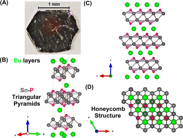
Crystal structure of EuSn2P2 from different viewpoints, where the green, gray, and red balls represent Eu, Sn, and P atoms, respectively. (A) Single crystal picture of EuSn2P2. (B, C) Layered characteristic structure of EuSn2P2 (looking perpendicular to the c-axis). (D) Emphasizing the honeycomb character of the double Sn layers in the basal plane and the triangular planes of Eu (looking parallel to the c-axis).
Table 1. Single Crystal Structure Refinement for EuSn2P2 at 293 (2) K.
| refined formula | EuSn2P2 |
| F.W. (g/mol) | 451.28 |
| space group; Z | R3̅m; 3 |
| a (Å) | 4.097 (1) |
| c (Å) | 26.162 (5) |
| V (Å3) | 380.24 (13) |
| extinction coefficient | 0.0000 (1) |
| θ range (deg) | 2.335–33.171 |
| no. reflections; Rint | 2229; 0.0191 |
| no. independent reflections | 227 |
| no. parameters | 10 |
| R1: ωR2 (I > 2δ(I)) | 0.0154; 0.0363 |
| goodness of fit | 1.121 |
| diffraction peak and hole (e–/Å3) | 2.481; −0.617 |
Table 2. Atomic Coordinates and Equivalent Isotropic Displacement Parameters for EuSn2P2 at 293 Ka.
| atom | Wyck. | occ. | x | y | z | Ueq |
|---|---|---|---|---|---|---|
| Eu1 | 3a | 1 | 0 | 0 | 0 | 0.0088 (1) |
| Sn2 | 6c | 1 | 0 | 0 | 0.2112 (1) | 0.0117 (1) |
| P3 | 6c | 1 | 0 | 0 | 0.4053 (1) | 0.0087 (3) |
Ueq is defined as one-third of the trace of the orthogonalized Uij tensor (Å2).
Magnetic Characterization
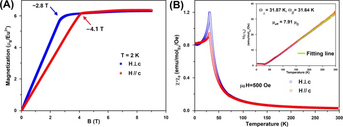
To get insight into the magnetic properties of EuSn2P2, we performed field-dependent magnetization measurements at 2 K with applied magnetic fields parallel and perpendicular to the c-axis. The results are shown in Figure 2A. The field-dependent behavior is characteristic of that of a ferromagnetic material—the magnetic moment of EuSn2P2 saturates at ∼2.8 T for applied fields perpendicular to the c-axis and ∼4.1 T for fields parallel to the c-axis. Accordingly, a strong anisotropy of magnetization is observed, with the easy axis in the basal plane, perpendicular to the c-axis. The saturated magnetizations are ∼6.0 μB/Eu for both orientations.
Figure 2.
Field-dependent, direction-dependent, and temperature-dependent magnetic properties of EuSn2P2. (A) Field-dependent magnetization for the two crystal orientations measured at 2 K where red balls and blue squares represent magnetic field parallel and perpendicular to the c-axis, respectively. (B) Magnetic susceptibility as a function of temperature measured in an external field of μ0H = 500 Oe, both perpendicular (blue) and parallel (red) to the c-axis. The inset shows the temperature-dependent inverse susceptibility, measured for different sample orientations. The green line is the Curie–Weiss fit to the high-temperature data.
The temperature-dependent magnetic susceptibility was measured
under an external field of 500 Oe from 2 to 300 K. A transition to
an antiferromagnetic state (i.e., TN)
is seen at around 30 K. The larger magnetic susceptibility in the
perpendicular field also indicates the anisotropic ordered magnetism
in EuSn2P2, i.e., that ferromagnetic ordering
is preferred within the ab-plane rather than along
the c-axis. At temperatures higher than 30 K, classic
Curie–Weiss behavior is observed.40 The effective moment and Curie–Weiss (CW) temperatures Θ⊥ and Θ// were fitted from 150 to 300
K by using the Curie–Weiss formula χ = χ0 +  where χ0 is the temperature-independent
part of the magnetic susceptibility, NA is Avogadro’s number, kB is the
Boltzmann constant, μeff is the effective moment,
and ΘCW is the Curie–Weiss temperature. The Curie–Weiss temperatures in perpendicular and parallel
fields are 31.8(1) and 31.6(1) K, within error of each other, while
the average effective moment is 7.91(3) μB/Eu. The
magnetic characteristics above TN are
essentially isotropic.
Electron Paramagnetic Resonance (EPR)
The magnetism
observed is consistent with the presence of magnetic Eu2+ in our material, but to further confirm the electronic state of
Eu in EuSn2P2, we performed electron paramagnetic
resonance measurements. The obtained data are shown in Figure 3 as the first derivative of
the absorption data. We observe a sin-function-like strong broad curve
when the applied magnetic field is swept to 2400 G, reaching its maximum
around 3200 G. The intensity subsequently drops to zero at 3530 G,
which indicates the applied field of the strongest absorption, and
continuously becomes more negative, to ∼−6000 (in arbitrary
units) at ∼3800 Oe, returning to zero intensity beyond 5000
Oe. The asymmetric line shape is as is usually observed in metals
due to the skin effect caused by the small size of the single crystal
used compared with the skin depth. According to the principal EPR
equation, ΔE = hν = gμBB0 where
ΔE is the splitting energy, h is Planck’s constant, ν is the frequency of the microwave
used, which is 9481 MHz, g is the Landé g-factor, μB is the Bohr magneton, and B0 is the applied magnetic field of the strongest
absorption, we obtain the Landé g-factor of
1.9184. Based on μeff = g μB and the g-factor obtained from the EPR data,
we obtain μeff = 7.61 μB, which
is within error of the effective
moment obtained from the temperature-dependent magnetic susceptibility
(7.91 μB).41 Therefore,
we find that, for Eu in EuSn2P2, J = 7/2 and that the Eu ground state is 8S7/2, i.e., that Eu2+ is the primary valence state for Eu.
Figure 3.
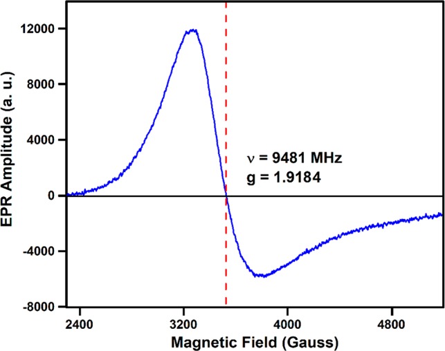
Characterization of the Eu spin state at ambient temperature and pressure in EuSn2P2. Room temperature electron paramagnetic resonance (EPR) measurement with applied magnetic field from 2300 to 5200 G.
Magnetic Structure
To better understand the magnetic
properties of our new quantum material, we performed single crystal
neutron diffraction on EuSn2P2. Antiferromagnetic
order onsets at 30 K, as indicated by observing extra Bragg peaks
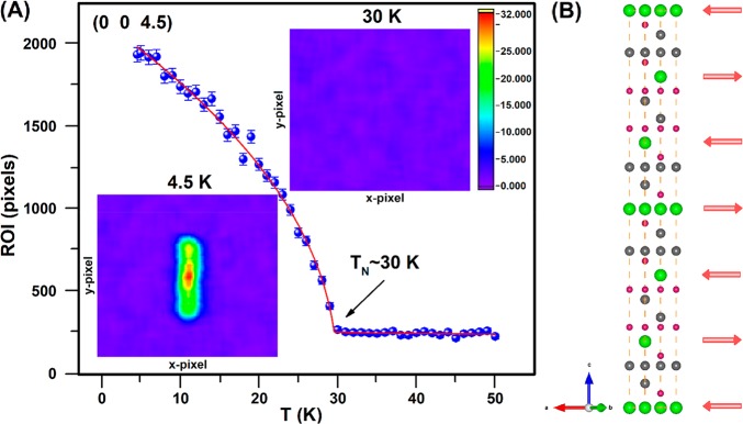
with a propagation vector of (0 0 1.5). The ordering parameter was
measured at (0 0 4.5) in reciprocal space (see Figure 4A) and indicates that TN ∼ 30 K by determination of the intersection of a linear
fitting regime (30–50 K) and a two-term power law fit at low
temperatures with  where A, pl, pu, and xc are all constants.33 The magnetic
structure is determined by modeling
the magnetic reflections collected at 4.5 K. The lattice parameters
(a = 4.069(2) Å, c = 25.935(9)
Å) at 4.5 K are smaller than those determined by single crystal
X-ray diffraction (a = 4.097(1) Å, c = 26.162(5) Å) at room temperature due to thermal contraction.
Refining the nuclear reflections collected at 4.5 K yields RF = 9.15% and RF2 = 17.69%. The magnetic structure refinement reaches
the best fit (RF = 6.71% and RF2 = 12.7%) with the magnetic moment of 5.65
(3) μB/Eu oriented in the ab-plane
at 4.5 K (see Figure 4B), consistent with the field-dependent magnetization measurements.
As shown in Figure 4B, the result is ferromagnetic Eu layers antiferromagnetically coupled
with their nearest neighbor layers leading to A-type antiferromagnetism
for EuSn2P2. The inset of Figure 4A illustrates the neutron diffraction intensity
maps at both 30 and 4.5 K, showing the magnetic peak at (0 0 4.5).
Figure 4.
Magnetic structure of EuSn2P2. (A) (main panel) Temperature-dependence of the magnetic scattering. The pixel number is for the selected region of interest (enclosed in the purple rectangle insets). The data indicate that TN ∼ 30 K, resulting from the fit of the red curves to the data. (insets, top right) Magnetic signal intensity map at 30.0 K for the reciprocal lattice plane (0 0 4.5). (insets, bottom left) Magnetic signal intensity map at 4.5 K for the reciprocal lattice plane (0 0 4.5). (B) Magnetic unit cell of EuSn2P2. The red arrows indicate the orientation of magnetic moments for each layer of Eu atoms.
Charge Transport
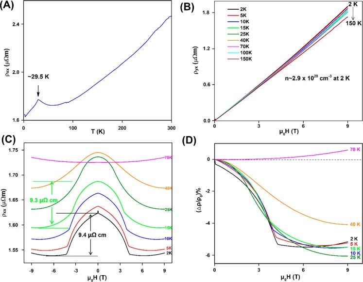
The transport of electrical charge in materials where interactions between different states may be present is of interest. The temperature-dependent resistivity for a single crystal of EuSn2P2, measured in the (001) plane, is thus shown in Figure 5A. Decreasing resistivity with decreasing temperature, i.e., metallic behavior, is observed. The charge transport is sensitive to the magnetic state of the system: ρxx (the resistivity in the x direction with the electric field applied along the x direction; x and y directions are in the plane of the layers, while z is perpendicular to the layers) shows a drop below the Neel temperature (∼30 K). The in-plane resistivity ρxx increases slightly at temperatures above the magnetic ordering temperature, starting near 58 K. Also, as seen in Figure 5B, a linear relation between the Hall resistivity ρyx (field is applied along z, electric field along x, and resistivity measured along y) and applied magnetic field H is seen at various temperatures. From this data we are able to calculate the concentration of the dominant carriers (n), which are holes, by using n = 1/(eRH) (where RH is the Hall coefficient, obtained from the slopes of Figure 5B, and e is the electron charge).41 We find that, at 2 K, n is about 2.9 × 1020 cm–3, a relatively large hole concentration. The slope of the ρyx (H) curve decreases somewhat with increasing temperature, and thus the carrier concentration is increasing with increasing temperature.
Figure 5.
Charge transport properties of EuSn2P2. (A) Temperature-dependence of the (001) plane resistivity ρxx between 1.8 and 300 K in the absence of an applied magnetic field. (B) Field-dependence of the Hall resistivity ρyx at various temperatures (2 K, 10 K, 25 K, 70 K, 100 and 150 K) with applied field from 0 to 9 T. (C) Field-dependence of ρxx for various temperatures (2, 5, 10, 15, 25, 40, and 70 K) on sweeping applied field from 9 to −9 T. (D) Magnetoresistance at the above temperatures normalized to the values at 0 applied magnetic field.
Uncommon behavior for the magnetoresistance is observed (Figure 5C). At low temperatures, the material’s resistivity ρxx shows a domelike feature when magnetic field is applied perpendicular to the basal plane (i.e., along z). At 2 K, it decreases by about 9.4 μΩ cm when the field increased from 0 to about 4.1 T, this latter field being where M vs H saturates at the same temperature (Figure 2A). This behavior is consistent with the anomalous magnetoresistance seen in spin flop systems. The field-dependent resistivity is not quenched until temperatures above 40 K, above the magnetic ordering temperature—the magnetoresistance becomes more normal for temperatures of 70 K and above. Measurements on a second sample suggest that the magnetoresistance in a direction perpendicular to the plane is positive and significantly larger than what is observed in-plane (see Figure S1). Further, the out-of-plane resistivity does not appear to saturate by 9 T and may continue to rise with larger applied fields. Although the in-plane magnetoresistance is reminiscent of that observed for WTe2, the change of resistivity in field is orders of magnitude lower than is seen there, and magnetic moments (from the Eu) are actually present in the current case, while they are absent for WTe2.42,43 Layered ferromagnetic semimetallic (see below) systems like EuSn2P2 are relatively rare, and thus detailed study will be required to fully understand the magnetoresistance observed in Figure 5D.
Calculated Bulk and Surface Electronic Structures
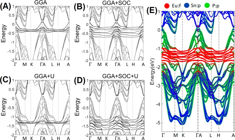
The results of first-principles electronic structure calculations for EuSn2P2 using the generalized gradient approximation (GGA), GGA plus correlation parameter U (GGA+U), and GGA+U with spin–orbit coupling (SOC) are compared in Figure 6. The calculations reveal a semimetallic band structure for this material, with a continuous gap throughout the Brillouin zone, similar in character to what is observed for WTe2.42,43 The electrons in the 4f orbitals of the Eu atoms are experimentally observed (see below) as localized in the range 1.0–2.0 eV below the Fermi level (EF), and thus the GGA+U+SOC calculations appear to be the most representative of the material.
Figure 6.
Calculated electronic structure of bulk EuSn2P2. (A–D) First-principles electronic band structures for EuSn2P2 in its A-type antiferromagnetic ordered state (both spin up and spin down bands are shown) with and without spin–orbit coupling (SOC) and correlation parameter U included. (E) Deconvolution of the electronic structure to show the energy regimes of dominance of the Eu, P, and Sn orbitals.
The calculations show that P 3p orbitals dominate the energy bands just below EF, while Sn 5p orbitals are found below −5 eV and just above EF (Figure 6E). Like is the case for strong topological insulators, Figure 6E shows that in the vicinity of the Fermi energy there are metal states mixed in in significant proportion at the top of the valence band and P states mixed in in significant proportion at the bottom of the conducting band; i.e., there is an inversion of the conventional type of band structure, where this kind of mixing of states above and below EF is negligible. When the effects of spin polarization are included, the total energies of the ferromagnetic (FM) and antiferromagnetic (AFM) models are the lowest (the calculated energy difference between the AFM and FM states in EuSn2P2 is about 13 meV per f.u.), and indicate that the observed antiferromagnetism is energy favored. The magnetic moments, calculated to be about ∼6.7 μB, are solely on the Eu atoms, consistent with what is expected in a naïve picture for this material, where Eu is the only magnetic atom. The electronic structure of the material, calculated for the antiferromagnetically ordered system, shows that the bands near the Fermi level are hybridized among electrons from the p orbitals on the Sn and P atoms. The GGA and GGA+U calculations result in a semimetallic ground state, with no band gap, with Fermi surfaces around the Γ and A points in the Brillouin zone (BZ) (Figure 6A,C).23 When SOC is included in the calculations, a very small (a few meV) band gap is present (Figure 6B,D).
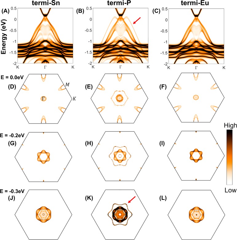
As was designed, EuSn2P2 exhibits interesting surface states. To understand the surface states of EuSn2P2, surface spectral weight simulations consistent with the practice used in the topological materials field were employed. (The first BZ of the rhombohedral lattice is shown in Figure S2.) The (001) surface is our material’s clear cleavage plane. The (001) surface may be terminated by Eu, P, or Sn atomic layers; surface states are visible for all three possible (001) terminations in the calculations. Consistent with the full bulk DFT calculations, the electronic behavior near EF in these calculations is predominantly determined by the dispersion of hybridized bands from Sn and P orbitals. For Sn-terminated and Eu-terminated surfaces, comparison of the bulk and surface calculations (Figure 7) shows that surface states are located in the bulk energy gap around the Γ point. The energy dispersion of these states is very similar to the Dirac surface states of strong Tis (inset of Figure 7D–F). The surface states are more well-separated in k for the P-termination case (Figure 7E) than they are for the Sn- and Eu-termination cases. This should make them more observable experimentally than for the case of WTe2, where they are strongly confined in both energy and wavevector.
Figure 7.
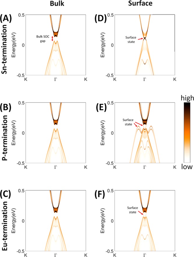
Comparison of the calculated bulk and surface band structures for EuSn2P2. (A–F) Bulk (left) and surface (right) band spectra of a semi-infinite slab with an (001) surface terminated at Sn (upper), P (middle), or Eu (lower) layers. The surface states are the narrow extra states observed in the surface state calculations (right).
It is well-established in materials physics that time-reversal-based topological insulators can be described by a “Z2 invariant”. Generally, Z2 is undefined in a time-reversal symmetry (TRS) breaking system such as a ferromagnetic phase. Nonetheless, recent studies have proposed that the Z2 invariant can be expanded to classify topological states in magnetic systems if the system possesses a specific magnetic configuration, for instance, an antiferromagnetic state, in which the combined symmetry S = ΘT1/2 is preserved, where Θ is the time-reversal operator, and T1/2 is the lattice translational symmetry of the crystal that is broken by the antiferromagnetic order.44,45 This is what we have in the current case. Under this definition, we calculate the Z2 invariant by the Wilson loop method, as shown in Figure 8.46 The Z2 topological invariant can be determined by looking at the evolution of the Wannier function center. In this formalism, the evolution of each Wannier center pair encloses the representation cylinder an integer number of times, which can be viewed as the “winding number” of the Wannier center pair. The Z2 topological number is related to the summation of the winding numbers for all the pairs. If it is odd, then the Z2 topological number is odd. According to Figure 8, the entanglement entropy never becomes zero in the course of any gap- and symmetry-preserving transformation; this demonstrates the nontriviality of the electronic structure of EuSn2P2, i.e., its topological character.
Figure 8.
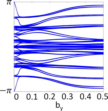
Topological invariant Z2 of EuSn2P2 (calculated with SOC + U). The Wannier charge center evolution (see ref (46)) is shown for time-reversal invariant planes between π and −π. The Wannier center crosses any reference line (hypothetical horizontal line in the figure) the appropriate number of times to indicate that EuSn2P2 is a topological insulator.
Our calculation shows an open curve traversing the entire Brillouin zone in the time-reversal invariant plane kz = 0, indicating a Z2 invariant equal to 1, which demonstrates that EuSn2P2 is indeed an antiferromagnetic topological insulator (AFM-TI).46 The surface state Fermi contours, calculated by way of the semi-infinite Green’s function,47 are shown in Figure 9. The calculated iso-energy band contours at E = 0, −0.2, and −0.3 eV (below the calculated Fermi energy) are shown for the three possible (001) surface terminations. (The energies correspond to those of the surface states on the Sn-terminated surface.48) There is a prominent feature that is seen for the surface band contour in addition to the bulk states directly around the Γ point in the BZ: a 6-fold symmetry loop. The loop is small on the Sn-terminated and Eu-terminated surfaces but is distinctly seen separated from the bulk states in k on the P-terminated surfaces.
Figure 9.
Calculated surface Fermi surfaces of EuSn2P2. For the (001) surface (the cleavage plane), terminated by (A–C) an Eu layer, (D–F) a P layer, or (G, H) a Sn layer. The calculated iso-energy band contours are shown for E = 0 (the calculated Fermi Energy), −0.2, and −0.3 eV for Green’s function surface spectral weight simulation. The depth of the color indicates the weight of the charge density of each state at the surface layer. The surface states clearly appear as the extra ringlike Fermi surfaces in the panels.
Experimentally Observed Surface Electronic Structures
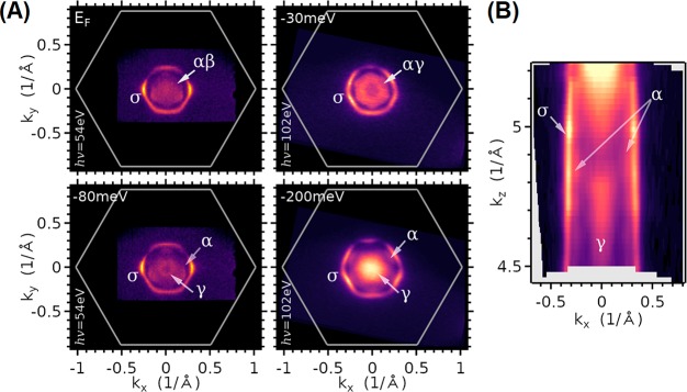
The ARPES spectra, recorded in EuSn2P2’s antiferromagnetically ordered state at 10 K, shown in Figures 10 and 11, reveal the energies of the occupied electronic bands around the center Γ of the (001) surface projection of the bulk BZ. The outer (meaning the band with k vector furthest from the center of the surface BZ) band, designated as σ, disperses linearly at about −0.5 × 10⁶ m/s away from the Fermi level (EF) and appears as a sharp, intense spectral feature at all incident photon energies. This is in contrast with all of the other observed electronic bands and reflects the fact that this is a surface state. Due to the nonconservation of perpendicular-to-plane momenta of the ARPES method, a range of perpendicular momenta is observed in the ARPES spectra of the bulk bands, making them appear as filled-in regions in ARPES maps, distinct from the surface band where the absence of perpendicular dispersion results in a sharp feature. The most notable bulk band is the heart-shaped band, labeled as γ, in the center of the surface BZ, which disperses upward in energy starting from Gamma to about 80 meV below EF and turning again down. The broad bright feature showing little dispersion in the range of energies between −1 and −2 eV (below EF) is from the localized Eu f states.
Figure 10.
Angle-resolved photoemission study of the band structure of EuSn2P2. (A, B) Band dispersion spectra along K−Γ–K taken with 76 and 96 eV photons differ mostly in the relative intensities of the bands due to photoemission selection-rule effects. (C) Incident photon energy 102 eV, shows a wide energy-range band dispersion spectrum along M−Γ–M.
Figure 11.
ARPES study continued. (A) Two-dimensional momentum maps at several energies near the Fermi level obtained with two photon energies to enhance the visibility of different features in the band structure. The surface band, designated as σ, is clearly observed. (B) Photon energy-dependent map to follow the band dispersion along the c crystal axis. The plot is at the energy of −200 meV from EF. (Vo for the kz calculation was set to −10 eV). Different bands are marked with different Greek letters.
As is often the case with surface states, the surface band σ is found relatively close in k-space to one of the bulk bands, labeled as α. Additional bulk bands below EF, labeled as β and δ, are also observed. The constant energy maps, Figure 11, taken at two different incident photon energies (hence, at different kz momenta), show the two-dimensional momentum space surface Fermi surfaces: the hexagonal-loop contour of the surface band σ encloses the contours formed by the bulk bands α, β, and γ. These features greatly resemble the −300 meV band contours calculated for the P termination of EuSn2P2, Figure 9B,E,H, although there is less warping toward the corners of the BZ for the surface band than is calculated.
Momentum space mapping that included a few neighboring surface BZs revealed no bands in the vicinity of the Fermi level other than those shown around Γ in Figure 11. While three other crystal terminations (Eu, Sn single and double layer) cannot be excluded in this material without further theoretical and experimental studies, all our data indicate that the (001) crystal surfaces are indeed P-terminated: the calculations for the Eu and Sn terminations show surface states much closer to the center of the BZ. Moreover, our core level spectra (Figure 12) show that the P 2s levels occur at two energies, indicative of two starkly different chemical environments (thus bulk vs surface) for the P atoms. By comparing the band dispersion observed in the ARPES spectra and the DFT calculations, we conclude that the cleaved crystals are some 220 meV hole doped. This is consistent with the large p-type carrier concentration observed in the Hall measurements.
Figure 12.
Chemistry of the surface core level spectrum of EuSn2P2 measured using 300 eV incident photons. This shows that the P has two different environments (there is only one type of P in the bulk crystal structure) and therefore is present in both the bulk and the surface.
We note that the calculations show the bottom of six elliptical electron pockets around the M point of the BZ, which are slightly above the chemical potential (about −220 meV compared to the calculated EF) observed in the ARPES experiments. This explains why no trace of those calculated bands is seen in ARPES (which sees only filled states) and further gives a hint for why the results of potassium adsorption measurements, expected to electron-dope the surface, resulted in no noticeable band shifts—the flat bottom of an electron pocket is associated with a high density of states, and all the states have to be filled for the shifts in other bands to be observed. We also note that our ARPES measurements at varying incident photon energies show remarkably little difference in the band structure of EuSn2P2 at different perpendicular momenta kz. The bands, most notably the surface state σ, Figures 10 and 11, show little dispersion perpendicular to the layers. The three-dimensional Fermi surface thus consists of hexagonally warped cylinders formed by extruding the contours of the bulk bands α and β along the crystal axis c (Figure 11B).
Summary and Conclusions
The novel quantum material EuSn2P2 was designed based on chemical criteria to display both magnetism and electronic surface states. The hypothesized material was discovered, and crystals were grown using the Sn-flux method. Its crystal structure and physical properties were characterized. Its crystal structure consists of hexagonal Eu, and P layers surrounding a Sn bilayer. It has a positive Curie–Weiss temperature of ΘCW = 31(1) K, showing the dominance of ferromagnetic spin correlations at high temperatures, but it orders antiferromagnetically near 30 K. Its ordered magnetic structure, refined from neutron diffraction, shows antiferromagnetically coupled in-plane-ferromagnetic Eu2+ layers. The temperature-dependent resistance of EuSn2P2 is weakly metallic in character, and an anomalous magnetoresistance is found below the magnetic ordering temperature and below applied magnetic fields of 4 T, where the magnetization saturates with applied magnetic field.
Electronic structure calculations support magnetic ordering as the energetically stable state of the system at low temperatures, and further confirm that the observed magnetic moments solely arise from the Eu2+ present. Calculations including both SOC and correlation parameter U best describe the positions of the Eu f states between 1 and 2 eV below EF, and further show that EuSn2P2 is an antiferromagnetic topological insulator (the energies of the valence band and conduction bands overlap but for electrons of different wave vectors in the Brillouin zone). The bulk band structure is unconventional in that metal states contribute significantly just below the Fermi energy while nonmetal states contribute significantly just above the Fermi energy. The calculations also predict the presence of Dirac-like surface states within the bulk energy gap, both above and below the Fermi energy. The experimental ARPES study shows that surface states are indeed present in the antiferromagnetically ordered state at 10 K but differ in a minor way from the calculations for a P-terminated (001) surface. Although we have observed much about the basic properties of this new quantum material, more detailed work on the properties from the physics perspective is required to determine whether it is unique in that it shows both antiferromagnetism and surface states at low temperatures. The accessible temperatures involved, the simple crystal structure, the ability to fabricate bulk crystals, and the combination of properties make the quantum material EuSn2P2 an ideal platform for the detailed study of the interplay of topological electronic states with magnetism.
Acknowledgments
The work at Princeton was supported by the ARO MURI on Topological Insulators, Grant W911NF1210461. W.X. at LSU was supported by a Beckman Young Investigator award. X.G. at LSU is supported by the National Science Foundation under NSF-OIA-1832967. H.B.C. acknowledges support of US DOE BES Early Career Award KC0402010 under Contract DE-AC05-00OR22725. This research used resources at the High Flux Isotope Reactor, a DOE Office of Science User Facility operated by the Oak Ridge National Laboratory. This research also used resources of the National Synchrotron Light Source II, a U.S. Department of Energy (DOE) Office of Science User Facility operated for the DOE Office of Science by Brookhaven National Laboratory under Contract DE-SC0012704. I.P. thanks J. Jiang, E. Vescovo, and K. Kaznatcheev for their help with setting up the experiment at the 21-ID-1 (ESM-ARPES) beamline. T.-R.C. was supported from Young Scholar Fellowship Program by Ministry of Science and Technology (MOST) in Taiwan, under MOST Grant for the Columbus Program MOST108-2636-M-006-002 and MOST 107-2627-E-006-001. W.X. and X.G. thank D. Vineyard for helping with electron paramagnetic resonance measurement.
Supporting Information Available
The Supporting Information is available free of charge on the ACS Publications website at DOI: 10.1021/acscentsci.9b00202.
Field-dependence of ρxx for various temperatures for sample 2; magnetoresistance at the same temperatures for sample 2; first Brillouin zone of the rhombohedral lattice with the high symmetry momentum points marked (Γ–M–K) (PDF)
The authors declare no competing financial interest.
Supplementary Material
References
- Awschalom D. D.; Bassett L. C.; Dzurak A. S.; Hu E. L.; Petta J. R. Quantum Spintronics: Engineering and Manipulating Atom-Like Spins in Semiconductors. Science 2013, 339, 1174–1179. 10.1126/science.1231364. [DOI] [PubMed] [Google Scholar]
- Cirac J. I.; Zoller P. Goals and Opportunities in Quantum Simulation. Nat. Phys. 2012, 8, 264–266. 10.1038/nphys2275. [DOI] [Google Scholar]
- Ladd T. D.; Jelezko F.; Laflamme R.; Nakamura Y.; Monroe C.; O’Brien J. L. Quantum Computers. Nature 2010, 464, 45–53. 10.1038/nature08812. [DOI] [PubMed] [Google Scholar]
- Moore J. E. The Birth of Topological Insulators. Nature 2010, 464, 194–198. 10.1038/nature08916. [DOI] [PubMed] [Google Scholar]
- Sato M.; Ando Y. Topological Superconductors: A Review. Rep. Prog. Phys. 2017, 80 (7), 076501. 10.1088/1361-6633/aa6ac7. [DOI] [PubMed] [Google Scholar]
- Li R.; Wang J.; Qi X.-L.; Zhang S.-C. Dynamical Axion Field in Topological Magnetic Insulators. Nat. Phys. 2010, 6, 284–288. 10.1038/nphys1534. [DOI] [Google Scholar]
- Chang C.-Z.; Zhao W.; Kim D. Y.; Zhang H.; Assaf B. A.; Heiman D.; Zhang S.-C.; Liu C.; Chan M. H. W.; Moodera J. S. High-Precision Realization of Robust Quantum Anomalous Hall State in a Hard Ferromagnetic Topological Insulator. Nat. Mater. 2015, 14, 473–477. 10.1038/nmat4204. [DOI] [PubMed] [Google Scholar]
- Chang C.-Z.; Zhang J.; Feng X.; Shen J.; Zhang Z.; Guo M.; Li K.; Ou Y.; Wei P.; Wang L.-L.; et al. Experimental Observation of the Quantum Anomalous Hall Effect in a Magnetic Topological Insulator. Science 2013, 340, 167–170. 10.1126/science.1234414. [DOI] [PubMed] [Google Scholar]
- Katmis F.; Lauter V.; Nogueira F. S.; Assaf B. A.; Jamer M. E.; Wei P.; Satpati B.; Freeland J. W.; Eremin I.; Heiman D.; et al. A High-Temperature Ferromagnetic Topological Insulating Phase by Proximity Coupling. Nature 2016, 533, 513–516. 10.1038/nature17635. [DOI] [PubMed] [Google Scholar]
- Mogi M.; Kawamura M.; Yoshimi R.; Tsukazaki A.; Kozuka Y.; Shirakawa N.; Takahashi K. S.; Kawasaki M.; Tokura Y. A Magnetic Heterostructure of Topological Insulators as a Candidate for an Axion Insulator. Nat. Mater. 2017, 16, 516–521. 10.1038/nmat4855. [DOI] [PubMed] [Google Scholar]
- Slager R.-J.; Mesaros A.; Juričić V.; Zaanen J. The Space Group Classification of Topological Band-Insulators. Nat. Phys. 2013, 9, 98–102. 10.1038/nphys2513. [DOI] [Google Scholar]
- Yang K.; Setyawan W.; Wang S.; Buongiorno Nardelli M.; Curtarolo S. A Search Model for Topological Insulators with High-Throughput Robustness Descriptors. Nat. Mater. 2012, 11, 614–619. 10.1038/nmat3332. [DOI] [PubMed] [Google Scholar]
- Vergniory M. G.; Elcoro L.; Felser C.; Bernevig B. A.; Wang Z.. The (High Quality) Topological Materials In The World. 2018, arXiv:1807.10271. arXiv e-Print archive. https://arxiv.org/abs/1807.10271.
- Po H. C.; Vishwanath A.; Watanabe H. Symmetry-Based Indicators of Band Topology in the 230 Space Groups. Nat. Commun. 2017, 8 (1), 50. 10.1038/s41467-017-00133-2. [DOI] [PMC free article] [PubMed] [Google Scholar]
- Tang F.; Po H. C.; Vishwanath A.; Wan X. Towards Ideal Topological Materials: Comprehensive Database Searches Using Symmetry Indicators. Nature 2019, 566, 486. 10.1038/s41586-019-0937-5. [DOI] [PubMed] [Google Scholar]
- Bradlyn B.; Elcoro L.; Cano J.; Vergniory M. G.; Wang Z.; Felser C.; Aroyo M. I.; Bernevig B. A. Topological Quantum Chemistry. Nature 2017, 547, 298–305. 10.1038/nature23268. [DOI] [PubMed] [Google Scholar]
- Nesper R. The Zintl-Klemm Concept – A Historical Survey. Z. Anorg. Allg. Chem. 2014, 640 (14), 2639–2648. 10.1002/zaac.201400403. [DOI] [Google Scholar]
- Gui X.; Sobczak Z.; Chang T.-R.; Xu X.; Huang A.; Jia S.; Jeng H.-T.; Klimczuk T.; Xie W. Superconducting SrSnP with Strong Sn–P Antibonding Interaction: Is the Sn Atom Single or Mixed Valent?. Chem. Mater. 2018, 30, 6005–6013. 10.1021/acs.chemmater.8b02258. [DOI] [Google Scholar]
- Hsieh T. H.; Lin H.; Liu J.; Duan W.; Bansil A.; Fu L. Topological Crystalline Insulators in the SnTe Material Class. Nat. Commun. 2012, 3, 982. 10.1038/ncomms1969. [DOI] [PubMed] [Google Scholar]
- Deng J.; Xia B.; Ma X.; Chen H.; Shan H.; Zhai X.; Li B.; Zhao A.; Xu Y.; Duan W.; et al. Epitaxial Growth of Ultraflat Stanene with Topological Band Inversion. Nat. Mater. 2018, 17, 1081. 10.1038/s41563-018-0203-5. [DOI] [PubMed] [Google Scholar]
- Checkelsky J. G.; Hor Y. S.; Cava R. J.; Ong N. P. Bulk Band Gap and Surface State Conduction Observed in Voltage-Tuned Crystals of the Topological Insulator Bi2Se3. Phys. Rev. Lett. 2011, 106, 196801. 10.1103/PhysRevLett.106.196801. [DOI] [PubMed] [Google Scholar]
- Zhang H.; Liu C.-X.; Qi X.-L.; Dai X.; Fang Z.; Zhang S.-C. Topological Insulators in Bi2Se3Bi2Te3 and Sb2Te3 with a Single Dirac Cone on the Surface. Nat. Phys. 2009, 5, 438–442. 10.1038/nphys1270. [DOI] [Google Scholar]
- Chang T.-R.; Pletikosic I.; Kong T.; Bian G.; Huang A.; Denlinger J.; Kushwaha S. K.; Sinkovic B.; Jeng H.-T.; Valla T.; et al. Realization of a Type-II Nodal-Line Semimetal in Mg3Bi2. Adv. Sci. 2019, 6, 1800897. 10.1002/advs.201800897. [DOI] [PMC free article] [PubMed] [Google Scholar]
- Borisenko S.; Evtushinsky D.; Gibson Q.; Yaresko A.; Kim T.; Ali M. N.; Buechner B.; Hoesch M.; Cava R. J.. 2015, Time-Reversal Symmetry Breaking Type-II Weyl State in YbMnBi2. arXiv:1507.04847. arXiv e-Print archive. https://arxiv.org/abs/1507.04847. [DOI] [PMC free article] [PubMed]
- Rong L.-Y.; Ma J.-Z.; Nie S.-M.; Lin Z.-P.; Li Z.-L.; Fu B.-B.; Kong L.-Y.; Zhang X.-Z.; Huang Y.-B.; Weng H.-M.; et al. Electronic Structure of SrSn2As2 near the Topological Critical Point. Sci. Rep. 2017, 7 (1), 6133. 10.1038/s41598-017-05386-x. [DOI] [PMC free article] [PubMed] [Google Scholar]
- Heremans J. P.; Cava R. J.; Samarth N. Tetradymites as Thermoelectrics and Topological Insulators. Nat. Rev. Mater. 2017, 2 (10), 17049. 10.1038/natrevmats.2017.49. [DOI] [Google Scholar]
- Cava R. J.; Ji H.; Fuccillo M. K.; Gibson Q. D.; Hor Y. S. Crystal Structure and Chemistry of Topological Insulators. J. Mater. Chem. C 2013, 1, 3176–3189. 10.1039/c3tc30186a. [DOI] [Google Scholar]
- Goto Y.; Yamada A.; Matsuda T. D.; Aoki Y.; Mizuguchi Y. SnAs-Based Layered Superconductor NaSn2As2. J. Phys. Soc. Jpn. 2017, 86, 123701. 10.7566/JPSJ.86.123701. [DOI] [Google Scholar]
- Sheldrick G. M. Crystal Structure Refinement with SHELXL. Acta Crystallogr., Sect. C: Struct. Chem. 2015, 71 (1), 3–8. 10.1107/S2053229614024218. [DOI] [PMC free article] [PubMed] [Google Scholar]
- Sheldrick G. M. A Short History of SHELX. Acta Crystallogr., Sect. A: Found. Crystallogr. 2008, 64, 112–122. 10.1107/S0108767307043930. [DOI] [PubMed] [Google Scholar]
- Spek A. L. Single-Crystal Structure Validation with the Program PLATON. J. Appl. Crystallogr. 2003, 36, 7–13. 10.1107/S0021889802022112. [DOI] [Google Scholar]
- Spek A. L. PLATON SQUEEZE: A Tool for the Calculation of the Disordered Solvent Contribution to the Calculated Structure Factors. Acta Crystallogr., Sect. C: Struct. Chem. 2015, 71, 9–18. 10.1107/S2053229614024929. [DOI] [PubMed] [Google Scholar]
- Rodríguez-Carvajal J. Recent Advances in Magnetic Structure Determination by Neutron Powder Diffraction. Phys. B 1993, 192, 55–69. 10.1016/0921-4526(93)90108-I. [DOI] [Google Scholar]
- Hafner J. Ab-Initio Simulations of Materials Using VASP: Density-Functional Theory and Beyond. J. Comput. Chem. 2008, 29, 2044–2078. 10.1002/jcc.21057. [DOI] [PubMed] [Google Scholar]
- Perdew J. P.; Burke K.; Ernzerhof M. Generalized Gradient Approximation Made Simple. Phys. Rev. Lett. 1996, 77, 3865–3868. 10.1103/PhysRevLett.77.3865. [DOI] [PubMed] [Google Scholar]
- Dahl J. P.; Avery J.. Local Density Approximations in Quantum Chemistry and Solid State Physics; Springer Science & Business Media, 2013. [Google Scholar]
- Anisimov V. I.; Aryasetiawan F.; Lichtenstein A. I. First-Principles Calculations of the Electronic Structure and Spectra of Strongly Correlated Systems: The LDA+U method. J. Phys.: Condens. Matter 1997, 9, 767–808. 10.1088/0953-8984/9/4/002. [DOI] [Google Scholar]
- Shim J. H.; Haule K.; Kotliar G. Modeling the Localized-to-Itinerant Electronic Transition in the Heavy Fermion System CeIrIn5. Science 2007, 318, 1615–1617. 10.1126/science.1149064. [DOI] [PubMed] [Google Scholar]
- Monkhorst H. J.; Pack J. D. Special Points for Brillouin-Zone Integrations. Phys. Rev. B 1976, 13, 5188–5192. 10.1103/PhysRevB.13.5188. [DOI] [Google Scholar]
- Kittel C.Introduction to Solid State Physics Global ed.; Wiley: Hoboken, NJ, 2018. [Google Scholar]
- Ashcroft N. W.; Mermin N. D.. Solid State Physics; Saunders College, 1976. [Google Scholar]
- Pletikosić I.; Ali M. N.; Fedorov A. V.; Cava R. J.; Valla T. Electronic Structure Basis for the Extraordinary Magnetoresistance in WTe2. Phys. Rev. Lett. 2014, 113 (21), 216601. 10.1103/PhysRevLett.113.216601. [DOI] [PubMed] [Google Scholar]
- Ali M. N.; Xiong J.; Flynn S.; Tao J.; Gibson Q. D.; Schoop L. M.; Liang T.; Haldolaarachchige N.; Hirschberger M.; Ong N. P.; et al. Large, Non-Saturating Magnetoresistance in WTe2. Nature 2014, 514, 205–208. 10.1038/nature13763. [DOI] [PubMed] [Google Scholar]
- Mong R. S.; Essin A. M.; Moore J. E. Antiferromagnetic Topological Insulators. Phys. Rev. B: Condens. Matter Mater. Phys. 2010, 81, 245209. 10.1103/PhysRevB.81.245209. [DOI] [Google Scholar]
- Fang C.; Gilbert M. J.; Bernevig B. A. Topological Insulators with Commensurate Antiferromagnetism. Phys. Rev. B: Condens. Matter Mater. Phys. 2013, 88, 085406. 10.1103/PhysRevB.88.085406. [DOI] [Google Scholar]
- Yu R.; Qi X. L.; Bernevig A.; Fang Z.; Dai X. Equivalent Expression of Z2 Topological Invariant for Band Insulators Using the Non-Abelian Berry Connection. Phys. Rev. B: Condens. Matter Mater. Phys. 2011, 84, 075119. 10.1103/PhysRevB.84.075119. [DOI] [Google Scholar]
- Skriver H. L.; Rosengaard N. M. Self-Consistent Green’s-Function Technique for Surfaces and Interfaces. Phys. Rev. B: Condens. Matter Mater. Phys. 1991, 43, 9538–9549. 10.1103/PhysRevB.43.9538. [DOI] [PubMed] [Google Scholar]
- King P. D. C.; Hatch R. C.; Bianchi M.; Ovsyannikov R.; Lupulescu C.; Landolt G.; Slomski B.; Dil J. H.; Guan D.; Mi J. L.; et al. Large Tunable Rashba Spin Splitting of a Two-Dimensional Electron Gas in Bi2Se3. Phys. Rev. Lett. 2011, 107 (9), 096802. 10.1103/PhysRevLett.107.096802. [DOI] [PubMed] [Google Scholar]
Associated Data
This section collects any data citations, data availability statements, or supplementary materials included in this article.


