Abstract
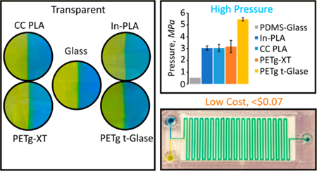
Transparent surfaces within microfluidic devices are essential for accurate quantification of chemical, biological, and mechanical interactions. Here, we report how to create low-cost, rapid 3D-printed microfluidic devices that are optically free from artifacts and have transparent surfaces suitable for visualizing a variety of fluid phenomenon. The methodology described here can be used for creating high-pressure microfluidic systems (significantly higher than PDMS–glass bonding). We develop methods for annealing Poly-Lactic Acid (PLA) microfluidic devices demonstrating heat resistance typically not achievable with other plastic materials. We show DNA melting and subsequent fluorescent imaging analysis, opening the door to other high-temperature applications. The FDM techniques demonstrated here allow for fabrication of microfluidic devices for precise visualization of interfacial dynamics, whether mixing between two laminar streams or droplet tracking. In addition to these characterizations, we include a printer troubleshooting guide and printing recipes for device fabrication to facilitate FDM printing for microfluidic device development.
Graphical Abstract
Microfluidics is the study of fluid movement and interaction at the micrometer scale. At this scale, controlled fluid manipulation leads to unique applications that are not feasible in macroscale regimes such as inertial flow focusing,1 digital droplet manipulation,2 microfluidic self-assembly,3 cell manipulation,4 centrifugal microfluidics,5 and others. Complex fluid manipulation is not necessarily characterized by complex fabrication protocols. For example, straightforward microfluidic device fabrication methods include soft lithography,6 xurography,7 and paper-based microfluidics.8 The predominant barriers for new uses and users are device fabrication expertise and access to expensive equipment. 3D printing promises to be an enabling technology that reduces complexity and cost and thus expands the realm of micro and nanofluidics.
A variety of 3D printing techniques are available, including multijet modeling (MJM), fused deposition modeling (FDM), stereolithography (SLA), and two-photon polymerization (2PP).9 FDM utilizes a heated nozzle and the extrusion of a plastic filament in 2D layers to form the desired three-dimensional object.10 This approach presents a number of advantages over other 3D printing methods, including relatively inexpensive materials and printers, a large selection of materials, the ease of initial use, and the ability to start, stop, and integrate complexity on the fly.9,11 Standing criticisms of FDM printing include poor planar printing control where variations exist between actual and designed prints12,13 and poor layer adhesion leading to interlayer fluid leaking and poor pressure profiles. FDM accuracy depends on the alignment of the x, y, and z components, because belt tension, motor microstepping, threaded rod pitch, and other factors directly impact resolution at the micrometer scale. Material printing properties influence deposition rate, spreading, adhesion, and cooling, further influencing resolution and device performance. Clear instructions and guidelines for printing microfluidic devices as a function of material are typically not included, and if they are, they do not contain sufficient information to efficiently reproduce the original design.
Dimensional accuracy coupled with transparency on a 3D printed platform is highly desirable but difficult to achieve. Transparent microfluidic devices printed using SLA14 and PolyJet15 family of printers has been demonstrated. These approaches create completely transparent, clean structures, whereas the focus here is on creating a transparent surface that rivals the quality of the aforementioned techniques. While SLA techniques can produce transparent devices, the need for postprint cleaning and lack of complete fabrication control limit their applications. For instance, using an FDM printer, a membrane or an electrode can be directly integrated into a microfluidic device by simply pausing the print. The PolyJet family of printers have similar limitations to SLA with the addition of being expensive ($20,000 to >$200,000). Optically clear microfluidic devices enable on-chip classification and quantification of chemical and biological reactions. Transparency is also important for studying fluid behavior generally, because it allows for rapid quantification of lamina mixing16 and reaction kinetics.17 While transparent microfluidic devices have been demonstrated, most images of fluid flow are taken at low magnification, reducing the impact of 3D printing artifacts.18–20 Printed surfaces rivaling the clarity of glass have yet to be demonstrated with FDM printers but are critical for a number of applications including droplet tracking. Droplets fabricated within 3D printed microfluidic devices are typically characterized by hand.18,21–23 For applications where thousands of droplets are analyzed based on size, intensity, and curvature, manual characterization is not feasible. Automated droplet tracking solves this problem but requires artifact-free surfaces for accurate characterization, which has yet to be satisfactorily demonstrated.
Channel dimensions using commercially available and general-purpose 3D printers below $3000 typically exceed 500 μm in height or/and width,18,24 so they are of limited value in microfluidics. Now an off-the-shelf printer (e.g., Fluidic Factory (FF) by Dolomite Microfluidics, ∼$25,000), designed specifically for fabricating leak-free and transparent microfluidic devices using cyclic olefin copolymer (COC), can be purchased, with channel dimensions of around 300 μm.25 This product is speeding the transition of microfluidic systems to commercial applications, but cost and material restrictions seriously limit the utility of this approach. While the methodology for creating sealed microfluidic devices described here is similar to that employed by FF, we are able to create devices of superior transparency, at a much lower printer cost with access to a much larger selection of materials.
To address the need for low-cost, high-quality microfluidic devices, in this work, we present print recipes for creating devices with glass-like transparent surfaces using off-the-shelf FDM printers. We perform all characterization at high magnification, where air entrapment, layer deviation, material impurities, and poor printing protocols will directly impact the quality of printed devices and subsequent observation.26 To accomplish this work, we develop methodology for creating highly transparent, glass-like 3D printed surfaces for visualizing fluid interactions. We integrate this process into a general printing protocol to create complex structures from a single print without the need for post processing or supporting structures. We demonstrate consistent formation of 400 × 400 μm square channels, the smallest enclosed channels manufactured to date utilizing affordable, commercially available FDM printers. We compare two models (Prusa i3 (US $600) and LulzBot (US $2500)) and show that precise and reproducible printing is a function of the chosen materials and printer settings, rather than the printer itself. Both can be used to manufacture research-grade microfluidic devices capable of droplet generation and interface tracking. We show that transparent and leak-free devices are mainly a function of the printing parameters and are readily obtained using protocols presented here. We also show that 3D printed devices can have burst pressures at least 5 times higher than those typical of soft lithography devices.
Further, we demonstrate a significant increase in heat resistance after annealing of PLA, opening up applications in high-temperature environments such as DNA melting analysis. We also noted that noise from autofluorescence was significantly reduced within annealed PLA devices, resulting in improved signal-to-noise ratio and quantitation. As proof-of-concept, we perform DNA melting and quantification analysis using annealed PLA microfluidic devices. To facilitate rapid adoption by the community, we provide a troubleshooting guide that details common problems and our solutions for making FDM 3D printed microchannels.
EXPERIMENTAL SECTION
Materials.
In-PLA (polylactic acid), t-Glase PETg (polyethylene terephthalate glycol), and Nylon-680 were purchased from Taulman3D. PLA Crystal Clear was purchased from Fillamentum. PETg XT was purchased from ColorFabb. New, clean glass slides were obtained from Fisher Scientific (Microscope Slides, 25 × 75 × 1 mm, Fisherfinest). All syringes were purchased from BDPlastics. Mineral oil and dye (Sudan Black) was purchased from Sigma-Aldrich. Tygon 0.02 × 0.06″ tubing was purchased from Cole-Parmer. UV curable adhesive (3106) was purchased from Loctite. Dodecyl sodium sulfate (SDS) was purchased from Mallinckrodt Chemicals. LC Green Plus (LCGreen) dye was obtained from Biofire Defense. LEDs were band gap filtered to 450 ± 25 nm (HQ450/50X, Chroma Technology Corp, VT, USA). A light microscope was fitted with a 485 nm long-pass filter (HQ485LP, Chroma Technology Corp, VT, USA) for fluoresce excitation.
Device Fabrication and Characterization.
All designs were created in Solidworks 2016. Designs were exported as .STL files and imported into Slic3r Prusa Edition (Prusa). Designs were printed on an Original Prusa i3MK2S (Prusa) with a 0.4 mm nozzle and Lulzbot TAZ6 with a 0.5 mm nozzle. Most chips were printed using Prusa i3, except for devices used for printer characterization. Original Prusa i3MK2S was used to print with PETg-XT and CC-PLA. Lulzbot TAZ6 was used to print with PETg t-Glase and In-PLA with results presented in Figure 1a. Each material required unique printing parameters with a summary found in Supplementary Figure S1. Configuration files (.INI) for each material are included (Supporting Information). The first layer was always printed at a distance of 30 μm from the nozzle tip to the glass surface at a starting height of 100 μm. The calibrated z-height for the Prusa i3 is −550 μm. This height is adjusted for printing onto a glass slide by setting a z-offset in the Prusa Sli3er software to 1 mm (height of glass slide). In order to immobilize the glass slide, a rectangular frame, 0.5 mm in height, was printed onto the bed. Next, the glass slide was placed into this frame. Adjusting the bed temperature was not necessary. Next, the calibrated z-height is set to−580 μm (30 μm closer to the glass surface). Upon completion of the first layer, the nozzle was raised from the surface by 30 μm for the remainder of the print. 90° (horizontal and vertical) fill orientations at a layer height of 50 μm were used for all prints. Further, infill/parameter overlap was set to 175% to eliminate gaps between layers. The ability to reproduce channel widths and heights was tested by printing channels ranging in width from 300 μm to 1 mm in both directions (n = 3). The same designs were used across all materials (n = 3). Height, width, and cross-sectional areas were measured using digital microscopy (AM7115MZ 5MP, Dino-Lite). Cross sections were measured by physically slicing printed channels in the middle of the printed structure. ImageJ was utilized for quantifying deformation.
Figure 1.
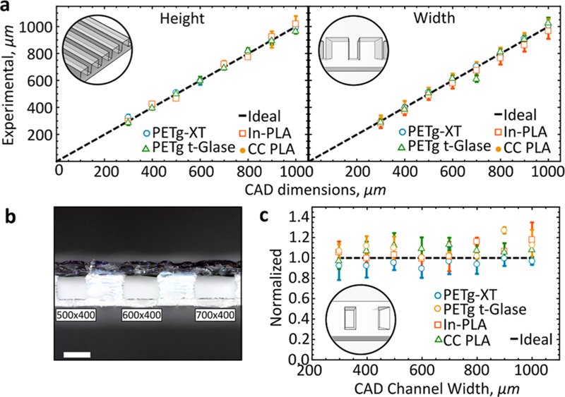
Printer characterization. (a) Measured height and width of printed channels printed with four different filaments. All measured pieces are compared to designed CAD dimensions (n = 9). (b) Cross-sectional cut of a printed test piece (In-PLA) (n = 3). Scale bar, 0.5 mm. (c) Measured cross-sectional area compared to designed (ideal).
Mixing and Transparency Characterization.
Devices were printed onto clean glass slides and released from the surface with filtered, deionized water. After the addition of tubing, two 3 mL syringes were loaded with blue and yellow dye, respectively. One syringe was attached to one inlet port and the other syringe to the other. Tygon inlet tubes were affixed to the inlet and outlet ports via UV curable adhesive (long wavelength, 30 min curing time); other glues with faster curing times can also be used. Dye was pushed through the device using a syringe pump (KD Scientific) at a constant flow rate of 50 μL/min. The dye interface was monitored in real time using a portable light microscope. Transparency in Figure 2d was compared to that of a microfluidic chip fabricated on top of a glass slide (1 mm thickness).
Figure 2.
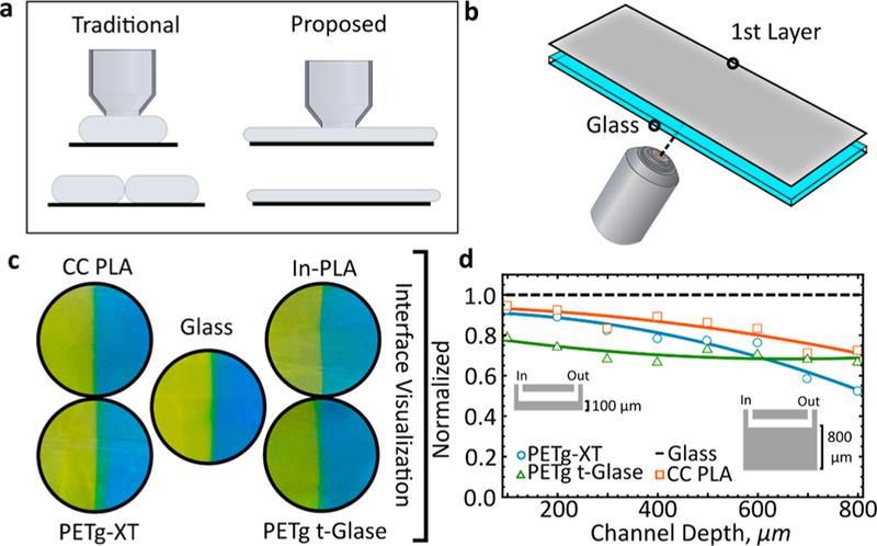
Transparency characterization. (a) Printing methodology for improving microfluidic device clarity. The traditional approach is contrasted to the method proposed in this paper. (b) Schematic demonstrating fabrication of the transparent layer. (c) Interface visualization of two touching laminar streams (yellow and blue dye) within a microfluidic device. (d) A 400 × 400 μm channel is printed onto an ever-thicker visualization layer. Transparency of the blue and yellow surface is quantitatively compared for all four materials to that of glass. Scale bar, 500 μm.
Droplet Formation and Tracking.
Oil-in-water droplets were formed within a PETg-XT microfluidic device. Two 3 mL syringes were attached to the device, one syringe delivering mineral oil saturated with Sudan Black dye (0.002%) (dispersed phase), and the other delivering deionized water with 2% SDS (continuous phase). Water flow rate was held constant at 1 uL/min while the continuous phase flow rate was varied. Droplets were recorded using an optical microscope at 10 fps. Unaltered video was loaded into Droplet Morphometry and Velocimetry (DMV) software provided by Dr. Amar S. Basu. Successful application of automated tracking software requires background image subtraction, edge detection, small object and border removal, shape fill, shape discrimination, and frame correlation.27
DNA Melting Characterization.
Devices were printed in Crystal Clear PLA. Each device takes 45 min to print. Considering the surface area of the printing bed is 250 × 210 mm, 20 devices can be printed overnight and be ready for testing the following day. A thermal gradient is applied by placing the chip onto a steel plate situated on top of two heated copper blocks that are separated by 26 mm. Steel bridge dimensions are 76 mm long, 28 mm wide, and 6 mm thick. Both ends of the microfluidic device are heated to the desired temperatures. Thin heaters are placed beneath the copper blocks allowing for direct thermal control. In this way, a thermal gradient is formed across the steel plate, which bridges the copper blocks, readily defining hot and cold sections across the device. Copper blocks were heated to 83 and 70 °C, respectively. Thermocouples were placed directly on top of the 3D printed chip. The thermocouples had an accuracy of ±0.5 °C and were the main limit of thermal resolution in the experiment. The chip was illuminated with LEDs that are band-pass filtered, with another filter placed in front of the camera so that only the LCGreen fluorescence is collected in the camera. A thermocouple placed in the center of the device (not obstructing the channel), close to the melting point of the DNA, allows for calibration of the linear thermal gradient to the exact location on the chip. For each experiment, 20 μL of sample was loaded into the chip. The melting temperature (Tm) of DNA obtained in this work was compared to that obtained from a commercially available instrument (HR-1, Idaho Technology, Salt Lake City, UT), which requires 10 μL of sample per melt.
RESULTS AND DISCUSSION
Printer Characterization.
We tested our ability to control and replicate channels of varying heights and widths using two different 3D printers. Here, we show that the average channel width variation was 0.32% with a height variation of just 0.08% across all tested print channels (Figure 1). A simple, linearly increasing design was used to test the robustness of the printers in producing these designs. The results of the linearly increasing channel widths and heights are shown in Figure 1. Measured channel dimensions closely matched designed specifications (Figure 1a,b) regardless of the printer. A table summarizing optimal printing conditions is provided (Supplementary Figure S1).
Next, the ability to create closed channels was investigated (Figure 1b). As expected, most channels could be readily closed, without significant cross-sectional distortion. As channel width increased beyond 700 μm, to 1 mm, average error increased from 4 to 10% of the designed cross-sectional width (Figure 1c). As the channel dimensions increase in the x-direction (width), bridging becomes much harder because of material sag and subsequent channel filling. Bridging proved to be universally challenging across all tested materials, with some materials performing slightly better (Figure 1c). Best results are obtained when the print is aligned perpendicularly to the fan. Direct cooling into the channel ensures consistent, ooze-free material deposition and reproducible bridging of the open channels. Since closed channels are created in a single step (no supporting structures), the methodology provided here demonstrates rapid formation of closed channels with no postprocessing work required. We found optimal print conditions for each material, demonstrating that with appropriate settings, the impact of material properties like sag could be minimized. Printing closed channels with PETg t-Glase proved the most challenging, for example, the slow speeds required for layer bonding and transparency resulted in hard to control bridging, leading to channel deformations (>27% for 900 μm wide channels). To facilitate faster translation of CAD designs into 3D printed devices, we provide a troubleshooting guide that covers the most commonly encountered issues during 3D printing (Supplementary Figure S2). Following these optimized printing recipes will lead to closed channels below 400 × 400 μm.
Glass-like Layer (gL2).
We found that transparency is a function of nozzle temperature, print speed, and cooling rate. Rather than fabricating entirely transparent devices, we realized that many applications require a device in which only the bottom surface is completely transparent (Figure 2). Therefore, we generated a glossy and highly transparent first layer by printing directly onto a clean microscope glass slide, preheated on top of the heated print bed. Lowering the nozzle closer to the surface of the glass slide by ∼30 μm resulted in a completely sealed and a highly transparent first layer (Figure 2a,b).
First, we compare four commercially available transparent materials, two PLA and two PETg filaments, and highlight the impact of material composition on transparency across a number of manufacturers. By fabricating a simple T-junction microfluidic mixer, we can clearly resolve the fluid dye interface and compare it to a device made with glass (Figure 2c). The transparent layer shows none of the typical FDM artifacts; thin white lines, air gaps, and pockets are completely eliminated. Next, we printed the T-channel deeper and deeper into the device (Figure 2d). At a layer thickness of 100 μm (1st layer thickness), transparency of the glass-like printed layer is almost identical to glass. Normalization based on thickness is also provided in Figure S6. Transparency steadily decreases for most materials as more layers are printed on top off the first layer. Up to a depth of 600 μm, the dye interface is still easily distinguishable (Supplementary Figure S3). Only PETg t-Glase yielded consistently clear surfaces at depths of 700 μm and greater. As depth increased, transparency reduced because of entrapment of microscopic air bubbles and light scattering from poorly bonded layers. Even with perfect layer alignment, transparency always decreases with depth. When using 3D printed microfluidic devices, channels that require optical examination should be placed near the imaged surface of the channel. The methodology described here also applies to creating threaded structures within microfluidic devices; however, transparency constraints must be kept in mind (Supplementary Figure S4). A hazy surface with increasing channel depth was the norm for all tested materials, with the noted exception of PETg t-Glase. Unfortunately, because of continuous delamination from the glass surface, it was not possible to print In-PLA devices for transparency characterization.
Next, we tested material resistance to deformation. A serpentine microfluidic device with 41 turns and a single inlet was used as a benchmark. By creating a tight network of channels, we are able to directly test for both internal (between channel) and external leaks. The 100 μm, glass-like transparent layer, on average, resisted pressures of up 3 MPa (Supplementary Figure S5). The material composition of PETg t-Glase resulted in device failure at pressures almost double that required for the rest of the tested materials (5.5 ± 0.2 MPa). No cross channel, cross layer, or general device leaking was observed until critical failure.
Tracking Small Intensity Changes.
We printed a serpentine microfluidic mixer to demonstrate controlled printing of the glass-like layer (gL2) over the surface of a glass slide covering an area of 65 × 20 mm. A simple T-junction was used to bring the fluids into contact, followed by diffusive mixing along the length of the device (Figure 3b). While 400 × 400 μm channels are easily reproducible, we note that sharp, 90° angles are impossible to obtain with our configuration, because the circular nature of the extruding nozzle leads to rounded profiles (Figure 3a).
Figure 3.
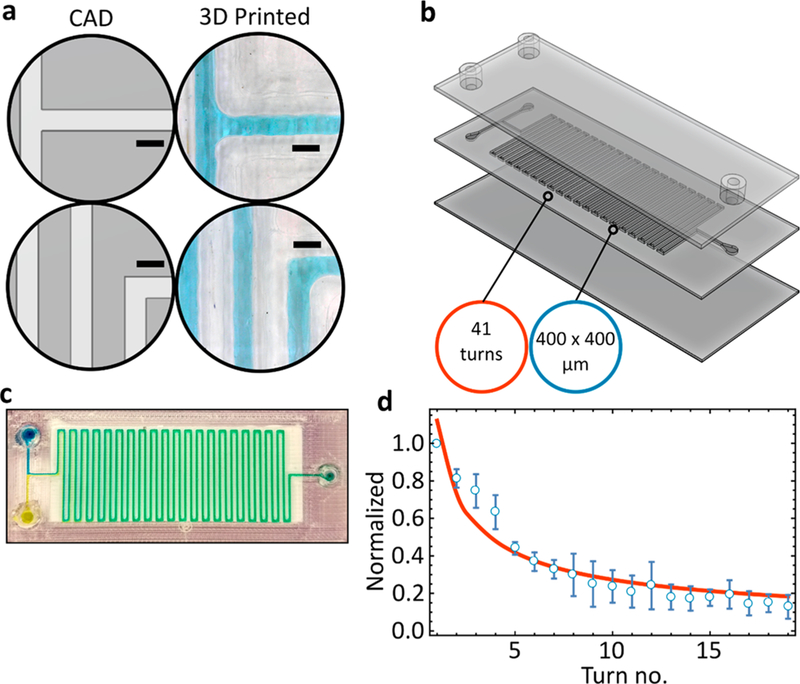
Tracking intensity changes. (a) CAD designed versus 3D printed channels. (b) One-step 3D printed serpentine mixer. (c) Image of yellow and blue dye mixing within the serpentine device. (d) Mixing efficiency is measured across 19 channels and normalized based on standard deviation of RGB channels. Line of best fit is in orange. All scale bars are 0.5 mm. Printed with PETg-XT.
Whether observing a dye interface at the inlet or at the outlet (60 mm downstream), the gL2 transparency remains consistent (Figure 3b). Leak-free, efficient mixing was readily obtained within our 3D printed serpentine mixer (Figure 3c). Printing of well-defined, debris-free channels was simple and easily reproducible. Since the device does not require any assembly but is rather a single continuous print, the structure remains sealed. We tested this configuration of flow rates up to 10 mL/min for at least 30 min (our maximum pump flow rate) and did not observe any leaking. Next, we looked at the rate of mixing and whether small intensity changes would be easy to discern (Figure 3d). We utilize the relative mixing index28 to track changes in standard deviations across the red, green, and blue channels. The exponential decrease in standard deviation reveals steady, easily discernible interfacial mixing of the two dyes (Figure 3d).
Droplet Tracking.
We utilized a simple T-junction microfluidic device to create discrete, monodisperse populations of oil-in-water droplets (Figure 4a). The gL2 allows for direct, real time visualization of droplet formation, which we recorded and processed in an offline automated droplet tracking software. By tracking movement across several frames, droplet size, trajectory, velocity, and more can be obtained.27
Figure 4.
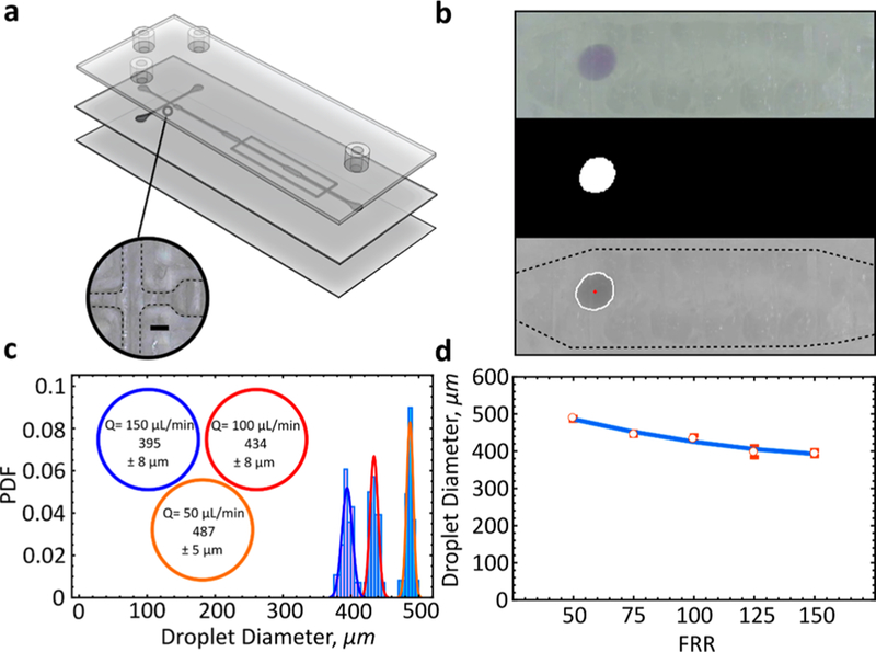
Droplet formation and tracking. (a) Device schematic with an image of the droplet formation junction. (b) Automated droplet tracking for velocity and size characterization. The 3D printed transparent layer is barely visible and does not interfere with droplet tracking software obtained from a third party. (c) Oil-in-water droplet distribution as a function of flow rate. PDF, probability density function. Size is shown as mean ± s.d. (d) Droplet size as a function of flow rate ratio (FRR) where the inlet is kept constant (Q = 1 uL/ min). Size is shown as mean ± s.d. Printed with PETg-XT. Scale bar, 0.5 mm.
Typically, transparent FDM devices contain distinct artifacts between adjacent extruded layers that can result in interference with automated tracking and poor characterization (Supplementary Figure S7). We show that not only does the gL2 surface not interfere with any of the automated tracking processes but that the channels are well-formed, and droplet tracking readily follows (Figure 4b).
Automated droplet tracking reveals the formation of monodisperse droplets across a range of flow rates (Figure 4c). By simply adjusting the continuous phase flow rate from 50 to 150 μL/min, droplet populations ranging in size from 487 ± 5 (0.487 μL) to 393 ± 8 (0.393 μL) μm can be created (Figure 4d). As expected, an increase in the FRR leads directly to a decrease in droplet diameter. The methodology and o/w droplets created here could be useful for preparing cosmetic and food products. We also demonstrate the formation of water-in-oil droplets without the addition of any surfactants. Droplets can be readily formed at high flow rates (∼2 mL/ min) and imaged with a high-speed camera (Supplementary Figure S8). Further, we show that embedding channels within a microfluidic chip for 3D-droplet formation is possible. Depending on the design, no modifications to the protocols presented here are necessary for creating embedded channels (Supplementary Figure S9).
DNA Melting Analysis.
One important application enabled by our transparent, heat-resistant, 3D printed microfluidic device is on-chip DNA melting analysis. This assay has the ability to identify different sequences of DNA by observing their unique, temperature-dependent melting profiles from the double-stranded to the single-stranded state (based on their unique ratio of C–G to A–T bonds).29 To enable DNA melting analysis, the fluorescent marker LCGreen is added to the DNA mixture. The marker fluoresces only in the presence of double-stranded DNA such that, when the DNA melts, the measured fluorescent signal drops off steeply. As a proof-of-concept, we first describe how to manufacture heat-resistant microfluidic devices followed by a demonstration of spatial DNA melting analysis in the presence of a thermal gradient (Figure 5a).
Figure 5.
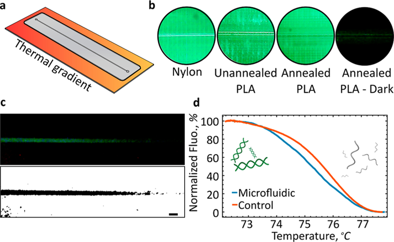
DNA melting analysis. (a) Schematic of an annealed PLA device with an embedded 400 by 400 μm channel exposed to a linear thermal gradient. (b) Autofluorescence as a function of material and annealing. CC-PLA, once annealed and shaded with a marker (Annealed PLA-Dark), allowed for rapid visualization of fluorescence emitted by the sample. (c) Fluorescence emission under an applied spatial thermal gradient. Fluorescence was enhanced for clarity. Thresholding clearly reveals temperature dependence. (d) Normalized fluorescence and Tm of the DNA was comparable between the 3D printed chip developed in this work and a commercial instrument (HR-1). Scale bar, 1 mm.
Here, we present a simple strategy for annealing thin microfluidic devices embedded with a single 400 × 400 μm channel. PLA devices exhibit several modes of deformation when placed onto the surface of a preheated hot plate set at a temperature far above the glass transition temperature (Supplementary Figure S10a). The most severe outcome is the rapid warping of the microfluidic device, transforming into a U-shaped structure. In contrast, annealed devices exhibit little deformation and maintain a perfectly rigid structure. While undergoing slight channel deformation and warping, annealed devices retain their initial geometries (Supplementary Figure S10b,c). Unannealed PLA devices are not compatible with thermal applications equal to or greater than the glass transition temperature of the material (∼67 °C for CC-PLA). Utilizing unannealed PLA devices at temperatures required for PCR (95 °C) will result in immediate deformation. We observe typical deformations for unannealed devices (Supplementary Figure S10d) of 7.48 and 0.78 mm for annealed devices (Supplementary Figure S10e). While slight warping is observed for annealed devices, the changes are subtle and do not interfere with device operation or downstream reaction quantification.
Initially, Nylon-680 is used for constructing microfluidic chips for melting analysis because of its high glass transition temperature. However, significant autofluorescence was observed within the channel upon illumination with blue filtered light (Figure 5b). Devices made from Crystal Clear PLA result in the least channel interference (Supplementary Figure S11). We found that annealing of the device decreases the noise associated with autofluorescence measured along the channel length and significantly increases the signal-to-noise ratio within the collection channel. In order to further enhance the signal of the collected data across the channel, chip surfaces inside of the imaging region but away from the channel are blackened with a marker (shown as Annealed PLA - Dark in Figure 5b).
In order to form a thermal gradient across the microfluidic chip, the chip is placed on top of a steel bridge that spans two copper heaters (Supplementary Figure S12). The steel plate, which reaches thermal equilibrium in minutes and is capable of maintaining a linear thermal gradient, was selected and validated based on COMSOL simulations (Supplementary Figure S13). The microfluidic chip placed on top of the thermal bridge does not impact the thermal gradient across the bridge (Supplementary Figure S14). The relatively small thickness of the microfluidic chip results in rapid temperature equilibration.
By placing a microfluidic chip loaded with DNA mixture across this gradient, we are then able to correlate the thermal and fluorescence data and to generate the melting curve shown in Figure 5d. The acquired melt has the features that we would expect: a linear region (owing to the LCGreen’s inherent temperature dependence), a steep region (where the DNA is melting), and another linear region past the melt. The melting temperature (Tm) of DNA obtained using our 3D printed chip closely matched that of a commercially available instrument (∼75.3 vs ∼75.7 °C). It should be noted that PLA-based devices are not compatible with high pH assays.
CONCLUSIONS
We have utilized affordable, commercially available FDM-based 3D printers to print, sealed, assembly free microfluidic devices. We tested four types of printable materials and characterized them specifically for rapid fabrication of microfluidic devices. Furthermore, we have shown that affordable polymer materials can be used to print glass-like layers (gL2) that facilitate optical visualization of fluids in printed microfluidic devices. We successfully demonstrate two applications of microfluidics in our 3D printed microfluidic devices: droplet generation and tracking and identification of DNA using DNA melting analysis. Specifically, for DNA melting analysis, we demonstrate that annealing 3D printed microfluidic devices can make them suitable for high-temperature applications. In this case, we characterize material deformation (during annealing) of CC-PLA and show reduction in autofluorescence due to annealing. Further, we provide a troubleshooting guide for commonly encountered problems during 3D printing and provide print recipes for the materials utilized in this study.
As a result of a number of affordable FDM-based 3D printers available commercially, we believe it is important to explore the full capabilities of these printers for microfluidic device fabrication. The resolution of such printers is still limited to 250–300 μm for repeatable fabrication of open microfluidic channels, without any supporting structures. Regardless, the ease and cost-effectiveness of printing micro-fluidic systems with FDM-based 3D printers offers significant advantages for rapid research and commercial microfluidic device fabrication.
Supplementary Material
ACKNOWLEDGMENTS
AF acknowledges funding by a Faculty Scholar grant from the Howard Hughes Medical Institute, the Searle Scholars Program, NIH grant 1DP2GM110772-01, and the Chan Zuckerberg Biohub. Further, AF acknowledges funding by the National Institutes of Health (P50 GM082545). AJ acknowledges funding by the Graduate Research Fellowship, NSF grant 1747505.
Footnotes
ASSOCIATED CONTENT
Supporting Information
The Supporting Information is available free of charge on the ACS Publications website at DOI: 10.1021/acs.analchem.8b02356.
Contains printing parameters, troubleshooting guide, extended methods section, and figures characterizing transparency, droplet formation, annealing, and DNA melting experimentation (PDF)
Contains the .ini files for all materials used in the study. These files contain all printing parameters and can be directly loaded into Slic3r (ZIP)
The authors declare no competing financial interest.
REFERENCES
- (1).Di Carlo DD; Irimia D; Tompkins RG; Toner M Proc. Natl. Acad. Sci. U. S. A 2007, 104 (48), 18892–18897. [DOI] [PMC free article] [PubMed] [Google Scholar]
- (2).Teh S-Y; Lin R; Hung L-H; Lee AP Lab Chip 2008, 8 (2), 198–220. [DOI] [PubMed] [Google Scholar]
- (3).Nie Z; Li W; Seo M; Xu S; Kumacheva E J. Am. Chem. Soc 2006, 128 (29), 9408–9412. [DOI] [PubMed] [Google Scholar]
- (4).Halldorsson S; Lucumi E; Gómez-Sjöberg R; Fleming RMT Biosens. Bioelectron 2015, 63, 218–231. [DOI] [PubMed] [Google Scholar]
- (5).Gorkin R; Park J; Siegrist J; Amasia M; Lee BS; Park J-M; Kim J; Kim H; Madou M; Cho Y-K Lab Chip 2010, 10 (14), 1758–1773. [DOI] [PubMed] [Google Scholar]
- (6).Tseng P; Murray C; Kim D; Di Carlo DD Lab Chip 2014, 14 (9), 1491–1495. [DOI] [PubMed] [Google Scholar]
- (7).Bartholomeusz DA; Boutte RW; Andrade JD J. Microelectromech. Syst 2005, 14 (6), 1364–1374. [Google Scholar]
- (8).Carrilho E; Martinez AW; Whitesides GM Anal. Chem 2009, 81 (16), 7091–7095. [DOI] [PubMed] [Google Scholar]
- (9).Waheed S; Cabot JM; Macdonald NP; Lewis T; Guijt RM; Paull B; Breadmore MC Lab Chip 2016, 16 (11), 1993–2013. [DOI] [PubMed] [Google Scholar]
- (10).Pham DT; Gault RS Int. J. Mach. Tools Manuf 1998, 38 (10), 1257–1287. [Google Scholar]
- (11).Au AK; Huynh W; Horowitz LF; Folch A Angew. Chem., Int. Ed 2016, 55 (12), 3862–3881. [DOI] [PMC free article] [PubMed] [Google Scholar]
- (12).Ho CMB; Ng SH; Li KHH; Yoon Y-J Lab Chip 2015, 15 (18), 3627–3637. [DOI] [PubMed] [Google Scholar]
- (13).Lee JM; Zhang M; Yeong WY Microfluid. Nanofluid 2016, 20 (1), 5. [Google Scholar]
- (14).Urrios A; Parra-Cabrera C; Bhattacharjee N; Gonzalez-Suarez AM; Rigat-Brugarolas LG; Nallapatti U; Samitier J; DeForest CA; Posas F; Garcia-Cordero JL; et al. Lab Chip 2016, 16 (12), 2287–2294. [DOI] [PMC free article] [PubMed] [Google Scholar]
- (15).Ji Q; Zhang JM; Liu Y; Li X; Lv P; Jin D; Duan H Sci. Rep 2018, 8 (1), 4791. [DOI] [PMC free article] [PubMed] [Google Scholar]
- (16).Johnson TJ; Ross D; Locascio LE Anal. Chem 2002, 74 (1), 45–51. [DOI] [PubMed] [Google Scholar]
- (17).deMello AJ Nature 2006, 442, 394–402. [DOI] [PubMed] [Google Scholar]
- (18).Morgan AJL; Hidalgo San Jose L; Jamieson WD; Wymant JM; Song B; Stephens P; Barrow DA; Castell OK PLoS One 2016, 11 (4), e0152023. [DOI] [PMC free article] [PubMed] [Google Scholar]
- (19).Tsuda S; Jaffery H; Doran D; Hezwani M; Robbins PJ; Yoshida M; Cronin L PLoS One 2015, 10 (11), e0141640. [DOI] [PMC free article] [PubMed] [Google Scholar]
- (20).Bishop GW; Satterwhite JE; Bhakta S; Kadimisetty K; Gillette KM; Chen E; Rusling JF Anal. Chem 2015, 87 (10), 5437–5443. [DOI] [PMC free article] [PubMed] [Google Scholar]
- (21).Zhang JM; Li EQ; Aguirre-Pablo AA; Thoroddsen ST RSC Adv 2016, 6 (4), 2793–2799. [Google Scholar]
- (22).Ye B; Xu H; Bao B; Xuan J; Zhang L RSC Adv 2017, 7 (77), 48826–48834. [Google Scholar]
- (23).Zhang JM; Aguirre-Pablo AA; Li EQ; Buttner U; Thoroddsen ST RSC Adv 2016, 6 (84), 81120–81129. [Google Scholar]
- (24).Macdonald NP; Cabot JM; Smejkal P; Guijt RM; Paull B; Breadmore MC Anal. Chem 2017, 89 (7), 3858–3866. [DOI] [PubMed] [Google Scholar]
- (25).Sher D Dolomite’s Fluidic Factory 3D Prints $1 Microfluidic Chips https://3dprintingindustry.com/news/dolomites-fluidic-factory-3d-prints-1-microfluidic-chips-60883/ (accessed Jan 15, 2018).
- (26).Li F; Macdonald NP; Guijt RM; Breadmore MC Anal. Chem 2017, 89 (23), 12805–12811. [DOI] [PubMed] [Google Scholar]
- (27).Basu AS Lab Chip 2013, 13 (10), 1892–1901. [DOI] [PubMed] [Google Scholar]
- (28).Hashmi A; Xu J J. Lab. Autom 2014, 19 (5), 488–491. [DOI] [PubMed] [Google Scholar]
- (29).Reed GH; Kent JO; Wittwer CT Pharmacogenomics 2007, 8 (6), 597–608. [DOI] [PubMed] [Google Scholar]
Associated Data
This section collects any data citations, data availability statements, or supplementary materials included in this article.


