

We report 3D printing of anisotropically polarized optical devices composed of perovskite nanowire-block copolymer composites.
Abstract
One-dimensional (1D) nanomaterials with highly anisotropic optoelectronic properties are key components in energy harvesting, flexible electronics, and biomedical imaging devices. 3D patterning methods that precisely assemble nanowires with locally controlled composition and orientation would enable new optoelectronic device designs. As an exemplar, we have created and 3D-printed nanocomposite inks composed of brightly emitting colloidal cesium lead halide perovskite (CsPbX3, X = Cl, Br, and I) nanowires suspended in a polystyrene-polyisoprene-polystyrene block copolymer matrix. The nanowire alignment is defined by the programmed print path, resulting in optical nanocomposites that exhibit highly polarized absorption and emission properties. Several devices have been produced to highlight the versatility of this method, including optical storage, encryption, sensing, and full-color displays.
INTRODUCTION
Semiconducting nanowires have unique anisotropic optoelectronic properties that arise from quantum (1) and dielectric (2) confinement effects, making them attractive candidates for a broad range of electronic and photonic applications (3–5). The ability to precisely pattern one-dimensional (1D) nanomaterials with controlled spatial orientation into planar and 3D structures that exhibit highly anisotropic properties (6) would open new avenues for the integrated design and assembly of optoelectronic devices (7, 8). Of the multiple types of semiconducting nanowires reported to date (5, 9, 10), cesium lead halide (CsPbX3, X = Cl, Br, and I) nanowires with a perovskite crystal structure (11, 12) offer several advantages for optoelectronic applications (Fig. 1, A to C). Unlike conventional colloidal semiconducting nanocrystals that typically require a core-shell structure to achieve high photoluminescence (PL) quantum yield, lead halide perovskite nanocrystals are ultra-bright and exhibit near-unity quantum yield without an encapsulating shell (13, 14). Through facile room temperature anion-exchange reactions, their halide composition and bandgap can be modified after synthesis, resulting in bright and tunable emission over the entire visible spectral range (Fig. 1B, figs. S1 and S2, and tables S1 and S2) (15, 16). Moreover, perovskite nanowires can be prepared with high aspect ratios (~100), resulting in polarization anisotropy due to a strong dielectric confinement effect (17). Given these unique properties combined with high quantum yields of up to 80%, perovskite nanowires are a potential candidate for several optoelectronic applications, including active layers for liquid crystal display (LCD) backlighting (3, 18), spectrum splitting (19), polarized photodetectors (2), and optically pumped lasers (4).
Fig. 1. Perovskite nanowire–block copolymer supramolecular nanocomposites.
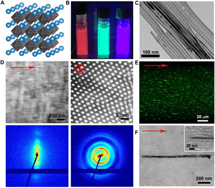
(A) Schematic diagram of the perovskite crystal structure. (B) PL of CsPbX3 (X = I, Br, and Cl) perovskite nanowires in toluene solution. Halide composition determines the material’s bandgap and color of emitted light (λexcitation = 380 nm). (C) TEM images of naturally aligned bundles of CsPbBr3 perovskite nanowires (length, ~1 μm; diameter, ~10 nm). (D) TEM images (top) and SAXS measurements (bottom) of the pure SIS filaments without nanowires printed using 1-mm-diameter nozzle (left, horizontally printed sample; right, filament cross sections), demonstrating microphase separated SIS hexagonal domains with long-range order and anisotropy. Red arrow indicates printing and the microdomain alignment direction. (E) A maximum intensity projection of z-stack fluorescence confocal image of the printed nanowire-block copolymer filament (diameter, 100 μm; λexcitation = 365 nm). (F) Representative TEM images of nanocomposite filaments printed using 1-mm-diameter nozzle showing perovskite nanowires oriented in parallel with the print direction and locally conform to the SIS block copolymer microdomains. A higher-magnification TEM image (inset) shows that nanowires primarily segregate to PI-rich domains (see also fig. S6 and table S4). The TEM samples in (D) and (F) are sectioned using cryo-ultramicrotome and stained with OsO4, which selectively darkens the PI domains.
To create optical nanocomposite devices, planar and 3D patterning methods are needed that allow localized control over the orientation of semiconducting nanowires embedded within polymer matrices (20, 21). Most patterning methods explored to date, such as mechanical stretching (3), fluid flow (22), Langmuir-Blodgett (23), contact printing (24), nanocombing (20), and electrospinning (25), are multistep processes that are limited to unidirectional alignment. Srivastava et al. (26) recently reported the self-assembly of CdSe/CdS nanorods on a prealigned molecular template. Although this approach leads to omnidirectional alignment in-plane, it is limited to specific surface chemistries. We recently demonstrated that shape-morphing architectures composed of aligned cellulose fibrils embedded within a hydrogel matrix can be fabricated by direct ink writing (DIW), an extrusion-based 3D-printing method (6). Unlike electrospinning and photoalignment, DIW enables exquisite control over anisotropic filler alignment within complex 3D architectures. However, its general applicability for patterning functional architectures, such as photonic devices, has yet to be explored.
Here, we report the design, printing, and characterization of polarized optical architectures composed of perovskite nanowire–filled block copolymer matrices in several device motifs. As an exemplar, we developed a nanocomposite ink composed of perovskite nanowire bundles suspended in a cylindrical microphase-forming polystyrene-polyisoprene-polystyrene (SIS) block copolymer matrix. During printing, the SIS block copolymer undergoes shear-induced alignment and forms macroscopically ordered cylindrical microdomains that enhance nanowire alignment along the printing direction (27). The modularity of this nanocomposite ink design should enable other anisotropic materials, e.g., metallic, semiconducting, and dielectric nanowires and block copolymers, to be programmably patterned by this method (28).
RESULTS
Our nanocomposite ink is created by mixing solutions of colloidal perovskite nanowires and SIS block copolymer in toluene. By varying the SIS concentration, we formed inks composed of ~0.05 weight % (wt %) nanowires that exhibit the requisite shear-thinning behavior and viscoelastic response needed for DIW (fig. S4). The nanowires are coated with an 18-carbon long alkyl chain ligand to promote their dispersion in toluene and, ultimately, their segregation to the hydrophobic polymer domains, yielding an environmentally stable nanocomposite. While macroscopic ordering of block copolymers by unidirectional mechanical alignment has been demonstrated previously (29), we show that it is also possible to control the orientation of the block copolymer microdomains through 3D printing. As evident from transmission electron microscopy (TEM) and small-angle x-ray scattering (SAXS) measurements (Fig. 1D), the printed SIS block copolymer filaments reveal strong evidence of ordered hexagonal microdomains, with d-spacing of ~26.5 nm and Herman’s orientation parameters of 0.53 to 0.77, over a broad range of nozzle sizes (diameter = 0.05 to 4.0 mm) (fig. S5). The printed SIS-CsPbBr3 nanocomposites also reveal that encapsulated nanowires are highly aligned along the print direction (Fig. 1, E and F, and fig. S6, A and B), predominantly residing within the polyisoprene (PI)–rich domains. This observation is not surprising given the respective Hildebrand solubility parameters and surface energies of the nanowire ligands, polystyrene (PS) and PI (table S4). By contrast, the nanowires and SIS microdomains are randomly oriented in control samples produced by bulk casting (fig. S6, C and D).
The shear-induced alignment of nanowire and SIS species coupled with the geometric confinement imposed by the SIS supramolecular architecture enables the programmable nanowire orientation within the printed optical composites, which influences their polarized and angular emission. We use Fourier imaging to map the angular emission of green-emitting CsPbBr3 nanowires (λemission = 517 nm) within the nanocomposites. The angular emission pattern of an individual nanowire is a strong function of its alignment and local dielectric environment (30). A horizontally aligned nanowire will have mostly horizontal dipole contributions, making bright lobes that are brightest at angles perpendicular to the dipole axis (31). By contrast, a vertically aligned dipole will be symmetric about the azimuthal angle, φ, due to its rotational symmetry. Figure 2A shows representative Fourier images of single perovskite nanowire bundles in the nanocomposite printed using a 50-μm-diameter nozzle. For a horizontally printed nanocomposite filament (Fig. 2A, left), the Fourier patterns show a symmetric pattern oriented along the left-to-right axis with two bright lobes at the top and bottom of the image, indicating that most of the dipole contributions are horizontally aligned along the printing axis. For comparison, the Fourier image from a vertical filament (Fig. 2A, right) presents a symmetric pattern about φ, indicative of mostly vertically oriented dipoles. Fitting these data reveals that 60 ± 6% of the dipoles in the aligned bundles are parallel to the direction of printing, yielding a highly anisotropic emission pattern for horizontal filamentary features (figs. S9 and S10) (32).
Fig. 2. Polarized emission from printed perovskite nanocomposites.
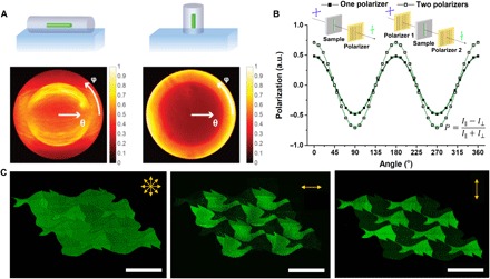
(A) Fourier images showing the angular emission from a nanowire bundle in the printed filament. Polar angle (θ) is plotted radially from 0° (center) to 70° (outer edge). Azimuthal angle (φ) is plotted around the circle starting at the right-hand side. Fourier image of a horizontal (left) and a vertical (right) filament on glass slide (cartoons, top). Angular emission pattern shows alignment of nanowires along filament axis. (B) Polarized emission of printed nanowire composites, measured using one linear polarizer installed in the emission path and two linear polarizers installed in both the excitation and emission paths. a.u., arbitrary units. (C) Artistic example of printed composites using their polarized emission (adapted from M. C. Escher, Sky and Water I art). Different parts are revealed for (left) no polarization, (middle) horizontal polarization, and (right) vertical polarization. Scale bars, 1 mm.
Next, we fabricated macroscopically polarized films with unidirectionally aligned CsPbBr3 perovskite nanowires that show a periodic (cos2θ) dependence on angle with an emission polarization ratio, , using a 50-μm nozzle. The degree of alignment achieved, albeit lower than desired, is comparable to other patterning methods (table S5). P can be enhanced to 0.71 ± 0.03 using a pair of polarizers, one in the excitation path and the other in the emission path (Fig. 2B). Additional emission polarization measurements from filaments printed using different nozzle sizes are shown in figs. S7 and S11. As a control, we also printed nanocomposites from inks composed of PS (Mp = 700 kDa) at the same polymer concentration in toluene (fig. S4) and compared their degree of polarization. Not unexpectedly, the printed SIS-CsPbBr3 perovskite nanowire features exhibited consistently higher polarization ratios than those composed of pure PS (fig. S11) due to microdomain confinement effects (27). Figure 2C shows direct writing of these nanowire-block copolymer inks in the form of an Escher-inspired image. The as-printed structure uniformly emits green light (left). However, when viewed using polarizers, swans (middle, horizontal polarization) or fish (right, vertical polarization) emerge due to differences in nanowire alignment, which vary orthogonally between printed features.
The ability to digitally program polarization anisotropy in 3D-printed nanocomposites may open new avenues for optical device fabrication. As one example, we fabricated a 3-bit grayscale image consisting of 200 μm × 200 μm size square-shaped pixels (Fig. 3A). We achieved different grayscale intensities by printing SIS-CsPbBr3 nanocomposites oriented along eight different directions corresponding to eight equally spaced polarization-dependent PL intensities (Fig. 3A, right). These patterned architectures serve as optical memories for write once–read many (WORM) times devices. In addition, these architectures may be suitable for security encryption, i.e., the patterned image can be readily encrypted without using a polarizer or switching off the excitation. Encryptable memories in more complex motifs can be obtained by printing multilayer architectures, in which each layer stores different optical information. For example, two orthogonally printed patterns emerge sequentially as one views the bilayer photonic hologram using a pair of polarizers that switched from the horizontal to vertical direction (Fig. 3B). To extend this concept, we patterned the letters “L-I-G-H-T” within a five-layer device, each of which is viewed at different heights (fig. S12). Using embedded 3D printing (33), an emerging variant of direct writing in which inks are printed omnidirectionally within a viscoplastic matrix, we printed the letters “H” and “I” in random orientations. Using polarized ultraviolet (UV) light illumination, each of these letters can be selectively viewed through the transparent matrix using a polarizer at the appropriate angle (fig. S13).
Fig. 3. Polarized perovskite nanocomposites via 3D printing.
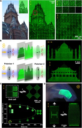
(A) A photo (left) is downsized to a 3-bit grayscale image consisting of 60 (w) × 90 (h) square-shaped pixels (left, inset). Taking advantage of the polarization angle–dependent emission intensities, we convert the grayscale intensities to eight different printing directions (top right) and print the image (middle). (B) Polarization holograms. When viewed using a pair of linear polarizers, the two-layer device projects an image of Taj Mahal (horizontally printed, horizontal polarization) and Forbidden City (vertically printed, vertical polarization). (C and D) A mechano-optical metamaterial based on an auxetic structure. (C) The unit cell (top) consists of four rotating squares, which can rotate up to 45°. The polarization-dependent emission results in a strain-intensity relationship (bottom). (D) This structure is flexible and can adhere to a finger (top). Undergoing reversible stretching motions, the digitally patterned H letter (printed in vertical direction and in parallel with the polarizers) is displayed (left) or encrypted (right).
To further demonstrate the versatility of this approach, we created optical strain sensors based on an auxetic structure composed of rotating square regions. This mechano-optical device exhibits the unusual mechanical property of a negative Poison’s ratio and a strain-dependent optical response due to its unique subunit structure. When stretched uniaxially, the four square-shaped motifs within a unit cell rotate up to 45° from their original positions. Their polarization-dependent emission results in a well-defined strain-intensity relationship (Fig. 3C, bottom). Printed in two orthogonal directions in an unstretched state, we demonstrate that an emission pattern—H letter—can be encrypted upon stretching (Fig. 3D). We envision the ability to create dynamic camouflage in skin-like motifs, in which different optical patterns emerge and disappear upon mechanical stretching.
RGB (red, green, and blue) quantum dots have been widely investigated for color mixing. Through anion-exchange reactions (15), we obtained halide perovskites composed of red-emitting CsPb(Br0.2I0.8)3 (λemission = 660 nm) and blue-emitting CsPb(Br0.2Cl0.8)3 (λemission = 450 nm) nanowires. These nanowires exhibit similar shapes, sizes, and polarized optical properties akin to the green-emitting CsPbBr3. When individually printed in the form of unidirectionally ordered films, the nanocomposites serve as polarized photon downshifters (Fig. 4A). For example, we used multimaterial 3D printing to create a polarizer tunable multiplexed color display. While we recognize that perovskite nanowires are not yet optimal materials for display applications, this demonstration serves to highlight the programmable control over nanowire composition and alignment afforded by digital assembly. Specifically, we fabricated a basic RGB pixel composed of three hexagonal tiles that are patterned with 60° difference in their respective printing directions (Fig. 4C, inset). Next, we fabricated a 10 × 10 multiplexed RGB pixel array using the basic repeating unit. The fluorescent images from the same pixel array upon the rotation of polarization is presented in Fig. 4B. The red, green, and blue colors are obtained when the polarizers are parallel to the print directions of the three corresponding hexagonal tiles, whereas the mixed colors of yellow (red + green), purple (red + blue), and cyan (blue + green) are achieved when the polarizers are positioned at 30° to the print directions of the two primary contributing pixels and perpendicular to that of the third.
Fig. 4. Polarizer tunable color multiplexing.
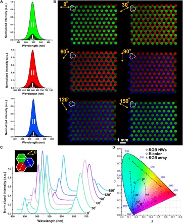
(A) Polarized PL spectra of the printed nanocomposites incorporating CsPbBr3 (green), CsPb(Br0.2I0.8)3 (red), and CsPb(Br0.2Cl0.8)3 (blue) nanowires, taken with a pair of two linear polarizers installed in both the excitation and emission paths. (B) Optical images of printed pixel arrays showing polarization-dependent emission multiplexing. Images are taken using a multiphoton microscope with a polarized excitation source and with a linear polarizer in the emission path. (C) Spectral emission profiles of the pixel array based on hexagonal tiles of red, green, and blue light-emitting perovskite nanocomposites printed along three directions oriented with a 60° difference upon rotating both polarizers. (D) Its corresponding colors on CIE 1931 chromaticity diagram (right). Two types of potential display operations are presented (see also figs. S14 and S15). The solid line and triangles represent colors using the multiplexed RGB pixel arrays in (B). NWs, nanowires. The dashed lines and circles represent the multiplexed RG, RB, and GB pixel arrays printed in two orthogonal directions shown in fig. S14.
Figure 4C presents polarizer tunable spectral responses of the multiplexed RGB array and its corresponding chromaticity range on the CIE (Commission on Illumination) 1931 diagram (Fig. 4D, solid line and triangles). While a smaller range is achieved on the CIE chart compared to the state-of-the-art LCDs, our printed displays offer a remarkably simple design to achieve color tunability. By fabricating three bicolor pixel arrays using two orthogonally printed nanowire composites, R + G, G + B, and B + R (Fig. 4D, dashed lines and circles, and figs. S14 and S15), further improvements are obtained. Unlike LCDs that rely on conventional quantum dot color filters (34) composed of a polarizer coupled with a nonpatterned quantum dot film, our printed films use direct polarized photon downshifters, i.e., “active” color filters. However, further improvements in both nanowire synthesis and printing are needed to yield higher efficiencies for display applications.
DISCUSSION
In summary, we have shown that direct writing of nanocomposite inks composed of perovskite nanowire–filled block copolymer matrices enables patterning of optoelectronic devices in myriad motifs. By deterministically programming both nanowire composition and alignment, we have created optical nanocomposites for applications that include information storage and encryption, mechano-optical sensing, and optical displays. Our findings provide a new avenue for the rapid design and manufacturing of functional devices composed of anisotropic building blocks encapsulated within soft polymeric matrices.
MATERIALS AND METHODS
Nanowire synthesis and characterization
The following chemicals were used as received without further purification: Cs2CO3 (99.9%; Aldrich), octadecene (ODE; 90%; Aldrich), oleic acid (OA; 90%; Aldrich), PbBr2 (99.999%; Alfa Aesar), PbI2 (99%; Aldrich), oleylamine (OAm; 70%; Aldrich), octylamine (OCT; 99%; Aldrich), and hexane (99.9%; Fisher Scientific). First, Cs-oleate solutions were prepared similar to the reported approach developed by Protesescu et al. (14). Briefly, 0.2 g of Cs2CO3 and 0.6 ml of OA were loaded into a three-neck flask along with 7.5 ml of ODE, degassed and dried under vacuum at 120°C for 20 min, and then heated under N2 to 150°C until all Cs2CO3 reacted with OA. Next, CsPbBr3 nanowires were synthesized by loading 28 ml of ODE and 0.2 mmol PbX2 into a three-neck flask and degassing under vacuum for 20 min at 120°C. Dried OCT (2.6 ml) and dried OAm (2.6 ml) were injected at 120°C under N2 successively. The temperature was raised to 135°C, and the solution was stirred for 20 min. Unlike the Protesescu et al. (14) synthesis, this solution remains opaque and does not fully complex. This difference is important for the growth of high-quality wires. The solution was kept at 135°C, and 2.8 ml of as-prepared Cs-oleate solution was quickly injected. After 60 min, the reaction mixture was cooled by an ice-water bath. The nanowires were isolated by centrifugation at 6000 rpm for 5 min and washed once with hexane, and the obtained precipitated nanowires were redispersed in toluene for further use.
The perovskite nanowires were surface-treated following this protocol. First, anhydrous toluene (5 ml), PbBr2 (0.188 mmol; X = Cl or Br), OA (0.5 ml), and OAm (0.65 ml) were added to a scintillation vial within an argon inert atmosphere glove box. The solution was then stirred at 100°C within the glove box until the complete dissolution of the PbBr2 salt occurs, which may take several hours. The resulting concentrated stock solution was stable at room temperature, but it was stored in a glove box. The cleaned nanowire solution was then mixed with the above solution and stirred at 85°C until the solution turns turbid. The nanowires were isolated by centrifugation at 6000 rpm for 5 min and redispersed in toluene for further use. Figure S1 demonstrates the improvement in PL quantum yield (PLQY) due to surface treatment using different volumetric ratios of the added solution to a colloidal suspension with an optical density of ~1. A two–order of magnitude increase in quantum yield was demonstrated at a volumetric ratio of ~1:1. Higher ratios of the precursor solution did not improve that value. Table S1 provides the PLQY of the perovskite nanowires used in our work.
Anion-exchange reactions were performed under air-free conditions using standard Schlenk techniques. PbX2 as the anion source was mixed with ODE (5 ml) in a three-neck flask and kept under vacuum at 100°C for 20 min. OA (0.6 ml) and OAm (0.6 ml) were injected at 100°C under N2 gas flow. After complete dissolution of the anion source, the temperature was lowered to 40° to 80°C, and CsPbBr3 nanowires (0.01 to 0.025 mmol) dispersed in toluene were injected to initiate the anion-exchange reaction. After reaction, the nanowires were isolated by centrifugation at 6000 rpm for 5 min and washed once with hexane. The precipitated nanowires were then redispersed in toluene for further analysis. To maintain their high quantum yield, the nanowires were kept in dry and air-free conditions during and after the exchange process. The stability of Cs(PbBr0.2I0.8)3 is described in table S2.
To characterize the perovskite nanowires, we used TEM images and high-resolution TEM. TEM images were taken with a FEI Tecnai TEM at an accelerating voltage of 200 kV. We also measured their luminescence quantum yield using a homebuilt integrating sphere spectrofluorometer.
Nanocomposite inks
SIS (432415) and toluene were acquired from Sigma-Aldrich. Pure PS with different molecular weights was purchased from Alfar Aesar. All materials were used as received without further modification. Nanocomposite inks were created by combining 50 wt % SIS (or PS) with toluene, to which 0% or 0.05 wt % nanowires were added. A brief (~10 min) sonication step was performed to enhance the nanowire dispersion in the polymer solutions. The inks were loaded into a SpeedMixer DAC 400 planetary mixer (FlackTek, Landrum, SC) and spun at 2000 rpm for 15 min.
Direct ink writing
Print paths were generated via G-code, which outputs the XYZ motion of the 3D printer (Aerotech). G-code was generated using MATLAB, Slic3r, and CIMCO. The inks were loaded into 3-ml luer-lock polypropylene syringes, which were placed in an HP7x high-pressure adapter and mounted to the head of a three-axis positioning stage (Aerotech Inc., Pittsburgh, PA). The inks were extruded through custom-pulled glass nozzles by applying a controlled air pressure via an Ultimus V pressure control box (Nordson EFD). The auxetic metamaterials were printed using glass nozzles with an inner diameter (ID) of 50 μm (printing speed, 1 mm/s) onto a substrate of the same dimension printed using a two-part silicone polydimethylsiloxane (PDMS) elastomer (SE 1700, Dow Chemical) with a 10:1 base to catalyst (by weight). A 0.4 wt % PEIE [80% solution of ethoxylated poly(ethylenimine), 35 to 40 wt % in H2O, average MW = 70,000; Sigma-Aldrich] was added to make the PDMS adherent (35). All other samples were printed using glass nozzles with an ID of ~20 μm (printing speed, 500 μm/s), except for the five-layer device (shown in fig. S12), which was printed using glass nozzles with an ID of ~10 μm (printing speed, 100 μm/s). All nanocomposite architectures were printed on glass coverslips spin-coated with a crystalbond-590 adhesion layer (thickness, ~1 μm).
Back focal plane imaging
The printed nanocomposites were imaged using a homebuilt inverted microscope equipped with an oil immersion objective (Nikon Plan Apo VC, 100×, numerical aperture = 1.4; oil: Cargille Immersion Oil Type FF, lot: 010780; n = 1.479), a tube lens (f = 200 mm), and an electron-multiplying charge-coupled device (EMCCD) camera (Andor iXon Ultra 897 EMCCD; T = −60°C). Specifically, samples printed using a 50-μm nozzle on glass coverslip were excited using a 405-nm continuous-wave diode laser (Thorlabs LP405-SF30), and their fluorescence (emission, ~515 nm) was passed through a dichroic mirror (Semrock FF414-Di01-25x36) and additional long-pass and bandpass filters to reduce the background signal (Semrock FF02-409/LP-25 and Thorlabs FB500-40). Nanowires within the printed nanocomposites were focused on, and then an additional lens (f = 250 mm) was added to the optical path between the objective and tube lens to image the Fourier space, as described previously (36). The exposure time was 2 to 3 s for each image, and the camera was operated in “conventional” mode (readout rate, 3 MHz). Further details and schematics are provided in fig. S8.
Optical characterization
The polarization dependence of the printed nanocomposites was characterized using a standard fluorospectrometer (Photon Technology International), with a polarizer (Thorlabs LPUV1000) mounted in the excitation path and a polarizer (Thorlabs LPVISE100-A) mounted in the emission path. Both polarizers were mounted on piezo-driven motorized rotation stages (Newport AG-PR100), and the polarization angles were controlled using a computer. The microscope image in Fig. 1E was taken using an upright confocal microscope (Zeiss LSM 710) with a 63× oil immersion objective. The excitation was provided by a UV light-emitting diode (LED) with an excitation wavelength of 365 nm without polarization. With the exception of Fig. 3B, all optical images in Figs. 2 to 4 and figs. S12 and S14 were taken using a Leica SP5 multiphoton inverted confocal microscope equipped with a linearly polarized, two-photon excitation source at a wavelength of 720 nm. A polarizer (Thorlabs LPVISE100-A) was custom-installed in the emission path. The rotation of polarization was achieved by rotating the samples. The optical images in Fig. 3B were taken with a fluorescence microscope (Zeiss Axio Observer) using a 5× objective. The excitation was provided using a UV LED with an excitation wavelength of 365 nm. A pair of polarizers (Thorlabs LPUV1000 and Thorlabs LPVISE100-A) was placed in the excitation and emission path.
Small-angle x-ray scattering
The SAXS system used a Rigaku 002 microfocus x-ray source with an osmic staggered parabolic multilayer optics to focus the beam crossover at the second pinhole. It has two sets of JJ x-ray 4 jaw collimation slits that are tunable from 0.02 to 1 mm. The printed nanocomposites were introduced into a large vacuum chamber that was pumped down to 0.08 mbar. The sample stage has x-y travel and theta tilt for grazing incidence SAXS measurements, and a Dectris PILATUS 300 K detector moves from 100 to 1500 mm from the sample.
Microstructural characterization
The printed nanocomposites were sliced into thin sections (70 to 100 nm thick) using cryo-ultramicrotome maintained at −120°C and then selectively stained with OsO4 to enhance phase contrast between the PI and PS domains. The TEM images in Fig. 1 (D and F) and fig. S6 were acquired using TEM (JEOL-1200EX) at an accelerating voltage of 80 kV.
Code availability
The G-code print paths for all nanocomposite architectures are available on request.
Supplementary Material
Acknowledgments
We thank C. Visser (Harvard), X. Wang (Harvard), N. Lin (Harvard), Y. Yao (Harvard), and B. Duncan (Lincoln laboratory) for the useful discussion. We thank J. Aizenberg at Harvard for the access to use polarized light microscope. We thank T. Farrante for assistance with optical imaging and M. Ericsson for the ultra-cryomicrotome TEM sample preparation. Funding: This work was supported by the DOE Light-Material Interactions in Energy Conversion Energy Frontier Research Center under grant DE-SC0001293. This work was performed, in part, at the Harvard University Center for Nanoscale Systems (CNS), a member of the National Nanotechnology Coordinated Infrastructure Network (NNCI), which is supported by the National Science Foundation under NSF ECCS award no. 1541959. This work also made use of the Shared Experimental Facilities supported, in part, by the MRSEC Program of the National Science Foundation (DMR-1419807). N.Z. was partially supported by Camille and Henry Dreyfus Postdoctoral Fellowship. C.N.E. was supported by the Office of Energy Efficiency & Renewable Energy Postdoctoral Fellowship Program. J.A.L. acknowledges the generous support of our work provided by the GETTYLAB. Y.B. acknowledges support from the Ministry of National Infrastructure, Energy and Water Resources in Israel as part of their postdoctoral fellowship program in leading universities abroad (funder name: Ministry of National Infrastructure, Energy and Water Resources; country: Israel; funder ID: 501100008991; award/grant no. 4501275884-216-01-012). Back focal plane imaging was performed at the Molecular Foundry and supported by the Office of Science, Office of Basic Energy Sciences, U.S. Department of Energy under contract no. DE-AC02-05CH11231. Author contributions: N.Z., Y.B., C.N.E., A.P.A., and J.A.L. conceived the experimental work. N.Z., Y.B., and C.N.E. led the experiments, with assistance from D.Z. and P.Y. N.Z., Y.B., C.N.E., A.P.A., and J.A.L. contributed to data analysis and interpretation and wrote the paper. All authors provided feedback. Competing interests: J.A.L. is a cofounder of Voxel8, which focuses on multimaterial 3D printing. N.Z., Y.B., A.P.A., and J.A.L. are inventors on a provisional patent application related to this work filed by Harvard University (no. 62/822,195, filed on 22 March 2019). The authors declare no other competing interests. Data and materials availability: All data needed to evaluate the conclusions in the paper are present in the paper and/or the Supplementary Materials. Additional data related to this paper may be requested from the authors.
SUPPLEMENTARY MATERIALS
Supplementary material for this article is available at http://advances.sciencemag.org/cgi/content/full/5/5/eaav8141/DC1
Fig. S1. Optical properties of CsPbBr3 nanowires.
Fig. S2. Nanowire absorption spectra.
Fig. S3. Stability of CsPb(Br0.2I0.8)3 nanowires.
Fig. S4. Nanocomposite ink rheology.
Fig. S5. SAXS measurements of SIS block copolymer inks.
Fig. S6. TEM images of printed and cast nanocomposites.
Fig. S7. Polarization dependence of printed nanocomposite filaments composed of inks containing 50 wt % SIS with 0.05 wt % perovskite nanowires as a function of printing speed.
Fig. S8. Fourier imaging setup.
Fig. S9. Fourier images of printed SIS-CsPbBr3 block copolymer nanocomposites.
Fig. S10. Measuring dipole alignment from Fourier images.
Fig. S11. Emission polarization of printed nanocomposite filaments.
Fig. S12. Five-layer photonic device showing “L-I-G-H-T” pattern imaged using polarized fluorescence microscopy along the z direction.
Fig. S13. Embedded 3D printing of perovskite nanowire ink in a transparent viscoplastic matrix housed within a cubic mold.
Fig. S14. Fluorescence images of printed pixel arrays showing polarization-dependent emission multiplexing using two nanowire composites printed in orthogonal directions.
Fig. S15. Schematics of different display operations presented in CIE 1931 diagram (Fig. 4D).
Table S1. Comparison of PLQY for different perovskite nanowires.
Table S2. Fluorescence stability of red-emitting CsPb(Br0.2I0.8)3 nanowires embedded in a polymer.
Table S3. Printing pressures used for patterning nanocomposite inks at varying nozzle sizes and print speeds.
Table S4. Hildebrand solubility and surface energies of species used to form nanocomposite inks.
Table S5. Comparison of different techniques for aligning semiconductor nanowires.
REFERENCES AND NOTES
- 1.Cao L., White J. S., Park J. S., Schuller J. A., Clemens B. M., Brongersma M. L., Engineering light absorption in semiconductor nanowire devices. Nat. Mater. 8, 643–647 (2009). [DOI] [PubMed] [Google Scholar]
- 2.Wang J., Gudiksen M. S., Duan X., Cui Y., Lieber C. M., Highly polarized photoluminescence and photodetection from single indium phosphide nanowires. Science 293, 1455–1457 (2001). [DOI] [PubMed] [Google Scholar]
- 3.Cunningham P. D., Souza J. B. Jr., Fedin I., She C., Lee B., Talapin D. V., Assessment of anisotropic semiconductor nanorod and nanoplatelet heterostructures with polarized emission for liquid crystal display technology. ACS Nano 10, 5769–5781 (2016). [DOI] [PubMed] [Google Scholar]
- 4.Robert R., Ploss D., Kriesch A., Buschlinger R., Geburt S., Peschel U., Ronning C., Polarization features of optically pumped CdS nanowire lasers. J. Phys. D 47, 394012 (2014). [Google Scholar]
- 5.Law M., Goldberger J., Yang P., Semiconductor nanowires and nanotubes. Annu. Rev. Mater. Res. 34, 83–122 (2004). [Google Scholar]
- 6.Sydney Gladman A., Matsumoto E. A., Nuzzo R. G., Mahadevan L., Lewis J. A., Biomimetic 4D printing. Nat. Mater. 15, 413–418 (2016). [DOI] [PubMed] [Google Scholar]
- 7.Kong Y. L., Tamargo I. A., Kim H., Johnson B. N., Gupta M. K., Koh T.-W., Chin H.-A., Steingart D. A., Rand B. P., McAlpine M. C., 3D printed quantum dot light-emitting diodes. Nano Lett. 14, 7017–7023 (2014). [DOI] [PubMed] [Google Scholar]
- 8.Saada G., Layani M., Chernevousky A., Magdassi S., Hydroprinting conductive patterns onto 3D structures. Adv. Mater. Technol. 2, 1600289 (2017). [Google Scholar]
- 9.Li Y., Qian F., Xiang J., Lieber C. M., Nanowire electronic and optoelectronic devices. Mater. Today 9, 18–27 (2006). [Google Scholar]
- 10.Koscher B. A., Bronstein N. D., Olshansky J. H., Bekenstein Y., Alivisatos A. P., Surface- vs diffusion-limited mechanisms of anion exchange in CsPbBr3 nanocrystal cubes revealed through kinetic studies. J. Am. Chem. Soc. 138, 12065–12068 (2016). [DOI] [PubMed] [Google Scholar]
- 11.Zhang D., Eaton S. W., Yu Y., Dou L., Yang P., Solution-phase synthesis of cesium lead halide perovskite nanowires. J. Am. Chem. Soc. 137, 9230–9233 (2015). [DOI] [PubMed] [Google Scholar]
- 12.Talapin D. V., Lee J.-S., Kovalenko M. V., Shevchenko E. V., Prospects of colloidal nanocrystals for electronic and optoelectronic applications. Chem. Rev. 110, 389–458 (2010). [DOI] [PubMed] [Google Scholar]
- 13.Imran M., di Stasio F., Dang Z., Canale C., Khan A. H., Shamsi J., Brescia R., Prato M., Manna L., Colloidal synthesis of strongly fluorescent CsPbBr3 nanowires with width tunable down to the quantum confinement regime. Chem. Mater. 28, 6450–6454 (2016). [DOI] [PMC free article] [PubMed] [Google Scholar]
- 14.Protesescu L., Yakunin S., Bodnarchuk M. I., Krieg F., Caputo R., Hendon C. H., Yang R. X., Walsh A., Kovalenko M. V., Nanocrystals of cesium lead halide perovskites (CsPbX3, X = Cl, Br, and I): Novel optoelectronic materials showing bright emission with wide color gamut. Nano Lett. 15, 3692–3696 (2015). [DOI] [PMC free article] [PubMed] [Google Scholar]
- 15.Zhang D., Yang Y., Bekenstein Y., Yu Y., Gibson N. A., Wong A. B., Eaton S. W., Kornienko N., Kong Q., Lai M., Alivisatos A. P., Leone S. R., Yang P., Synthesis of composition tunable and highly luminescent cesium lead halide nanowires through anion-exchange reactions. J. Am. Chem. Soc. 138, 7236–7239 (2016). [DOI] [PubMed] [Google Scholar]
- 16.Diroll B. T., Nedelcu G., Kovalenko M. V., Schaller R. D., High-temperature photoluminescence of CsPbX3 (X = Cl, Br, I) nanocrystals. Adv. Funct. Mater. 27, 1606750 (2017). [Google Scholar]
- 17.Raja S. N., Bekenstein Y., Koc M. A., Fischer S., Zhang D., Lin L., Ritchie R. O., Yang P., Alivisatos A. P., Encapsulation of perovskite nanocrystals into macroscale polymer matrices: Enhanced stability and polarization. ACS Appl. Mater. Interfaces 8, 35523–35533 (2016). [DOI] [PubMed] [Google Scholar]
- 18.Weder C., Sarwa C., Montali A., Bastiaansen C., Smith P., Incorporation of photoluminescent polarizers into liquid crystal displays. Science 279, 835–837 (1998). [DOI] [PubMed] [Google Scholar]
- 19.Menéndez-Velázquez A., Mulder C. L., Thompson N. J., Andrew T. L., Reusswig P. D., Rotschild C., Baldo M. A., Light-recycling within electronic displays using deep red and near infrared photoluminescent polarizers. Energy Environ. Sci. 6, 72–75 (2013). [Google Scholar]
- 20.Yao J., Yan H., Lieber C. M., A nanoscale combing technique for the large-scale assembly of highly aligned nanowires. Nat. Nanotechnol. 8, 329–335 (2013). [DOI] [PubMed] [Google Scholar]
- 21.Boles M. A., Engel M., Talapin D. V., Self-assembly of colloidal nanocrystals: From intricate structures to functional materials. Chem. Rev. 116, 11220–11289 (2016). [DOI] [PubMed] [Google Scholar]
- 22.Kang S., Kim T., Cho S., Lee Y., Choe A., Walker B., Ko S.-J., Kim J. Y., Ko H., Capillary printing of highly aligned silver nanowire transparent electrodes for high-performance optoelectronic devices. Nano Lett. 15, 7933–7942 (2015). [DOI] [PubMed] [Google Scholar]
- 23.Tao A., Kim F., Hess C., Goldberger J., He R., Sun Y., Xia Y., Yang P., Langmuir−Blodgett silver nanowire monolayers for molecular sensing using surface-enhanced Raman spectroscopy. Nano Lett. 3, 1229–1233 (2003). [Google Scholar]
- 24.Javey A., Nam, Friedman R. S., Yan H., Lieber C. M., Layer-by-layer assembly of nanowires for three-dimensional, multifunctional electronics. Nano Lett. 7, 773–777 (2007). [DOI] [PubMed] [Google Scholar]
- 25.Hasegawa M., Hirayama Y., Dertinger S., Polarized fluorescent emission from aligned electrospun nanofiber sheets containing semiconductor nanorods. Appl. Phys. Lett. 106, 051103 (2015). [Google Scholar]
- 26.Srivastava A. K., Zhang W., Schneider J., Rogach A. L., Chigrinov V. G., Kwok H. S., Photoaligned nanorod enhancement films with polarized emission for liquid-crystal-display applications. Adv. Mater. 29, 1701091 (2017). [DOI] [PubMed] [Google Scholar]
- 27.Thorkelsson K., Mastroianni A. J., Ercius P., Xu T., Direct nanorod assembly using block copolymer-based supramolecules. Nano Lett. 12, 498–504 (2011). [DOI] [PubMed] [Google Scholar]
- 28.Xia Y., Yang P., Sun Y., Wu Y., Mayers B., Gates B., Yin Y., Kim F., Yan H., One-dimensional nanostructures: Synthesis, characterization, and applications. Adv. Mater. 15, 353–389 (2003). [Google Scholar]
- 29.Morrison F. A., Winter H. H., Gronski W., Barnes J. D., Effect of unidirectional shear on the structure of triblock copolymers. 2. Polystyrene-polyisoprene-polystyrene. Macromolecules 23, 4200–4205 (1990). [Google Scholar]
- 30.Lieb M. A., Zavislan J. M., Novotny L., Single-molecule orientations determined by direct emission pattern imaging. J. Opt. Soc. Am. B 21, 1210–1215 (2004). [Google Scholar]
- 31.Lukosz W., Light emission by magnetic and electric dipoles close to a plane dielectric interface. III. Radiation patterns of dipoles with arbitrary orientation. J. Opt. Soc. Am. 69, 1495–1503 (1979). [Google Scholar]
- 32.Jurow M. J., Lampe T., Penzo E., Kang J., Koc M. A., Zechel T., Nett Z., Brady M., Wang L.-W., Alivisatos A. P., Cabrini S., Brütting W., Liu Y., Tunable anisotropic photon emission from self-organized CsPbBr3 perovskite nanocrystals. Nano Lett. 17, 4534–4540 (2017). [DOI] [PubMed] [Google Scholar]
- 33.Wu W., DeConinck A., Lewis J. A., Omnidirectional printing of 3D microvascular networks. Adv. Mater. 23, H178–H183 (2011). [DOI] [PubMed] [Google Scholar]
- 34.A guide to the evolution of quantum dot displays; https://pid.samsungdisplay.com/en/learning-center/white-papers/evolution-of-quantum-dot-technologies.
- 35.Jeong S. H., Zhang S., Hjort K., Hilborn J., Wu Z., Stretchable electronic devices: PDMS-based elastomer tuned soft, stretchable, and sticky for epidermal electronics (Adv. Mater. 28/2016). Adv. Mater. 28, 5765 (2016). [DOI] [PubMed] [Google Scholar]
- 36.Hartmann N., Piredda G., Berthelot J., des Francs G. C., Bouhelier A., Hartschuh A., Launching propagating surface plasmon polaritons by a single carbon nanotube dipolar emitter. Nano Lett. 12, 177–181 (2011). [DOI] [PubMed] [Google Scholar]
- 37.Choi K.-J., Spruiell J. E., White J. L., Orientation and morphology of high-density polyethylene film produced by the tubular blowing method and its relationship to process conditions. J. Polym. Sci. B Polym. Phys. 20, 27–47 (1982). [Google Scholar]
- 38.Zhao Y., Su B., Chen F., Fu Q., Evolution of unique nano-cylindrical structure in poly(styrene-b-isoprene-b-styrene) prepared under “dynamic packing injection moulding”. Soft Matter 11, 2300–2307 (2015). [DOI] [PubMed] [Google Scholar]
- 39.Kurvits J. A., Jiang M., Zia R., Comparative analysis of imaging configurations and objectives for Fourier microscopy. J. Opt. Soc. Am. A 32, 2082–2092 (2015). [DOI] [PubMed] [Google Scholar]
- 40.Hartmann N., Piatkowski D., Ciesielski R., Mackowski S., Hartschuh A., Radiation channels close to a plasmonic nanowire visualized by back focal plane imaging. ACS Nano 7, 10257–10262 (2013). [DOI] [PMC free article] [PubMed] [Google Scholar]
- 41.Gao Y., Weidman M. C., Tisdale W. A., CdSe nanoplatelet films with controlled orientation of their transition dipole moment. Nano Lett. 17, 3837–3843 (2017). [DOI] [PubMed] [Google Scholar]
- 42.A. F. M. Barton, Handbook of Solubility Parameters (CRC Press, 1983), pp. 153–157. [Google Scholar]
- 43.Jasper J. J., The surface tension of pure liquid compounds. J. Phys. Chem. Ref. Data 1, 841–1010 (1972). [Google Scholar]
- 44.Mayeda M. K., Kuan W.-F., Young W.-S., Lauterbach J. A., Epps T. H. III, Controlling particle location with mixed surface functionalities in block copolymer thin Films. Chem. Mater. 24, 2627–2634 (2012). [Google Scholar]
Associated Data
This section collects any data citations, data availability statements, or supplementary materials included in this article.
Supplementary Materials
Supplementary material for this article is available at http://advances.sciencemag.org/cgi/content/full/5/5/eaav8141/DC1
Fig. S1. Optical properties of CsPbBr3 nanowires.
Fig. S2. Nanowire absorption spectra.
Fig. S3. Stability of CsPb(Br0.2I0.8)3 nanowires.
Fig. S4. Nanocomposite ink rheology.
Fig. S5. SAXS measurements of SIS block copolymer inks.
Fig. S6. TEM images of printed and cast nanocomposites.
Fig. S7. Polarization dependence of printed nanocomposite filaments composed of inks containing 50 wt % SIS with 0.05 wt % perovskite nanowires as a function of printing speed.
Fig. S8. Fourier imaging setup.
Fig. S9. Fourier images of printed SIS-CsPbBr3 block copolymer nanocomposites.
Fig. S10. Measuring dipole alignment from Fourier images.
Fig. S11. Emission polarization of printed nanocomposite filaments.
Fig. S12. Five-layer photonic device showing “L-I-G-H-T” pattern imaged using polarized fluorescence microscopy along the z direction.
Fig. S13. Embedded 3D printing of perovskite nanowire ink in a transparent viscoplastic matrix housed within a cubic mold.
Fig. S14. Fluorescence images of printed pixel arrays showing polarization-dependent emission multiplexing using two nanowire composites printed in orthogonal directions.
Fig. S15. Schematics of different display operations presented in CIE 1931 diagram (Fig. 4D).
Table S1. Comparison of PLQY for different perovskite nanowires.
Table S2. Fluorescence stability of red-emitting CsPb(Br0.2I0.8)3 nanowires embedded in a polymer.
Table S3. Printing pressures used for patterning nanocomposite inks at varying nozzle sizes and print speeds.
Table S4. Hildebrand solubility and surface energies of species used to form nanocomposite inks.
Table S5. Comparison of different techniques for aligning semiconductor nanowires.