Abstract
In this study, we proposed and experimentally demonstrated a high breakdown voltage (BV) and low dynamic ON-resistance (RON, D) AlGaN/GaN high electron mobility transistor (HEMT) by implanting fluorine ions in the thick SiNx passivation layer between the gate and drain electrodes. Instead of the fluorine ion implantation in the thin AlGaN barrier layer, the peak position and vacancy distributions are far from the two-dimensional electron gas (2DEG) channel in the case of fluorine ion implantation in the thick passivation layer, which effectively suppresses the direct current (DC) static and pulsed dynamic characteristic degradation. The fluorine ions in the passivation layer also extend the depletion region and increase the average electric field (E-field) strength between the gate and drain, leading to an enhanced BV. The BV of the proposed HEMT increases to 803 V from 680 V of the conventional AlGaN/GaN HEMT (Conv. HEMT) with the same dimensional parameters. The measured RON, D of the proposed HEMT is only increased by 23% at a high drain quiescent bias of 100 V, while the RON, D of the HEMT with fluorine ion implantation in the thin AlGaN barrier layer is increased by 98%.
Keywords: AlGaN/GaN HEMT, Fluorine ion implantation, SiNx passivation layer, Breakdown voltage, Dynamic ON-resistance
Background
In recent decades, novel semiconductor materials, such as GaN, metal oxides, and 2D materials, have been widely studied to further enhance the energy conversion and storage efficiency, owing to their superior material and device properties [1–8]. Among them, GaN-based AlGaN/GaN high electron mobility transistors (HEMTs) are good candidates for high power, high frequency, and low loss applications because of high critical breakdown field and high electron mobility [9–14]. The breakdown voltage (BV) is one of the most important design targets, and the reported values are still far below the theoretical limit [15, 16]. Therefore, it is of great importance to further improve the BV, especially not at the cost of increasing the device size. Several termination techniques have been proposed to improve the BV, such as field plate [17–19], fluorine ion implantation [20–22], and recessed gate-edge termination [23, 24]. Fluorine ions implanted in the thin AlGaN barrier layer (FBL) [22] has a simple fabrication process without inducing an additional parasitic capacitance; however, the peak position of the fluorine profile and vacancy distributions is near to the two-dimensional electron gas (2DEG) channel, which would inevitably cause significant static and dynamic characteristic degradation.
In this work, a high breakdown voltage and low dynamic ON-resistance (RON, D) AlGaN/GaN HEMT with fluorine ion implantation in the SiNx passivation layer (FPL HEMT) is experimentally investigated. Unlike in the case of the fluorine ion implantation in the thin AlGaN barrier layer, fluorine ion implantation in the thick passivation layer could keep the peak position of fluorine and vacancy distributions far away from the 2DEG channel, thus effectively suppress the static and dynamic characteristic degradation. Fluorine ions in the passivation layer as a termination technique are also used to optimize the surface electric field (E-field) distribution, thus achieving an enhanced BV. In conclusion, the FPL HEMT demonstrates excellent static characteristics and dynamic characteristics.
Fabrication Methods
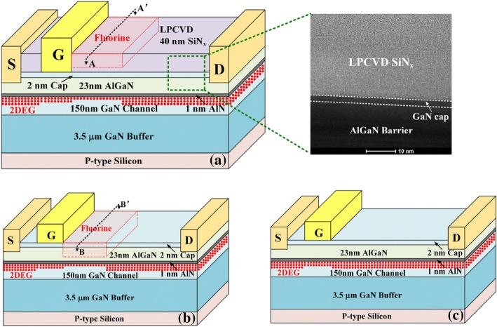
Figure 1 is the three-dimensional schematic of FPL HEMT, FBL HEMT, and Conv. HEMT, respectively. All devices feature a gate length LG of 2.5 μm, a gate-source distance LGS of 1.5 μm, and a gate-drain distance LGD of 10 μm. The epitaxial AlGaN/GaN heterostructure used for fabricating the FPL HEMT was grown on 6-in (111) silicon substrate by metal organic chemical vapor deposition (MOCVD). The epitaxial layers consist of a 2-nm GaN cap, 23-nm Al0.25Ga0.75N barrier, 1-nm AlN interlayer, 150-nm GaN channel, and 3.5-μm GaN buffer. The Hall effect measured density and mobility of the 2DEG were 9.5 × 1012 cm−2 and 1500 cm2/V s, respectively. The proposed FPL HEMT started with mesa isolation which was implemented by a high power Cl2/BCl3-based inductively coupled plasma (ICP) etching. Then, a 40-nm-thick low pressure chemical vapor deposition (LPCVD) SiNx layer was deposited at 780 °C/300 mTorr with a NH3 flow of 280 sccm and a SiH2Cl2 flow of 70 sccm, yielding a deposition rate of 3.7 nm/min. The refractive index is measured by ellipsometer as 1.978, and the N/Si ratio of SiNx is 1.31 [25]. The crystallinity of LPCVD SiNx is amorphous, which is confirmed by high-resolution transmission electron microscope (HR-TEM) micrograph (see the inset of Fig. 1a). After opening the source and drain contact windows by SF6 plasma dry etching, the Ti/Al/Ni/Au (20/150/45/55 nm) ohmic contact was deposited and annealed at 890 °C for 30 s in N2 ambient. The contact resistance of 1 Ω mm and sheet resistance of 400 Ω/square were extracted by the linear transmission line method. Next, the gate metal electrode is formed by Ni/Au (50 nm/150 nm) deposition and lift-off process. Then, the fluorine ion implantation window (Length of window = 3 μm) is formed by AZ5214 photoresist, and fluorine ions were implanted by SEN NV-GSD-HE ion implanter at an energy of 10 keV at a dose of 1 × 1012 cm−2. Finally, the samples were annealed at 400 °C for 15 min in N2 ambient to complete the transistor fabrication flow [26].
Fig. 1.
Three-dimensional schematic of a FPL HEMT (inset: HR-TEM micrograph of LPCVD SiNx), b FBL HEMT, and c Conv. HEMT
Results and Discussion
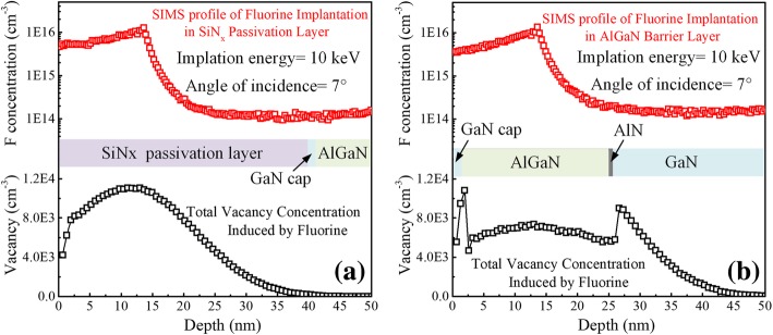
Figure 2 shows the measured secondary ion mass spectroscopy (SIMS) profile of fluorine ion concentration and simulated vacancy concentration by TRIM along the cut lines: (a) A-A′ of FPL HEMT and (b) B-B′ of FBL HEMT, respectively. At the same energy and dose of fluorine ion implantation, the measured peak position from the surface and maximum concentration of the fluorine profile is almost the same for the two structures. In the case of the fluorine ion implantation in the thin AlGaN barrier layer, the vacancies induced by fluorine extend to the 2DEG channel region. The distribution of vacancy concentration is discontinuous at each interface because the bond energy of every material is different [27]. However, in the case of the fluorine ion implantation in the thick SiNx passivation layer, the vacancy distribution is located within the SiNx passivation layer and far from the 2DEG channel. The vacancies induced by ion implantation would trap the 2DEG channel, and 2DEG could be easily trapped if the vacancy distribution is near to the 2DEG [28]. In conclusion, fluorine ion implantation in the thick SiNx passivation layer could significantly reduce the influence of ion implantation on the 2DEG channel and suppress the static and dynamic characteristic degradation effectively.
Fig. 2.
Measured SIMS profile of fluorine ion concentration and simulated vacancy concentration by TRIM along the cut lines. a A-A′. b B-B′
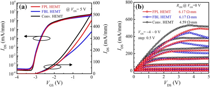
Figure 3 illuminates the measured I-V transfer characteristics and direct current (DC) output characteristics. Compared with the Conv. HEMT, both the FPL HEMT and FBL HEMT show a decrease in IDS and an increase in static ON-resistance (RON), because the fluorine ions cause the assisted depletion of the 2DEG in the drift region and thus decrease the 2DEG density [29]. In addition, the ion implantation also decreases the 2DEG mobility. The Hall effect measured 2DEG mobilities of the FPL and FBL HEMTs are 228 cm2/V s and 203 cm2/V s after ion implantation, respectively. Owing to the same dose of fluorine ions, the output characteristics and RON of FPL HEMT and FBL HEMT are almost the same at a low drain voltage (e.g., VDS < 3 V). However, when VDS > 3 V, the saturation drain current collapse occurs in the FBL HEMT, because the vacancy profile of fluorine extends to the 2DEG channel region, and the 2DEG could be easily trapped by these deep level vacancies induced by fluorine when drain voltage is large than critical drain voltage (e.g., VDS > 3 V) [30], thereby decreasing the drain current. The vacancy distribution of FPL HEMT is far from the 2DEG channel, thus suppressing the saturation drain current collapse effectively.
Fig. 3.
Measured a I-V transfer characteristics, and b DC output characteristics for three HEMTs
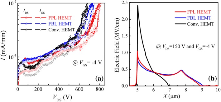
Figure 4 shows the measured I-V characteristics and simulated surface E-field distributions on the blocking state. The BVs of the FPL/FBL/Conv. HEMTs are 803/746/680 V, respectively. The BV is defined as the drain-source voltage at the drain current (IDS) of 1 μA/mm with VGS = − 4 V. The fluorine ions between the gate and drain as a termination technique reduce the E-field peak at the gate edge and cause a new E-field peak at the end of ion implantation region, and thus, FPL HEMT and FBL HEMT achieve more uniform surface E-field distribution and higher BV than that of the Conv. HEMT. Compared with FPL HEMT, FBL HEMT has an enhanced electric field modulation effect, because the fluorine ion profile is near to the 2DEG channel. However, for the FBL HEMT, ion implantation would inevitably induce additional damages in AlGaN barrier [31, 32], leading to a continuous gate leakage current path of gate-barrier layer-2DEG; therefore, the BV of FBL HMET is slightly smaller than that of the FPL HEMT.
Fig. 4.
a Measured off-state I-V characteristics with a gate voltage of−4 V, keeping the substrate floated. b Simulated surface E-field distributions at VDS = 150 V
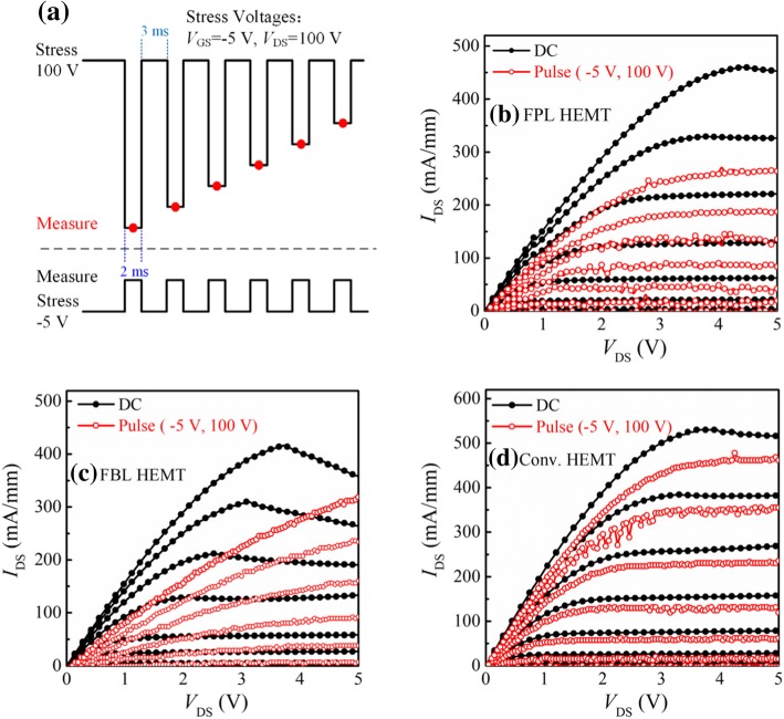
Pulsed IDS-VDS measurements [33] under slow switching were performed to characterize the behavior of dynamic ON-resistance (RON, D) of the fabricated AlGaN/GaN HEMTs. Figure 5a is the schematic depicting the application of stress voltage during the pulsed IDS-VDS measurements. In pulsed I-V measurements, the gate and drain electrodes of the GaN HEMTs were subjected to short voltage pulses before each I-V measurement to ensure that the devices were in the off-state. The pulse width is 3 ms and the period is 5 ms. Figure 5 b–d show the comparison of the pulsed output characteristics of the devices under (VGS0, VDS0) of (0 V, 0 V) and (0 V, 100 V). It can be seen that there is a slightest degradation (12.3%) of dynamic ON-resistance for the Conv. HEMT, owing to the absence of fluorine ion implantation process. In comparison with FBL HEMT, FPL HEMT has a low degradation of dynamic ON-resistance. Owing to the passivation layer, the vacancy distribution is far away from the 2DEG channel and is located within the passivation layer, which suppresses the charge trapping in the FPL HEMT. Figure 6 summarizes the ratio values of RON, D/RON for the three HEMTs under (VGS0, VDS0) from (0 V, 0 V) and (0 V, 100 V) at a step of 20 V. For the FBL HEMT, the measured RON, D is already increased by 98% of the static one at (VGS0, VDS0) of (0 V, 0 V) and (0 V, 100 V), while the RON, D of the FPL HEMT is increased by only 23% at a high drain quiescent bias of 100 V.
Fig. 5.
a Schematic depicting application of stress voltage during the pulsed IDS-VDS measurements. Pulsed IDS-VDS characteristics of the fabricated AlGaN/GaN HEMTs with b FPL HEMT, c FBL HEMT, and d Conv. HEMT (VGS = − 4~0 V; step: 0.5 V)
Fig. 6.
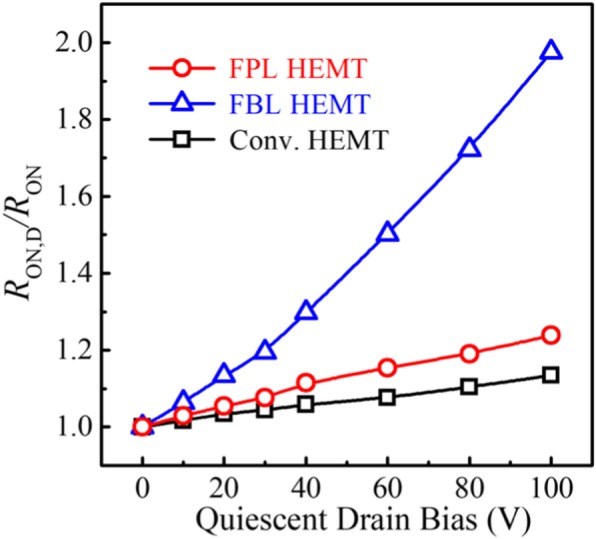
Ratio of RON, D/RON for the fabricated HEMTs at different quiescent drain bias points. The pulse width and period are 3 ms and 5 ms, respectively
Conclusions
In conclusion, we proposed a novel AlGaN/GaN HEMT with a high breakdown voltage and low dynamic ON-resistance. It features fluorine ion implantation in the thick SiNx passivation layer. Fluorine ion implantation in passivation layer could effectively suppress electrical characteristic degradation. The dynamic ON-resistance is only 1.23 times as larger as the static ON-resistance after off-state VDS stress of 100 V, while it is 1.98 times for the FBL HEMT. In addition, the fluorine ions in the passivation layer also modulate the E-filed distribution and spread the depletion region; thus, the BV of the proposed HEMT increases to 803 V from 680 V of conventional AlGaN/GaN HEMT.
Acknowledgements
Not applicable
Abbreviations
- 2DEG
Two-dimensional electron gas
- HEMT
High electron mobility transistor
- ICP
Inductively coupled plasma
- LPCVD
Low pressure chemical vapor deposition
- MOCVD
Metal organic chemical vapor deposition
- SIMS
Secondary ion mass spectroscopy
- TEM
Transmission electron microscope
Authors’ Contributions
CY conceived and performed the experiments and data analysis. XRL supervised this work. All authors discussed the results and contributed to the final manuscript. All authors read and approved the final manuscript.
Funding
This work was supported by the National Natural Science Foundations of China under Grant 51677021 and 61874149.
Availability of Data and Materials
All data generated or analyzed during this study are included in this published article.
Competing Interests
The authors declare that they have no competing interests.
Footnotes
Publisher’s Note
Springer Nature remains neutral with regard to jurisdictional claims in published maps and institutional affiliations.
Contributor Information
Chao Yang, Email: yangchaouestc@gmail.com.
Xiaorong Luo, Email: xrluo@uestc.edu.cn.
Tao Sun, Email: goblinnoon@outlook.com.
Anbang Zhang, Email: anbangzhang@outlook.com.
Dongfa Ouyang, Email: ouyangdongfa@outlook.com.
Siyu Deng, Email: dengsiyuuestc@163.com.
Jie Wei, Email: weijieuestc@gmail.com.
Bo Zhang, Email: zhangbo@uestc.edu.cn.
References
- 1.Mishra UK, Parikh P, Wu YF. AlGaN/GaN HEMTs—an overview of device operations and applications. Proc IEEE. 2002;90:1022–1031. doi: 10.1109/JPROC.2002.1021567. [DOI] [Google Scholar]
- 2.Medina H, Li JG, Su TY, Lan YW, Lee SH, Chen CW, Chen YZ, Manikandan A, Tsai SH, Navabi A, Zhu X, Shih YC, Lin WS, Yang JH, Thomas S, Wu BW, Shen CH, Shieh JM, Lin HN, Javey A, Wang K, Chueh YL. Wafer-scale growth of WSe2 monolayers toward phase-engineered hybrid WOx/WSe2 films with sub-ppb NOx gas sensing by a low-temperature plasma-assisted selenization process. Chem Mater. 2017;29:1587–1598. doi: 10.1021/acs.chemmater.6b04467. [DOI] [Google Scholar]
- 3.Yang Wei, Chen Jiaxin, Zhang Yong, Zhang Yujia, He Jr‐Hau, Fang Xiaosheng. Silicon‐Compatible Photodetectors: Trends to Monolithically Integrate Photosensors with Chip Technology. Advanced Functional Materials. 2019;29(18):1808182. doi: 10.1002/adfm.201808182. [DOI] [Google Scholar]
- 4.Wang Y, Chen Z, Lei T, Ai Y, Peng Z, Yan X, Li H, Zhang J, Wang ZM, Chueh YL. Hollow NiCo2S4 nanospheres hybridized with 3D hierarchical porous rGO/Fe2O3 composites toward high-performance energy storage device. Adv Energy Mater. 2018;8:1703453. doi: 10.1002/aenm.201703453. [DOI] [Google Scholar]
- 5.Gao W, Xia Z, Cao F, Ho JC, Jiang Z, Qu Y. Comprehensive understanding of the spatial configurations of CeO2 in NiO for the electrocatalytic oxygen evolution reaction: embedded or surface-loaded. Adv Funct Mater. 2018;28:1706056. doi: 10.1002/adfm.201706056. [DOI] [Google Scholar]
- 6.Retamal J, Ho CH, Tsai KT, Ke JJ, He JH. Self-organized Al nanotip electrodes for achieving ultralow-power and error-free memory. Trans Electron Devices, IEEE. 2019;66:938–943. doi: 10.1109/TED.2018.2888873. [DOI] [Google Scholar]
- 7.Song L, Luo L, Li X, Liu D, Han N, Liu L, Qin Y, Ho JC, Wang F. Modulating electrical performances of In2O3 nanofiber channel thin film transistors via Sr doping. Adv Electronic Mater. 2019;5:1800707. doi: 10.1002/aelm.201800707. [DOI] [Google Scholar]
- 8.Wang Z, Jiang T, Xu L. Toward the blue energy dream by triboelectric nanogenerator networks. Nano Energy. 2017;39:9–23. doi: 10.1016/j.nanoen.2017.06.035. [DOI] [Google Scholar]
- 9.Chow TP, Tyagi R. Wide bandgap compound semiconductors for superior high-voltage unipolar power devices. Trans Electron Devices, IEEE. 1994;41:1481–1483. doi: 10.1109/16.297751. [DOI] [Google Scholar]
- 10.Ishida M, Ueda T, Tanaka T, Ueda D. GaN on Si technologies for power switching devices. Trans Electron Devices, IEEE. 2013;60:3053–3059. doi: 10.1109/TED.2013.2268577. [DOI] [Google Scholar]
- 11.Park PS, Nath DN, Krishnamoorthy S, Rajan S. Electron gas dimensionality engineering in AlGaN/GaN high electron mobility transistors using polarization. Appl Phys Lett. 2012;100:063507. doi: 10.1063/1.3685483. [DOI] [Google Scholar]
- 12.Huang X, Liu Z, Li Q, Lee FC. Evaluation and application of 600 V GaN HEMT in cascode structure. Trans Power Electron, IEEE. 2014;29:2453–2461. doi: 10.1109/TPEL.2013.2276127. [DOI] [Google Scholar]
- 13.Liao WC, Chen YL, Chen ZX, Chyi JI, Hsin YM. Gate leakage current induced trapping in AlGaN/GaN Schottky-gate HFETs and MISHFETs. Nanoscale Res Lett. 2014;9:474. doi: 10.1186/1556-276X-9-474. [DOI] [PMC free article] [PubMed] [Google Scholar]
- 14.Tan S, Deng X, Zhang B, Zhang J. Thermal stability of F ion-implant isolated AlGaN/GaN heterostructures. Sci China Phys, Mech Astron. 2018;61:127311. doi: 10.1007/s11433-018-9312-7. [DOI] [Google Scholar]
- 15.Dora Y, Chakraborty A, McCarthy L, Keller S, DenBaars SP, Mishra UK. High breakdown voltage achieved on AlGaN/GaN HEMTs with integrated slant field plates. Electron Device Lett, IEEE. 2006;27:713–715. doi: 10.1109/LED.2006.881020. [DOI] [Google Scholar]
- 16.Lee Y, Yao Y, Huang C, Lin T, Cheng L, Liu C, Wang M, Hwang J. High breakdown voltage in AlGaN/GaN HEMTs using AlGaN/GaN/AlGaN quantum-well electron-blocking layers. Nanoscale Res Lett. 2014;9:433. doi: 10.1186/1556-276X-9-433. [DOI] [PMC free article] [PubMed] [Google Scholar]
- 17.Song B, Sensale-Rodriguez B, Wang R, Guo J, Hu Z, Yue Y, Faria F, Schuette M, Ketterson A, Beam E, Saunier P, Gao X, Guo S, Fay P, Jena D, Xing H. Effect of fringing capacitances on the RF performance of GaN HEMTs with T-gates. Trans Electron Devices, IEEE. 2014;61:747–754. doi: 10.1109/TED.2014.2299810. [DOI] [Google Scholar]
- 18.Ando Y, Okamoto Y, Miyamoto H, Nakayama T, Inoue T, Kuzuhara M. 10-W/mm AlGaN-GaN HFET with a field modulating plate. Electron Device Lett, IEEE. 2003;24:289–291. doi: 10.1109/LED.2003.812532. [DOI] [Google Scholar]
- 19.Wu Y, Moore M, Wisleder T, Chavarkar PM, Mishra UK, Parikh P. Proc. Int. Electron Device Meeting (IEDM), San Francisco, CA, IEEE. 2004. High-gain microwave GaN HEMTs with source-terminated field-plates; pp. 1078–1079. [Google Scholar]
- 20.Song D, Liu J, Cheng Z, Tang WCW, Lau KM, Chen KJ. Normally off AlGaN/GaN low-density drain HEMT (LDD-HEMT) with enhanced breakdown voltage and reduced current collapse. Electron Device Lett, IEEE. 2007;28:189–191. doi: 10.1109/LED.2007.891281. [DOI] [Google Scholar]
- 21.Wang M, Chen KJ. Improvement of the off-state breakdown voltage with fluorine ion implantation in AlGaN/GaN HEMTs. Trans Electron Devices, IEEE. 2011;58:460–464. doi: 10.1109/TED.2010.2091958. [DOI] [Google Scholar]
- 22.Kim YS, Lim J, Seok OG, Han MK. Proc. 23rd international symposium on power semiconductor dev and IC's (ISPSD), San Diego, CA, IEEE. 2011. High breakdown voltage AlGaN/GaN HEMT by employing selective fluoride plasma treatment; pp. 203–206. [Google Scholar]
- 23.Yang C, Luo X, Zhang A, Deng S, Ouyang D, Peng F, Wei J, Zhang B, Li Z. AlGaN/GaN MIS-HEMT with AlN interface protection layer and trench termination structure. Trans Electron Devices, IEEE. 2018;65:5203–5207. doi: 10.1109/TED.2018.2868104. [DOI] [Google Scholar]
- 24.Kim M, Choi YH, Lim J, Kim YS, Seok O, Mk H. Proc. international conference on compound semiconductor manufacturing technology (CS MANTECH), Portland, Oregon. 2010. High breakdown voltage AlGaN/GaN HEMTs employing recessed gate edge structure; pp. 237–240. [Google Scholar]
- 25.Makino T. Composition and structure control by source gas ratio in LPCVD SiNx. J Electrochem Soc. 1983;130:450–455. doi: 10.1149/1.2119729. [DOI] [Google Scholar]
- 26.Zhang Z, Fu K, Deng X, Zhang X, Fan Y, Sun S, Song L, Xing Z, Huang W, Yu G, Cai Y, Zhang B. Normally off AlGaN/GaN MIS-high-electron mobility transistors fabricated by using low pressure chemical vapor deposition Si3N4 gate dielectric and standard fluorine ion implantation. Electron Device Lett, IEEE. 2015;36:1128–1131. doi: 10.1109/LED.2015.2483760. [DOI] [Google Scholar]
- 27.Costales A, Blanco M, Pendás M, Kandalam A, Pandey R. Chemical bonding in group III nitrides. J Am Chem Soc. 2002;124:4116–4123. doi: 10.1021/ja017380o. [DOI] [PubMed] [Google Scholar]
- 28.Meneghini M, Ronchi N, Stocco A, Meneghesso G, Mishra UK, Pei Y, Zanoni E. Investigation of trapping and hot-electron effects in GaN HEMTs by means of a combined electrooptical method. Trans Electron Devices, IEEE. 2011;58:2996–3003. doi: 10.1109/TED.2011.2160547. [DOI] [Google Scholar]
- 29.Yang C, Xiong J, Wei J, Wu J, Zhang B, Luo X (2015) High performance enhancement-mode AlGaN/GaN MIS HEMT with selective fluorine treatment. Adv Condens Matter Phys 2015:267680
- 30.Khan MA, Shur MS, Chen QC, Kuznia JN. Current/voltage characteristic collapse in AlGaN/GaN heterostructure insulated gate field effect transistors at high drain bias. Electronics Lett. 1994;30:2175–2176. doi: 10.1049/el:19941461. [DOI] [Google Scholar]
- 31.Schustereder W, Fuchs D, Humbel O, Brunner B, Pölzl M. Ion implantation challenges for power devices. AIP Conf Proc. 2012;1496:16–21. doi: 10.1063/1.4766479. [DOI] [Google Scholar]
- 32.Xiong J, Yang C, Wei J, Wu J, Zhang B, Luo X. Novel high voltage RESURF AlGaN/GaN HEMT with charged buffer layer. Sci China Inf Sci. 2016;59:042410. doi: 10.1007/s11432-015-5454-z. [DOI] [Google Scholar]
- 33.Omika K, Tateno Y, Kouchi T, Komatani T, Yaegassi S, Yui K, Nakata K, Nagamura N, Kotsugi M, Horiba K, Oshima M, Suemitsu M, Fukidome H. Operation mechanism of GaN-based transistors elucidated by element-specific x-ray nanospectroscopy. Sci Rep. 2018;8:13268. doi: 10.1038/s41598-018-31485-4. [DOI] [PMC free article] [PubMed] [Google Scholar]
Associated Data
This section collects any data citations, data availability statements, or supplementary materials included in this article.
Data Availability Statement
All data generated or analyzed during this study are included in this published article.


