Abstract
By adopting the first-principle methods based on the density functional theory, we studied the structural, electronic, and magnetic properties of defected monolayer WSe2 with vacancies and the influences of external strain on the defected configurations. Our calculations show that the two W atom vacancies (VW2) and one W atom and its nearby three pairs of Se atom vacancies (VWSe6) both induce magnetism into monolayer WSe2 with magnetic moments of 2 and 6 μB, respectively. The magnetic moments are mainly contributed by the atoms around the vacancies. Particularly, monolayer WSe2 with VW2 is half-metallic. Additionally, one Se and one W atom vacancies (VSe, VW), two Se atom vacancies (VSe-Se), and one W atom and the nearby three Se atoms on the same layer vacancy (VWSe3)-doped monolayer WSe2 remain as non-magnetic semiconducting. But the impure electronic states attributed from the W d and Se p orbitals around the vacancies locate around the Fermi level and narrow down the energy gaps. Meanwhile, our calculations indicate that the tensile strain of 0~7% not only manipulates the electronic properties of defected monolayer WSe2 with vacancies by narrowing down their energy gaps, but also controls the magnetic moments of VW-, VW2-, and VWSe6-doped monolayer WSe2.
Keywords: Monolayer WSe2, Vacancy, External strain, Electronic properties, Magnetic properties, First-principle calculations
Introduction
Unlike gapless graphene [1, 2], semiconducting transition metal dichalcogenide (TMD) monolayers with a band gap of 1~2 eV [3–6] have superior advantages in the fields of catalyst, electronics, and optoelectronics because of their unique chemical, optical, and electronic properties [3–9]. Particularly, monolayer WSe2 is semiconducting with a direct band gap of ~ 1.6 eV [4, 10–12]. Additionally, its carrier mobility is around 250 cm2/V, and the on/off ratio is higher than 106 at room temperature [13]. More importantly, monolayer WSe2 is the first TMD showing p-type conducting behavior with high work function metal (Pd) being the contacts [13]. Because of these novel properties, monolayer WSe2 has been widely studied as the promising candidate in the future electronics and optoelectronics [4, 6, 13–16]. However, monolayer WSe2 is non-magnetic which limits its application in many other fields related with magnetism.
Based on the previous studies [17–25], structural defects significantly influence the mechanical, electronic, and magnetic properties. For example, point defect and vacancy defect introduce magnetism into graphene [19, 20], MoS2 monolayer, and BaTiO3(001) thin film [21–23], respectively. Wu et al. studied the effects of defects on the device transmission performance in monolayer WSe2 tunneling field-effect transistors (TFSTs) by performing the ab initio calculation, which indicates that defects can be well designed to obtain high-performance TFETs [25]. Meanwhile, structural defects were found in the as-grown 2D materials due to the imperfection of the growth process [19, 20, 26–28]. For example, intrinsic structural defects, such as point defects, are noticeable in the as-grown monolayer WSe2 [26].
Indeed, structural engineering methods including irradiation by high energy particles of electron beam [29], ion beam [30] and high energy laser, and chemical etching [31, 32] are the effective techniques to induce defects in the 2D materials and have been used to modify the atomic structures. Therefore, it is not only significant but also realistic to study the influence of structural defects such as vacancies on the properties of monolayer WSe2, which may offer us the new feature. Additionally, the 2D materials can withstand large strains before rupture and even be stretched beyond the inherent limit of 10% owing to their strong plastic deformation ability as demonstrated on monolayer MoS2 [33, 34]. Thus, strain engineering has been widely used to tune the properties of 2D materials and enhance the relevant performance in the related applications [11, 17, 33–39]. According to Yang et al.’s study, nanoscale local strain modifies the optical band gap and changes the electronic and magnetic properties of monolayer ReSe2 [38]. Particularly, it was reported that the non-magnetic WS2 monolayer becomes ferromagnetic under the applied biaxial strain, and the highest magnetic moment reaches 4.85 μB [39].
In this work, we systematically investigated the effects of vacancy defects and tensile strain on the electronic properties of monolayer WSe2. We calculated several vacancy defects of single atom vacancy, double atom vacancy, and big vacancies of four and seven atoms. We found that all the vacancy defects change the electronic properties of monolayer WSe2, while only the VW2 and VWSe6 vacancies introduce the magnetism of 2 and 6 μB, respectively. Additionally, monolayer WSe2 with VW vacancy converts into magnetic from non-magnetic under the external tensile strain. More importantly, the external biaxial strain effectively modulates not only the energy gaps but also the magnetic moments of VW-, VW2-, and VWSe6-doped monolayer WSe2. Our calculations suggest defected monolayer WSe2 with vacancies as potential monolayer magnetic semiconductors.
Computational Methods
All the calculations in the present study were performed by adopting the Vienna Ab initio Simulation Package (VASP) based on density functional theory (DFT) [40, 41]. The Perdew–Burke–Ernzerhof (PBE) method was used to calculate the electronic exchange interaction [42]. The ion–electron and electron–electron interactions were calculated by the projector augmented wave (PAW) method and the plane wave basis set [43, 44]. The cutoff energy for the plane wave basis set was set to 300 eV, and the first Brillouin zone was sampled by the 3 × 3× 1 k-mesh based on the Monkhorst–Pack method [45]. A vacuum space of 15 Å was added along the vertical direction above the monolayer to remove the interactions between the adjacent images in the periodic slab model. Structure relaxations have been carried out until all the forces on each ion are less than 0.02 eV/Å, and the convergence criteria for the total energy were set as 10−4 eV. The biaxial tensile strain was imposed on the vacancy defect–doped monolayer WSe2, which was calculated by ε = (c − c0)/c0 × 100%, where c and c0 are the lattice parameters of the strained and free monolayer WSe2, respectively.
Results and Discussion
Atomic Structure and Electronic Properties of Monolayer WSe2
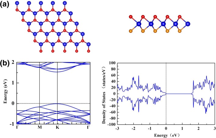
The most stable crystal structure of monolayer WSe2, denoted as 1H-WSe2, is shown in Fig. 1a, which shows the sandwiched layer of Se-WSe. In 1H-WSe2, W atoms and Se atoms occupy the sublattices of hexagonal sheet, and the Se atoms on the lower layer are directly underneath those Se atoms on the upper layer. Our calculated W-W bond length is 3.31 Å and the W-Se bond length is 2.54 Å, agreeing well with previous results [10, 11]. As shown in Fig. 1b, the calculated electronic band structure and density of states (DOS) for 1H-WSe2 indicate that 1H-WSe2 is non-magnetic semiconducting with a direct band gap of 1.54 eV. Our calculated result agrees well with the previous result of 1.55 eV [12]. To get a more accurate band gap, we adopted the Heyd–Scuseria–Ernzerh (HSE06) [46] method to calculate the electronic band structure. The energy gap of 1H-WSe2 calculated by HSE06 method is 2.0 eV.
Fig. 1.
a Top and side views for the atomic structure of monolayer WSe2. b The electronic band structure and density of states (DOS) of monolayer WSe2. The blue, red, and tangerine balls represent Wand Se atoms on the top and bottom layer, respectively. Fermi level is set as 0 eV
The Magnetic and Electronic Properties of Defected Monolayer WSe2 with Vacancy
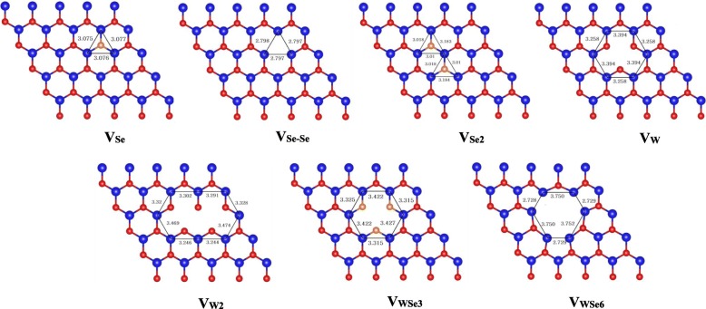
We considered seven vacancy defect configurations for monolayer WSe2 in the present study. They are the single atom vacancies including one Se atom vacancy (VSe), one W atom vacancy (VW), and two atom vacancies of VSe-Se, VSe2, and VW2. The two Se atom vacancy VSe-Se means the two Se atoms which are just beneath or above each other are removed, while the VSe2/VW2 vacancy means that the two adjacent Se/W atoms are removed. We also considered the big vacancies of VWSe3 and VWSe6. VWSe3 denotes the vacancy of one W atom and the nearby three Se atoms on the same layer, and VWSe6 presents the vacancy of one W atom and the nearby three pairs of Se atoms. The optimized structures of monolayer WSe2 with vacancies of VSe, VSe-Se, VSe2, VW, VW2, VWSe3, and VWSe6 are shown in the insets of Fig. 2. As we can see, the 5 × 5 × 1 supercell was used for the present study of the defected monolayer WSe2.
Fig. 2.
The optimized atomic structures of monolayer WSe2 with VSe, VSe-Se, VSe2, VW, VW2, VWSe3, and VWSe6 vacancies. The blue, red, and tangerine balls represent W and Se atoms on the top and bottom layer, respectively
Table 1 summarizes the results for the defected monolayer WSe2 with vacancies of VSe, VSe-Se, VSe2, VW, VW2, VWSe3, and VWSe6. We can see that the W-W distances around the vacancies of VSe, VSe-Se, and VSe2 decrease respectively by 0.23, 0.52, and 0.24 Å compared with the original W-W distance in monolayer WSe2, which means that the W atoms around the Se atoms vacancies get close to each other. Additionally, the W-W distances around the vacancies of VW, VW2, and VWSe3 slightly increase by 0.02, 0.01, and 0.06 Å. And those W-W distances around the single atom vacancies (VSe /VW) are almost equal to the counterpart around the two atoms vacancies (VSe2/VW2). For the bigger vacancy VWSe6-doped monolayer WSe2, the W-W distances between the neighboring W atoms at the corners of the vacancy reduce by 0.58 Å, but the W-W distances at the edges of the vacancy increase by 0.44 Å. The formation energies of the seven vacancy geometries are calculated via:
Table 1.
The calculation results for monolayer WSe2 with VSe, VSe-Se, VSe2, VW, VW2, VWSe3, and VWSe6 vacancies
| 1H-WSe2 | VSe | VSe ‐ Se | VSe2 | VW | VW2 | VWSe3 | VWSe6 | |
|---|---|---|---|---|---|---|---|---|
| dW ‐ W (Å) | 3.31 | 3.08 | 2.79 | 3.07 | 3.33 | 3.32 | 3.37 | 2.73a/3.75b |
| Egap (eV) | 1.54 | 1.18 | 1.15 | 1.02 | 0.18 | 0.19 c | 0.76 | 0.1 |
| Mtot ( μB) | 0 | 0 | 0 | 0 | 0 | 2 | 0 | 6 |
| Eform (eV) | – | 2.66 | 4.7 | 5.39 | 5.35 | 9.43 | 8.85 | 16.55 |
dW ‐ W the averaged W-W distances around the vacancy; Egap and Mtot the energy gaps and total magnetic moments, respectively; Eform the formation energy. The calculation results for the perfect 1H-WSe2 are also listed.
a, bThe W-W distance between the neighboring W atoms at the corners and at the edges around the VWSe6, respectively
cThe energy gap for the half-metal
and are the total energies of the 5 × 5 × 1 supercell of monolayer WSe2 with and without vacancy defect, and ui and ni (i = Se, W) are the chemical potential and number of the removed i atom. As listed in Table 1, our calculated formation energies for the seven vacancies indicate that VSe, the single Se atom vacancy, should be frequently observed on WSe2 monolayer, consistent with the previous result of monolayer MoS2 [17, 21]. For the two Se atom vacancies of VSe-Se and VSe2, the formation energy of VSe2 is a little higher than that of VSe-Se, indicating that VSe-Se is energetically preferable than VSe2. Hence, in the following study, only VSe-Se is studied as the two Se atom vacancies. Additionally, the formation energies for the big size vacancies are higher, which may be generated via certain kind of structural engineering techniques [29–31].
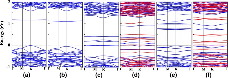
We then studied the electronic properties of the defected monolayer WSe2 with vacancies of VSe, VSe-Se, VW, VW2, VWSe3, and VWSe6. Figure 3 shows the electronic band structures of the six vacancy-doped monolayer WSe2. As shown in Fig. 3a, VSe-doped monolayer WSe2 remains to be semiconducting, but there are obviously extra electronic states generated from the vacancy defect locating in the gap region. Consequently, the energy gap of VSe-doped monolayer WSe2 reduces to 1.18 eV compared with that of monolayer WSe2. The electronic band structure of VSe-Se-doped monolayer WSe2 is similar with that of VSe-doped monolayer WSe2, and their energy gaps are close. VW- and VWSe3-doped monolayer WSe2 shown in Fig. 3c and e also maintains the semiconducting feature but with much smaller energy gaps of 0.18 and 0.76 eV, respectively. Different from the above vacancy defects, the majority and the minority spin channels are distributed asymmetrically for the VW2- and VWSe6-doped monolayer WSe2 as shown, in Fig. 3d and f. For the VW2-doped monolayer WSe2, the majority spin channels cross the Fermi level, while the minority spin channels maintain semiconducting with an energy gap of 0.19 eV, and its magnetic moment is 2.0 μB, while the VWSe6-doped monolayer WSe2 is magnetic semiconducting with a magnetic moment of 6.0 μB.
Fig. 3.
The electronic band structures of monolayer WSe2 with a VSe, b VSe-Se, c VW, d VW2, e VWSe3, and f VWSe6 vacancies. Blue and red lines represent the majority and minority spin channels, respectively. Fermi level is set as 0 eV
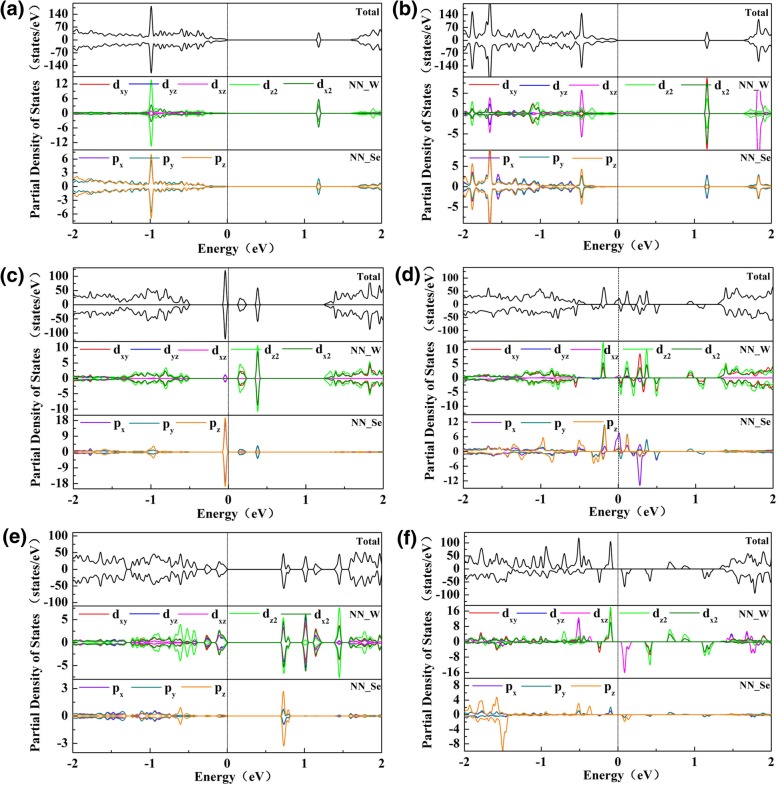
We also calculated the partial density of states (PDOS) for the six vacancy-doped monolayer WSe2 to further study their electronic properties. Figure 4 shows that the impure electronic states of VSe- and VSe-Se-doped monolayer WSe2 are mostly located in conduction band region, and they are mainly derived from the d orbital of W atoms near the vacancy, and little from p orbital of Se atoms around the vacancy. Differently, the impure electronic bands of VW- and VWSe3-doped monolayer WSe2 are not only located in the conduction band region, but also being split in the valence band region. For VW vacancy, the conduction bands near the Fermi level mainly come from the d (dxy, dx2and dz2) orbitals of the W atoms around the vacancy, and the valence bands near the Fermi level are mainly from the p orbital of Se atoms around the vacancy. Compared with VW-doped monolayer WSe2, the impure electronic states of VWSe3-doped monolayer WSe2 are further away from the Fermi level. The conduction bands near the Fermi level are derived from both the Se pzorbital and W d orbitals around the vacancy, while the valence bands near the Fermi level are mainly from the W d orbital around the vacancy. Additionally, W d orbital and the neighboring Se p orbital strongly interact, resulting in the hybridized states around the Fermi level. For the half-metallic VW2-doped monolayer WSe2, the conduction band cross of the Fermi level mainly comes from the Se pxorbital, and the valence bands near the Fermi level are mainly derived from the W d (dx2 and dz2) orbital. As for the magnetic semiconducting VWSe6-doped monolayer WSe2, the conduction bands and the valence bands near the Fermi level are both derived from the W d orbital near the vacancy.
Fig. 4.
The partial density of states (PDOS) of monolayer WSe2 with a VSe, b VSe-Se, c VW, d VW2, e VWSe3, and f VWSe6 vacancies. NN_W and NN_Se represent the nearest neighboring W and Se atoms around the vacancy, respectively. Fermi level is set as 0 eV
The Electronic and Magnetic Properties of Monolayer WSe2 with Vacancy Defect Under Tensile Strain
We further studied the electronic and magnetic properties of the vacancy-doped monolayer WSe2 under the biaxial strain since the strain is an effective way to tune the electronic structures and magnetic moments of the 2D materials. We firstly studied the 1H-WSe2 monolayer under the biaxial strain. Our calculation result shows that the biaxial strain ranging from 0 to 7% does not induce any magnetism into monolayer WSe2, similar with monolayer MoS2 [34, 36]. Additionally, monolayer WSe2 still keeps the semiconducting nature with the energy gap decreasing to 0.5 eV at 7% strain, and the W-W bond length increases as the applied tensile strain increases.
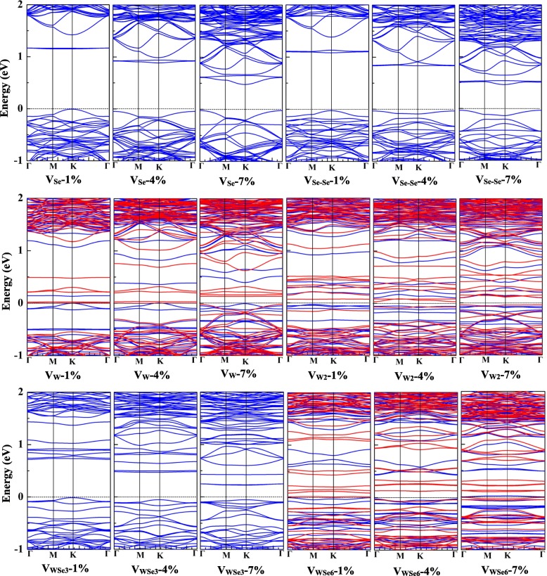
Then, we studied the vacancy-doped monolayer WSe2 under the tensile strain of 0~7%. Figure 5 shows the electronic band structures for VSe-, VSe-Se-, VW-, VW2-, VWSe3-, and VWSe6-doped monolayer WSe2 under the biaxial strain of 1%, 4%, and 7%. Similar with the pristine WSe2 monolayer, VSe-, VSe-Se-, and VWSe3-doped monolayer WSe2 all maintain the semiconducting feature under the biaxial strain of 0~7%, and the conduction band minima are getting closer to the Fermi level as the applied tensile strain increases. For the VW-doped monolayer WSe2 under the biaxial strain larger than 1%, the majority and minority spin channels distribute asymmetrically. Additionally, the VW2- and VWSe6-doped monolayer WSe2 both show magnetic semiconducting feature under the strain of 1~7%. Though the VSe-, VSe-Se-, and VWSe3-doped monolayer WSe2 still keep the semiconducting feature under the biaxial strain of 0~7%, the biaxial strain effectively controls their energy gaps as shown in Fig. 6a. The energy gaps of VSe- and VSe-Se-doped monolayer WSe2 both decrease from 1.1 to 0.5 eV, while the energy gap of VWSe3-doped monolayer WSe2 is relatively smaller, which decreased from 0.76 to 0.3 eV. On the other hand, the energy gaps of VW-, VW2-, and VWSe6-doped monolayer WSe2 are less than 0.2 eV under the biaxial strain of 0~7%.
Fig. 5.
The electronic band structures of monolayer WSe2 with VSe, VSe-Se, VW, VW2, VWSe3, and VWSe6 vacancies under 1%, 4%, and 7% tensile strain. Blue and red lines represent the majority and minority spin channels, respectively. Fermi level is set as 0 eV
Fig. 6.
a The energy gaps of monolayer WSe2 with VSe, VSe-Se, and VWSe3 vacancies. b The magnetic moments of monolayer WSe2 with VW, VW2, and VWSe6 vacancies under the tensile strain of 0~7%.
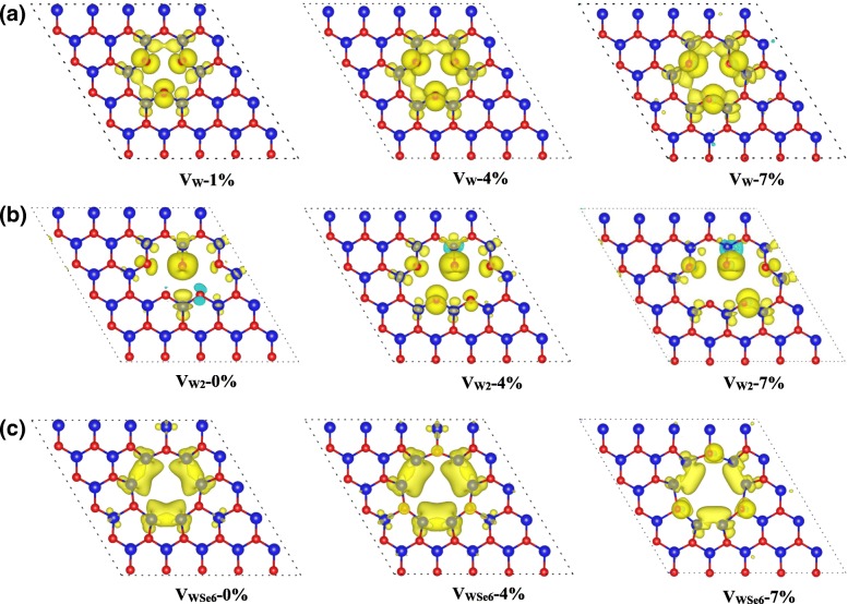
Under the biaxial strain of 0~7%, the VSe-, VSe-Se-, and VWSe3-doped monolayer WSe2 remain to be non-magnetic as shown in Fig. 5. In contrast, the non-magnetic VW-doped monolayer WSe2 become magnetic with the magnetic moment of 4 μB under the biaxial strain larger than 1%. The spin-resolved charge density shown in Fig. 7a indicates that the magnetic moment mainly arises from the W and Se atoms around the vacancies. As shown in Fig. 7b, the magnetic moment of VW2-doped monolayer WSe2 mainly comes from the Se atoms near the vacancy and little from the W atoms around the vacancy. When the applied strain is larger than 1%, more Se atoms are spin-polarized, resulting in the larger magnetic moment of 4 μB. For VWSe6 vacancy defect, we can see that its magnetic moment remains to be 6 μB under the strain of 0~6% and then decreases to 4 μB at the strain of 7% as shown in Fig. 6b. Figure 7c demonstrates that its magnetic moments mainly arise from the six W atoms around VWSe6. When the applied strain increases to 7%, the nearby Se atoms around the vacancy are more spin-polarized, but the local magnetic moments on the W atoms decrease. Correspondingly, the total magnetic moment of VWSe6-doped WSe2 decreases to 4 μB under 7% strain.
Fig. 7.
Spin-resolved charge density of monolayer WSe2 with a VW, b VW2, and c VWSe6 vacancies under the tensile strain of 0~7%. Yellow and cyan isosurfaces represent the positive and negative spin densities, respectively
Conclusion
In summary, we studied several vacancy defects for monolayer WSe2, including the single Se and W atom vacancies (VSe and VW), double Se and W atom vacancies (VSe-Se and VW2), big vacancy of one W atom and the nearby three Se atoms on the same layer (VWSe3), and vacancy of one W atom and the nearby three pairs of Se atoms (VWSe6). The VSe-, VSe-Se-, VW-, and VWSe3-doped monolayer WSe2 all keep the non-magnetic semiconducting feature as the perfect WSe2 monolayer, but with smaller energy gaps due to the impure electronic states locating in the energy gap region, which are attributed from the W d and Se p orbital around the vacancies, while VW2 and VWSe6 vacancies induced magnetism into monolayer WSe2 with magnetic moments of 2 and 6 μB, respectively. Particularly, monolayer WSe2 with VW2 vacancy converts into half-metal from semiconducting. More importantly, our calculation results show that the external biaxial strain effectively tunes the magnetism and electronic properties of monolayer WSe2.
Acknowledgements
Not applicable
Funding
This work was supported by the National key R&D Program of China (2018YFB0703800) and the National Natural Science Foundation of China (NNSFC) (21273172). This work was also supported by the 111 Project (B08040) and the Fundamental Research Funds for the Central Universities (3102015BJ(II)JGZ005, 3102015BJ023) in China.
Availability of Data and Materials
The datasets generated during and/or analyzed during the current study are available from the corresponding author on reasonable request.
Abbreviations
- 2D
Two-dimensional
- CVD
Chemical vapor deposition method
- DFT
The density functional theory
- DOS
The density of states
- HSE06
The Heyd–Scuseria–Ernzerh method
- PAW
The projector augmented wave method
- PBE
The Perdew–Burke–Ernzerhof method
- PDOS
The partial density of states
- TMDs
Transition metal dichalcogenides
- VASP
Vienna Ab initio Simulation Package
Authors’ Contributions
FXZ designed the study, performed the research, and drafted the original manuscript. DXY drafted the revised manuscript. YH and ZFL participated in part of the research. XLF supervise the research and revised the original and revised manuscript. All authors read and approved the final manuscript.
Competing Interests
The authors declare that they have no competing interests.
Publisher’s Note
Springer Nature remains neutral with regard to jurisdictional claims in published maps and institutional affiliations.
Contributor Information
Danxi Yang, Email: yangdanxi@mail.nwpu.edu.cn.
Xiaoli Fan, Email: xlfan@nwpu.edu.cn.
Fengxia Zhang, Email: 2466419810@mail.nwpu.edu.cn.
Yan Hu, Email: sheikha@mail.nwpu.edu.cn.
Zhifen Luo, Email: zhifenluo@mail.nwpu.edu.cn.
References
- 1.JY CAS, Karakaya M, Dandeliya S, Srivastava A, Lin Y, Rao AM, Podila R. Defect-engineered graphene for high-energy- and high-power-density supercapacitor devices. Adv Mater. 2016;28:7185–7192. doi: 10.1002/adma.201602028. [DOI] [PubMed] [Google Scholar]
- 2.Geim AK, Novoselov KS. The rise of graphene. Nat Mater. 2007;6(3):183–191. doi: 10.1038/nmat1849. [DOI] [PubMed] [Google Scholar]
- 3.Fan XL, Wang SY, An YR, Lau WM. Catalytic activity of MS2 monolayer for electrochemical hydrogen evolution. J Phys Chem C. 2016;120:1623–1632. doi: 10.1021/acs.jpcc.5b10709. [DOI] [Google Scholar]
- 4.Choi W, Choudhary N, Han GH, Park J, Akinwande D, Lee YH. Recent development of two-dimensional transition metal dichalcogenies and their applications. Materials Today. 2017;20(3):116–130. doi: 10.1016/j.mattod.2016.10.002. [DOI] [Google Scholar]
- 5.Fan XL, Yang Y, Xiao P, Lau WM. Site-specific catalytic activity in exfoliated MoS2 single-layer polytypes for hydrogen evolution: basal plane and edges. J Mater Chem A. 2014;2:20545–20551. doi: 10.1039/C4TA05257A. [DOI] [Google Scholar]
- 6.Wang QH, Kalantar-Zadeh K, Kis A, Coleman JN, Strano MS. Electronics and optoelectronics of two-dimensional transition metal dichalcogenides. Nature Nanotech. 2012;7(11):699–712. doi: 10.1038/nnano.2012.193. [DOI] [PubMed] [Google Scholar]
- 7.Fiori G, Bonaccorso F, Iannaccone G, Palacios T, Neumaire D, Seabaugh A, Banerjee SK, Colombo L. Electronics based on two-dimensional materials. Nature Nanotech. 2014;9(10):768–779. doi: 10.1038/nnano.2014.207. [DOI] [PubMed] [Google Scholar]
- 8.Jariwala D, Sangwan VK, Lauhon LJ, Marks TJ, Hersam MC. Emerging device applications for semiconducting two-dimensional transition metal dichalcogenides. ACS Nano. 2014;8(2):1102–1120. doi: 10.1021/nn500064s. [DOI] [PubMed] [Google Scholar]
- 9.Yu QM, Shan WZ, Wang HM. Theoretical design of sandwich two-dimensional structures for photocatalysts and nano-optoelectronic. J Mater Sci. 2018;53:8274–8284. doi: 10.1007/s10853-018-2111-0. [DOI] [Google Scholar]
- 10.Ataca C, Şahin H, Ciraci S. Stable, single-layer MX2 transition-metal oxides and dichalcogenides in a honeycomb-like structure. J Phys Chem C. 2012;116:8983–8999. doi: 10.1021/jp212558p. [DOI] [Google Scholar]
- 11.Yun WS, Han SW, Hong SC, Kim IG, Lee JD. Thickness and strain effects on electronic structures of transition metal dichalcogenides: 2H-MX2 semiconductors (M = Mo, W; X = S, Se, Te) Phys Rev B. 2012;85:033305. doi: 10.1103/PhysRevB.85.033305. [DOI] [Google Scholar]
- 12.Zhuang HL, Henning RG. Computational search for single-layer transition-metal dichalcogenide photocatalysts. J Phys Chem C. 2013;117:20440–20445. doi: 10.1021/jp405808a. [DOI] [Google Scholar]
- 13.Fang H, Chuang S, Chang TC, Takei K, Takahashi T, Javey A. High-performance single layered WSe2 p-FETs with chemically doped contacts. Nano Lett. 2012;12(7):3788–3792. doi: 10.1021/nl301702r. [DOI] [PubMed] [Google Scholar]
- 14.Ross JS, Klement P, Jones AM, Ghimire NJ, Yan J, Mandrus DG, Taniguchi T, Watanabe K, Kitamura K, Yao W, Cobden DH, Xu X. Electrically tunable excitonic light-emitting diodes based on monolayer WSe2 p-n junctions. Nature Nanotech. 2014;9(4):268–272. doi: 10.1038/nnano.2014.26. [DOI] [PubMed] [Google Scholar]
- 15.Baugher BWH, Churchill HOH, Yang YF, Jarillo-Herrero P. Optoelectronic devices based on electrically tunable p-n diodes in a monolayer dichalcogenide. Nature Nanotach. 2014;9(4):262–267. doi: 10.1038/nnano.2014.25. [DOI] [PubMed] [Google Scholar]
- 16.Pospischil A, Furchi MM, Mueller T. Solar-energy conversion and light emission in an atomic monolayer P-N diode. Nature Nanotech. 2014;9(4):257–261. doi: 10.1038/nnano.2014.14. [DOI] [PubMed] [Google Scholar]
- 17.Song Hong-Yue, Lü Jing-Tao. Single-site point defects in semimetal WTe2: A density functional theory study. AIP Advances. 2018;8(12):125323. doi: 10.1063/1.5057723. [DOI] [Google Scholar]
- 18.Zhou Wu, Zou Xiaolong, Najmaei Sina, Liu Zheng, Shi Yumeng, Kong Jing, Lou Jun, Ajayan Pulickel M., Yakobson Boris I., Idrobo Juan-Carlos. Intrinsic Structural Defects in Monolayer Molybdenum Disulfide. Nano Letters. 2013;13(6):2615–2622. doi: 10.1021/nl4007479. [DOI] [PubMed] [Google Scholar]
- 19.Nair RR, Sepioni M, Tsai IL, Lehtinen O, Keinonen J, Krasheninnikov AV, Thomson T, Geim AK, Grigorieva IV. Spin-half paramagnetism in graphene induced by point defects. Nature Phys. 2012;8(3):199–202. doi: 10.1038/nphys2183. [DOI] [Google Scholar]
- 20.Yazyev OV. Emergence of magnetism in graphene materials and nanostructures. Rep Prog Phys. 2010;73(5):56501–56516. doi: 10.1088/0034-4885/73/5/056501. [DOI] [Google Scholar]
- 21.Zhou YG, Yang P, Zu HY, Gao F, Zu XT. Electronic structures and magnetic properties of MoS2 nanostructures: atomic defects, nanoholes, nanodots and antidots. Phys Chem Chem Phys. 2013;15(25):10385–10394. doi: 10.1039/c3cp50381j. [DOI] [PubMed] [Google Scholar]
- 22.Cao D, Cai MQ, Hu WY, Yu P, Huang HT. Vacancy-induced magnetism in BaTiO3(001) thin films based on density functional theory. Phys Chem Chem Phys. 2011;13(10):4738–4745. doi: 10.1039/c0cp02424d. [DOI] [PubMed] [Google Scholar]
- 23.Cai MQ, Zhang YJ, Yin Z, Zhang MS. First-principles study of structural and electronic properties of BaTiO3(001) oxygen-vacancy surfaces. Phys Rev B. 2005;72(7):075406. doi: 10.1103/PhysRevB.72.075406. [DOI] [PubMed] [Google Scholar]
- 24.Tongay S, Suh J, Ataca C, Fan W, Luce A, Kang JS, Liu J, Ko C, Raghunathanan R, Zhou J, Ogletree F, Li JB, Grossman JC, Wu JQ. Defects activated photoluminescence in two-dimensional semiconductors: interplay between bound, charged, and free excitons. Sci Rep. 2013;3(6151):2657. doi: 10.1038/srep02657. [DOI] [PMC free article] [PubMed] [Google Scholar]
- 25.Wu JX, Ma XL, Chen JZ, Jiang XW. Defects coupling impacts on mono-layer WSe2 tunneling field-effect transistor. Appl Phys Express. 2019;12:034001. doi: 10.7567/1882-0786/ab00ea. [DOI] [Google Scholar]
- 26.Zhao SD, Tao L, Miao P, Wang XJ, Liu ZG, Wang Y, Li BS, Sui Y, Wang Y. Strong room-temperature emission from defect states in CVD-grown WSe2 nanosheets. Nano Research. 2018;11(7):3922–3930. doi: 10.1007/s12274-018-1970-7. [DOI] [Google Scholar]
- 27.Zheng HL, Yang BS, Wang DD, Han RL, Du XB, Yan Y. Tuning magnetism of monolayer MoS2 by doping vacancy and applying strain. Appl Phys Lett. 2014;104(13):183. doi: 10.1063/1.4870532. [DOI] [Google Scholar]
- 28.Zhou Wu, Zou Xiaolong, Najmaei Sina, Liu Zheng, Shi Yumeng, Kong Jing, Lou Jun, Ajayan Pulickel M., Yakobson Boris I., Idrobo Juan-Carlos. Intrinsic Structural Defects in Monolayer Molybdenum Disulfide. Nano Letters. 2013;13(6):2615–2622. doi: 10.1021/nl4007479. [DOI] [PubMed] [Google Scholar]
- 29.Komsa HP, Kotakoski J, Kurasch S, Lehtinen O, Kaiser U, Krasheninnikov AV. Two-dimensional transition metal dichalcogenides under electron irradiation: defect production and doping. Phys Rev Lett. 2012;109(3):035503. doi: 10.1103/PhysRevLett.109.035503. [DOI] [PubMed] [Google Scholar]
- 30.Krasheninnikov AV, Nordlund K. Ion and electron irradiation-induced effects in nanostructured materials. J Appl Phys. 2010;107(7):071301. doi: 10.1063/1.3318261. [DOI] [Google Scholar]
- 31.Xie LM, Jiao LY, Dai HJ. Selective etching of graphene edges by hydrogen plasma. J Am Chem Soc. 2010;132(42):14751–14753. doi: 10.1021/ja107071g. [DOI] [PubMed] [Google Scholar]
- 32.Wang X, Dai H. Etching and narrowing of graphene from the edges. Nature Chem. 2010;2(8):661–665. doi: 10.1038/nchem.719. [DOI] [PubMed] [Google Scholar]
- 33.Pan H, Zhang YW. Tuning the electronic and magnetic properties of MoS2 nanoribbons by strain engineering. J Phys Chem C. 2012;116(21):11752–11757. doi: 10.1021/jp3015782. [DOI] [Google Scholar]
- 34.Shi HL, Pan H, Zhang YW, Yakobson BI. Strong ferromagnetism in hydrogenated monolayer MoS2 tuned by strain. Phys Rev B. 2013;88(20):5326–5333. doi: 10.1103/PhysRevB.88.205305. [DOI] [Google Scholar]
- 35.Bertolazzi S, Brivio J, Kis A. Stretching and breaking of ultrathin MoS2. Acs Nano. 2011;5(12):9703–9709. doi: 10.1021/nn203879f. [DOI] [PubMed] [Google Scholar]
- 36.Tao P, Guo HH, Yang T, Zhang ZD. Strain-induced magnetism in MoS2 monolayer with defects. J Appl Phys. 2014;115(5):054305. doi: 10.1063/1.4864015. [DOI] [Google Scholar]
- 37.Cooper RC, Lee C, Marianetti CA, Wei XD, Hone J, Kysar JW. Nonlinear elastic behavior of two-dimensional molybdenum disulfide. Phys Rev B. 2013;88(3):035423. doi: 10.1103/PhysRevB.87.035423. [DOI] [Google Scholar]
- 38.Yang SX, Wang C, Sahin H, Chen H, Li Y, Li SS, Suslu A, Peeters FM, Liu Q, Li JB, Tongay S. Tuning the optical, magnetic, and electrical properties of ReSe2 by nanoscale strain engineering. Nano Lett. 2015;15:1660–1666. doi: 10.1021/nl504276u. [DOI] [PubMed] [Google Scholar]
- 39.Yang Y, Fan XL, Pan R, Guo WJ. First-principles investigations of transition-metal doped bilayer WS2. Phys. Chem. Chem. Phys. 2016;18:10152. doi: 10.1039/C6CP00701E. [DOI] [PubMed] [Google Scholar]
- 40.Kresse G, Furthmuller J. Efficiency of ab-initio total energy calculations for metals and semiconductors using a plane-wave basis set. Com Mater Sci. 1996;6(1):15–50. doi: 10.1016/0927-0256(96)00008-0. [DOI] [PubMed] [Google Scholar]
- 41.Cristol S, Paul JF, Payen E, Bougeard D, Clemendot S, Hutschka F. Theoretical study of the MoS2 (100) surface: a chemical potential analysis of sulfur and hydrogen coverage. J Phys Chem B. 2000;104(47):11220–11229. doi: 10.1021/jp0023819. [DOI] [Google Scholar]
- 42.Perdew JP, Burke K, Ernzerhof M. Generalized gradient approximation made simple. Phys Rev Lett. 1996;77(18):3865–3868. doi: 10.1103/PhysRevLett.77.3865. [DOI] [PubMed] [Google Scholar]
- 43.Kresse G, Joubert D. From ultrasoft pseudopotentials to the projector augmented-wave method. Phys Rev B. 1999;59(3):1758–1775. doi: 10.1103/PhysRevB.59.1758. [DOI] [Google Scholar]
- 44.Hobbs D, Kresse G, Hafner J. Fully unconstrained noncollinear magnetism within the projector augmented-wave method. Phys Rev B. 2000;62(17):11556–11570. doi: 10.1103/PhysRevB.62.11556. [DOI] [Google Scholar]
- 45.Monkhorst HJ, Pack JD. Special points for Brillouinzone integrations. Phys Rev B. 1976;13(12):5188. doi: 10.1103/PhysRevB.13.5188. [DOI] [Google Scholar]
- 46.Heyd J, Scuseria GE, Ernzerhof M. Hybrid functionals based on a screened Coulomb potential. J Chem Phys. 2003;118(18):8207–8215. doi: 10.1063/1.1564060. [DOI] [Google Scholar]
Associated Data
This section collects any data citations, data availability statements, or supplementary materials included in this article.
Data Availability Statement
The datasets generated during and/or analyzed during the current study are available from the corresponding author on reasonable request.


