

Abstract

We report that UV–ozone treatment of TiO2 anatase thin films is an efficient method to increase the conductance through the film by more than 2 orders of magnitude. The increase in conductance is quantified via conductive scanning force microscopy on freshly annealed and UV–ozone-treated TiO2 anatase thin films on fluorine-doped tin oxide substrates. The increased conductance of TiO2 anatase thin films results in a 2% increase of the average power conversion efficiency (PCE) of methylammonium lead iodide-based perovskite solar cells. PCE values up to 19.5% for mesoporous solar cells are realized. The additional UV–ozone treatment results in a reduced number of oxygen vacancies at the surface, inferred from X-ray photoelectron spectroscopy. These oxygen vacancies at the surface act as charge carrier traps and hinder charge extraction from the adjacent material. Terahertz measurements indicate only minor changes of the bulk conductance, which underlines the importance of UV–ozone treatment to control surface-based defects.
Introduction
Thin films of anatase titanium dioxide (TiO2) are applied in electronics ranging from thin film transistors, and anode materials for lithium-ion batteries, to memristors and photoanodes for water oxidation.1−5 For all these electronic devices, a careful adjustment of oxygen vacancies and a reproducible electrical resistance of TiO2 play a major role.6 The adjustment of oxygen vacancies is particularly important for the application of TiO2 thin films as electron transport layers (ETL) in perovskite solar cells (PSC).
Here, we report that an additional UV–ozone treatment of TiO2 anatase thin films is an efficient method to increase the conductance of the film by 2 orders of magnitude. The UV–ozone treatment results in a reduced number of oxygen vacancies at the surface, which was inferred from X-ray photoelectron spectroscopy (XPS). Surface vacancies act as charge carrier traps and hinder charge extraction from the adjacent material.7−9 The latter is demonstrated via conductive scanning force microscopy (cSFM) on TiO2 thin films. UV–ozone-treated TiO2 anatase thin films resulted in an increase of two percentage points of the average power conversion efficiency (PCE) of solar cells, reaching values up to 19.5%. This is state-of-the-art for pure methylammonium lead iodide perovskite solar cells.
In general, TiO2 meets the requirements for an ETL in PSC. The energy level of TiO2’s conduction band is aligned with the conduction band of methylammonium lead iodide (MAPbI3), and TiO2 possesses a large band gap without interspersed energy levels at the valence band of MAPbI3. Thus, electrons in the conduction band of MAPbI3 are extracted into TiO2, whereas holes are efficiently blocked.10 TiO2 is widely used because it is chemically more stable than organic ETLs or ZnO.11 Once formed, TiO2 only dissolves in strong acids and withstands temperatures of over 450 °C.12,13 Furthermore, TiO2 anatase readily forms smooth and pinhole-free films that enable efficient electron extraction with a PCE of over 23% for mixed-cation-based perovskite solar cells.14 However, during the preparation of TiO2 films for PSC, oxygen vacancies in bulk and at surfaces can be formed.15
The TiO2 films should have a high bulk electrical conductance, which enables fast and efficient charge collection rates from the perovskite photoabsorbing layer.16,17 Therefore, increasing the conductance trough TiO2 thin films is desirable.18 A standard route for increasing the conductance of a semiconductor is to increase the doping concentration. Normally oxygen vacancies act as n-dopants in the TiO2 lattice and thus increase the conductance.15
However, oxygen surface vacancies act differently from vacancies within the bulk. Ye et al. claimed that oxygen vacancies act as electron traps at the interface and have a negative impact on the stability of PSC.19 Mercado et al. used photoluminescence spectroscopy to study TiO2 nanotubes and nanoparticles.8 They found a broad green photoluminescence, which they associated with trapping of charge carriers at oxygen vacancies at surfaces. Moreover, they could show that this green luminescence disappears after filling these vacancies using a TiCl4 treatment. Zhang et al. reported that surface oxygen vacancies can act as trap sites for electron–hole recombination.9 Xing et al. studied the photoexcited charge carrier dynamics of MAPbI3 in contact with different ETL and quartz. They found an increased photoluminescence lifetime on TiO2 compared to [6,6]-phenyl-C61-butyric acid methyl ester and quartz and concluded that TiO2 exhibits surface states, which form dipoles with the surface states of the adjacent MAPbI3 layer.7 These dipoles act as an interfacial potential barrier which leads to an electron accumulation within the MAPbI3 layer and hinders the charge transport through the TiO2 layer. Such potential barriers were recently confirmed by the Kelvin force microscopy for both TiO2 and SnO2.20,21 The formation of dipoles at the interface between the perovskite and other transport layers has also been reported.22 The results of the aforementioned studies suggest that oxygen vacancies at the surface of TiO2 create surface states that are disadvantageous for charge transport through the interface.
In contrast, other research groups report a beneficial effect of oxygen surface vacancies on solar cell performance. These vacancies create donor states just below the conduction band. Upon up-shifting the Fermi level, this results in a better band alignment with the perovskite layer and an increase of the charge transfer to TiO2.23 In addition, Cojocaru et al. describe an increased short-circuit photocurrent density and open-circuit voltage in PSC with increased surface oxygen vacancies.24 Rahman et al. investigated TiO2 nanoneedles by means of impedance spectroscopy. They report an increase in photocatalytic activity and photocurrent when these needles are covered with defect-rich TiO2 nanocrystals.6
A majority of groups use TiO2 directly after annealing, assuming that the freshly annealed surface is optimal for the fabrication of PSCs.25−27 In essence, the role of surface oxygen vacancies is still controversial and requires further study. Strategies that primarily oxidize surfaces to study the influence of surface oxygen vacancies are needed.
UV–ozone treatment was used to change the concentration of surface oxygen vacancies in TiO2.28 Several groups studied the influence of UV/UV–ozone treatments on TiO2 and its effect on PSC efficiency.25−27 Some possible explanations for this beneficial effect, such as an increased wettability originating from the UV–ozone treatment, were presented. However, to the best of our knowledge, the effect of UV–ozone treatments on the local conductance, i.e., the current perpendicular to the TiO2 film, has not been explored thus far. This current can be studied using cSFM, which is an established method that has already been used to locally study the current through different layers of a PSC, like ITO or MAPbI3 on TiO2.29−32 Here, we use peak force-based cSFM techniques (“quantitative imaging” or “QI-mode”) to perform conductance mapping on TiO2 anatase thin films. After 30 min of UV–ozone treatment, the median current through the TiO2 layer increased by 2 orders of magnitude. This increased conductance is accompanied by a decreased number of surface oxygen vacancies, which was evidenced by XPS. We could demonstrate with terahertz (THz) measurements that the measured increased conductance is not due to changes of bulk properties. Finally, we demonstrate that UV–ozone treatment of different metal oxide ETL (compact TiO2, mesoporous TiO2, and SnO2) resulted in an increase in PCE of planar perovskite solar cells.
Experimental Section
We prepared TiO2 anatase thin films on commercial fluorine-doped tin oxide (FTO) substrates (Sigma-Aldrich, 7 Ω/cm2) in ambient conditions. We prepared aqueous TiCl4 (Sigma-Aldrich, 99.99% trace metal basis) solutions with concentrations of either 0.75 or 1 M (Supporting Information). 80 μL of the aqueous solution was dispersed on the FTO substrates. These substrates were spin-coated immediately at 5000 rpm for 30 s. The obtained films were annealed at 500 °C for 30 min. Immediately after cooling down to 100 °C, the substrates were processed, either for cSFM analysis, UV–ozone treatment (FHR UVO 150), or device fabrication. Finally, the 100 °C hot samples were placed into the UV–ozone cleaner and treated for 30 min with UV–ozone at an oxygen flow of 10 L/min.
Scanning probe microscopy has been used to study solar cells on a nanometer scale.33 We used conductive scanning force microscopy (cSFM, JPK Nano Wizard IV) to map the local conductance through the film. The maximum measurable current was 120 nA. The noise level of the current was approximately 1.5 pA. For cSFM, we used Pt/Ir alloy-coated tips (Bruker, SCM-Pit V2) with a nominal spring constant of 3 N/m, a tip radius of 25 nm, a resonance frequency of 75 kHz and a work function of approx. 3.9 eV.34 The tip was cleaned for 30 min in an Ar-plasma (Plasmaprozessor 200-G TePla Technics Plasma GmbH, at 0.15 mbar and 290 W) prior to the measurement. The cSFM was operated in the quantitative imaging mode (Figure 1a). This mode records a force–distance curve at each pixel of an image. In detail, the SFM-tip is brought into contact with the sample surface at a set-point force of 15 nN (Figure 1b, black curve). This force guarantees good electric contact between the tip and the surface. Furthermore, this force is observed to damage neither the tip nor the surface for at least 3 million pixels (Supporting Information). Simultaneously, the electrical current was measured during each force–distance curve at a tip–sample voltage of 1 V (Figure 1b, red curve). For the retraction from the surface, a length of 500 nm was set for the z-piezo. For cleaned TiO2 surfaces, the current increases in most cases after the tip–sample contact until a maximum current value was measured at the highest contact force. As a representative value for the local conductance, we used the maximum current value of the approach curve. After the maximum set-point force is reached, the tip retracts from the sample surface (Figure 1a, step 2) and is moved to the next pixel (Figure 1a, step 3), where the procedure is repeated.
Figure 1.
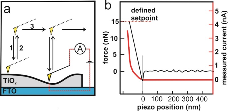
(a) Working principle of the quantitative imaging peak fore-cSFM mode: for each pixel, a single force–distance curve is measured, consisting of an extension (1) and retraction curve (2), before the tip moves to the next pixel (3). A current image is compiled from the maximum current during the extension curves. (b) Exemplary force–distance curve with the respective current curve (red) for a high conducting pixel of an annealed and UV–ozone-treated TiO2 thin film on FTO. In this particular example, a maximum current of 3.6 nA was measured.
To rule out the influence of individual cantilever tips and different measurement conditions, every series of measurements was conducted on the same day within a few hours with the same cantilever. Thereby, we were able to compare absolute values for TiO2 samples, which were prepared for one set of experiments. Although absolute current values varied slightly for different sets of preparations of TiO2 samples, the relative changes were reproducible.
For solar cells, we used a 0.75 M TiCl4 solution (see above) to prepare an approximately 30 nm thick TiO2 anatase layer. In a glovebox with a nitrogen atmosphere, we used a modified standard perovskite precursor solution consisting of 1.2 mol/mL PbI2 (Alfa Aesar, 99.999% metal basis ultra-dry) and MAI (Dyesol) in dimethylformamide (Sigma-Aldrich, 99%) and dimethyl sulfoxide (Sigma-Aldrich 99.5%) with a ratio of 4:1.35 For the hole transport layer (HTL), we dissolved 72.3 mg of 2,2′,7,7′-tetrakis(N,N-di-p-methoxyphenylamino)-9,9′-spirobifluorene (spiro-OMeTAD, Sigma-Aldrich, 99% HPLC), 28.8 μL of tert-butyl pyridine (tBP, Sigma-Aldrich, 96%), and 17.5 μL of Li–bis(trifluoromethanesulfonyl)imide (Sigma-Aldrich 96%) solution (520 mg in 1 mL acetonitrile) in 1 mL of chlorobenzene (Sigma-Aldrich, 99.8%). A volume of 80 μL of the perovskite precursor solution was dispersed on the TiO2-covered substrates. Subsequently, the substrates were spin-coated immediately at 500 rpm for 10 s and 4000 rpm for 25 s. The films were dried at 50 °C for 3 min and annealed at 100 °C for 30 min. After cooling down to room temperature, we dispersed 80 μL of HTL solution on the perovskite film. Then the substrates were spin-coated at 4000 rpm for 15 s. The samples were kept in dry air for 16 h. Finally, we evaporated 50 nm thick gold electrodes on top using a shadow mask with an area of 4 × 4 mm2.
To measure the efficiency of the solar cells, we applied silver paste on each electrode to improve the contact. We used a solar simulator (ASTM class ABA Technologies SunLite TM) with a sourcemeter (Keithley 2400). JV curves were recorded by varying the external bias from −0.1 to 1.2 V with 8.6 mV steps and a scan rate of 43 mV/s for the forward and backward scan. The cells were neither illuminated nor set under an external bias prior to any measurements.
We studied the effect of UV–ozone treatment on the surface by means of X-ray photoelectron spectroscopy (XPS). XPS measurements were carried out with a Kratos Axis Ultra DLD (Kratos Ltd., Manchester, U.K.) using a monochromatic Al Kα X-ray source (1486.6 eV, emission current: 10 mA, anode voltage: 15 kV). The instrument base pressure remained below 1.1 × 10⁻⁹ Pa. The instrument work function was calibrated to a binding energy of 84.0 eV for metallic gold (Au 4f7/2). The charge neutralizer system was used for all measurements. The charge neutralization was monitored for adventitious carbon with the help of the C 1s peak. Survey spectra were recorded at a pass energy of 80 eV with 5 sweeps and an energy step of 1 eV. High-resolution spectra were obtained at a pass energy of 20 eV and 10 sweeps for an energy step of 0.1 eV. The analysis area was ≈300 × 700 μm2. All spectra were recorded in the spectroscopy, hybrid lens mode. For each sample, at least three independent measurements were performed.
Curve synthesis and deconvolution, i.e., identifying the components of the XP signals, were performed by fitting the XP signal with Gaussian/Lorentzian curves. The peak positions for individual components were compared to literature values with the help of the commercial software CasaXPS (version 2.3.16, Casa Software Ltd, Chichester, U.K.). We assumed that only slight deviations from the ideally expected stoichiometric composition of the surface from TiO2 are present (O/Ti = 2:1). For XPS analysis, we used a TiO2 film thickness of 60 nm, and the surface roughness determined by the underlying FTO substrate remained below 10 nm. The binding energies were calibrated using the C 1s peak for adventitious carbon at a binding energy of 284.8 eV, with an associated error of ±0.1–0.2 eV.36 No argon ion sputter cleaning has been performed prior to measurement.
We studied the influence of UV–ozone treatment on the bulk conductance of TiO2 films by THz spectroscopy. This optical pump THz probe setup was driven by an amplified laser system (Solstice ACE by Spectra-Physics). It can produce ultrashort laser pulses of center wavelength 800 nm and a pulse duration of ∼35 fs at a repetition rate of 1 kHz. For the pump beam of this setup, an optical parametric amplifier (TOPAS-Prime and NirUVis by Light Conversion) was used to generate 310 nm pump beam. For the terahertz generation and detection, 10% of the incoming laser beam was used (90 mW). THz radiation was generated in a phase-matched manner by optical rectification on a ZnTe crystal (<110> orientation, 10 × 10 × 1 mm3 thickness, purchased from MaTeck). The ZnTe generation crystal was pumped with an 800 nm beam. The THz light exits the ZnTe generation crystal slightly divergent and is first collimated and subsequently focused on the sample using a pair of off-axis parabolic mirrors. After the sample, the transmitted THz pulses are recollimated and focused onto a second ZnTe detection crystal by another pair of parabolic mirrors, where the instantaneous THz field caused a birefringence that can be detected through electro-optical sampling.37 In this electro-optical sampling, 800 nm laser pulses (<1 mW) with linear polarization were used as a sampling beam. All samples were measured under a nitrogen atmosphere.
Results
To measure the conductance of freshly spin-coated and annealed TiO2 films, we performed cSFM on 60 nm thick TiO2 films made from 1 M TiCl4 solution. This method allows for recording of the local current perpendicularly through the TiO2 thin film—the direction of current propagation in a solar cell device. The spin-coated and annealed TiO2 film showed a maximum current of 7.3 nA at a bias voltage of 1 V over an area of 10 × 10 μm2 (Figure 2a). The surface of this film contains grains with diameters of 10–20 nm and has a root-mean-square (RMS) roughness of 6.9 nm (Figure 2b). This RMS roughness is lower than the roughness of the underlying FTO (RMS of 17.1 nm, Supporting Information).
Figure 2.

(a) Current image and (b) height image of cSFM measurement on the TiO2 thin film without UV–ozone treatment. (c) Current and height image (d) after 30 min of UV–ozone treatment. To visualize local current differences more clearly, we set the current scale to a value of 500 pA. (e) Current distributions before (red data points) and after 30 min UV–ozone treatment (green data points).
After treating this film for 30 min with UV–ozone, we measured a strong increase of the local conductance. Locally, the maximum measurable current even exceeded our maximum detection limit of 120 nA (Figure 2c).
To visualize and compare the local conductance of UV–ozone treated and pristine TiO2 films, we set the current scale to 0–500 pA (Figure 2a, c). For the untreated surface, we obtained <0.1% pixels with a current >500 pA. For the treated surface, we obtained 45.8% pixels with a current >500 pA. Furthermore, the conductance of the treated film is distributed more homogeneously over the surface compared to the untreated film. To compare the changes in conductance after treatment, we calculated the normalized current distribution (ρ) by dividing each value by the sum (Figure 2e). Then, we calculated the median value. For the untreated sample, the median value was 4.6 pA (red dashed lines in Figure 2e) and for the UV–ozone treated sample the median was 378 pA (green dashed lines in Figure 2e). Therefore, the median increased by roughly 2 orders of magnitude after UV–ozone treatment.
We repeated the comparison of untreated and treated films several times with different samples prepared in an identical manner (Supporting Information). In all cases, we found an increase by 2 orders of magnitude in the median value of the conductance distribution after UV–ozone treatment. In addition, the UV–ozone cleaning is not associated with a change in surface roughness (Figure 2d; RMS is 7.8 nm). We can also exclude a reduction in TiO2 film thickness: without treatment, we measured a film thickness of 61.8 ± 1.1 and 61.5 ± 1.2 nm after 30 min of UV–ozone treatment. This shows that a simple UV–ozone treatment can increase the conductance through the TiO2 film without altering the surface roughness or film thickness (Supporting Information).
It is well-known that cSFM is sensitive to changes in the tip–sample contact area. A higher tip–sample contact area would collect more charge carriers and thus the current would increase. However, current maps were reproducible for tips used for approximately 3.5 million force–distance curves (50 images) and fresh ones in the QI-mode (Supporting Information). Therefore, we exclude significant changes of tip–sample contact area during imaging.
The SFM-tip has a Pt/Ir-metal coating with a work function of ∼3.9 eV.34 The semiconducting anatase form of TiO2 has a work function of 5.1 eV.38 Therefore, we expect a Schottky-diode-characteristic IV behavior with an onset in current at around 1.2 V. For a UV–ozone treatment, we do not expect a change of this diode behavior since neither the roughness nor the thickness of the TiO2 film changes. To rule out possible local short circuits or other effects such as the generation of local failure of electron transport or hole blocking behavior, we measured the I–V characteristics of a sample that was annealed and UV–ozone treated (Figure 3). For this, we measured consecutive cSFM on the same substrate with varying external bias. We plotted the measured median current against the applied bias to generate an I–V-curve. Our measurements revealed a reproducible diode behavior for both forward and backward scan. A current below the noise level of our cSFM of 1.5 pA was measured at an external bias below 0.75 V. Thus, we preserve the diode properties of the TiO2 layer during UV–ozone treatment.
Figure 3.

Normalized local I–V-curves of an annealed and UV–ozone-treated TiO2 film on FTO. Measurements were conducted starting at an initial bias of +1.5 V, which was increased stepwise to 0 V and then inverted up to −1.5 V (black curve). Subsequently, the bias was reduced stepwise again to 0 V and inverted up to 1.5 V (red curve). Please note that for every image a new area of 256 × 256 pixels was measured to avoid any potential influence of previous measurements. This set of measurement took approximately 1 h.
TiO2 surfaces were contaminated with hydrocarbons within a few hours when kept in air.39 Such hydrocarbon adsorbates change surface properties and the local conductance.40 To examine this effect, we performed consecutive cSFM control measurements on a freshly prepared and UV–ozone-treated sample over a period of 12 h. We found a decrease of the median current by 50% after 3 h (Figure 4). After 12 h, the median current value had dropped to 12% of the initial value. Therefore, we suggest that TiO2 surfaces should be processed directly after annealing and UV–ozone cleaning.
Figure 4.

Development of median current over time for a freshly prepared and UV ozone treated TiO2 film.
The increase in the perpendicular conductance of TiO2 by the UV–ozone treatment as probed by cSFM is expected to affect the PCE of perovskite solar cells. Therefore, we fabricated 61 planar perovskite-based solar cells based on standard protocols from the literature as described in detail in the Experimental Section.35 To verify the relevance for PSC, half of these cells were made with TiO2 that was exposed for 30 min to UV–ozone. For the other half, we used TiO2 films directly after the annealing step, a typical protocol for many of today’s standard processes.41 For all cells, we measured the short-circuit current density Jsc, the open-circuit potential Voc, and the fill factor (FF), and we calculated the PCE.
Cells made with the freshly annealed TiO2 without UV–ozone treatment showed an average Jsc of 20.5 ± 3.1 mA/cm2 (Table 1). The cells with UV–ozone-treated TiO2 layers showed an average Jsc of 21.9 ± 1.5 mA/cm2. Thus, the increased local conductance through the TiO2 film led to an increased Jsc by approx. 10%. We explain the increase in Jsc with an increasing collection probability of charge carriers into the TiO2 layer upon removing surface traps. In addition, the standard deviation of the Jsc decreased, which hints to a more uniform and reproducible preparation process. The open-circuit voltage changed only slightly (Table 1). We also measured an increase in the FF from 63.8 ± 8.3 to 68.2 ± 4.0 for the UV–ozone-treated cells. We attribute the latter to a decreased internal serial resistance through the layers. The higher Jsc and FF for the UV–ozone-treated cells resulted in an increase in average PCE from 13.8 ± 3.1 to 15.9 ± 1.9% (Table 1 and Figure 5). With UV–ozone treatment, we fabricated a champion cell with an efficiency of 19.1%. Without UV–ozone treatment, the champion cell had an efficiency of 18.5%.
Table 1. Parameters of Treated and Untreated Perovskite Solar Cells with Compact TiO2 Layers as ETLsa.
| device | Jsc (mA/cm2) | Voc (mV) | FF (%) | PCE (%) | |
|---|---|---|---|---|---|
| annealed and UVO treated | mean value | (21.9 ± 1.5) | (1061 ± 42) | (68.2 ± 4.0) | (15.9 ± 1.9) |
| champion | 23.0 | 1098 | 75.8 | 19.1 | |
| annealed | mean value | (20.5 ± 3.1) | (1052 ± 58) | (63.8 ± 8.3) | (13.8 ± 3.1) |
| champion | 23.2 | 1088 | 73.4 | 18.5 |
Displayed are the mean values of the short-circuit current Jsc, the open-circuit voltage Voc, the fill factor FF, and the power conversion efficiency PCE.
Figure 5.

Distribution of cell efficiency without UV–ozone and with UV–ozone treatment.
UV–ozone treatment also has a beneficial effect on mesoporous TiO2 ETLs (Table 2) and other metal oxide-based ETLs, such as SnO2 (Table 3). For mesoporous TiO2 films, we measured an increase of 1.2 percentage points in the average PCE after UV–ozone treatment with a record cell efficiency of 19.5%. These PCE represents the state-of-the-art for single halide single cation perovskite solar cells, i.e., MAPbI3 on mesoporous TiO2.42 For a compact SnO2 ETL, UV–ozone treatment improved the average PCE by 1.6% (absolute). Thus, the UV–ozone cleaning step can also be applied to other metal oxide-based ETL.
Table 2. Parameters of Treated and Untreated Perovskite Solar Cells with Compact and Mesoporous TiO2 Layers as ETLs.
| device | Jsc (mA/cm2) | Voc (mV) | FF (%) | PCE (%) | |
|---|---|---|---|---|---|
| annealed and UVO treated | mean value | (23.7 ± 0.6) | (1059 ± 3) | (75.4 ± 0.7) | (18.9 ± 0.4) |
| champion | 24.7 | 1054.2 | 74.9 | 19.5 | |
| annealed | mean value | (23.6 ± 0.5) | (1060 ± 9) | (70.7 ± 5.9) | (17.7 ± 1.4) |
| champion | 23.9 | 1050.2 | 74.5 | 18.7 |
Table 3. Parameters of Treated and Untreated Perovskite Solar Cells with Compact SnO2 Layers as ETLs.
| device | Jsc (mA/cm2) | Voc (mV) | FF (%) | PCE (%) | |
|---|---|---|---|---|---|
| annealed and UVO treated | mean value | (21.2 ± 0.3) | (1068 ± 4) | (73.5 ± 1.1) | (16.6 ± 0.4) |
| champion | 21.2 | 1070 | 75.1 | 17.0 | |
| annealed | mean value | (20.4 ± 1.8) | (1059 ± 10) | (69.2 ± 2.4) | (15.0 ± 1.6) |
| champion | 21.9 | 1071 | 71.9 | 16.9 |
We performed XPS analysis on samples prepared according to three different procedures: (1) Freshly prepared samples that were directly transferred to the vacuum prechamber of the XPS instrument, i.e., the freshly annealed sample. (2) Freshly prepared samples that were directly subjected to UV–ozone treatment and then transferred immediately to the XPS instrument, i.e., UV–ozone sample. (3) Samples that had been prepared 24 h earlier without UV–ozone treatment and subsequently exposed to an ambient atmosphere for 24 h, i.e., the annealed sample after 24 h.
To investigate the role of unspecific unpolar insulating hydrocarbons on the surface of TiO2, we analyzed the C 1s high-resolution XP-spectra. We found no significant difference in the peak shape of the high-resolution C 1s XP signals between annealed-only and annealed plus UV–ozone-treated samples (Supporting Information). The relative intensity of the individual contributions, and hence the peak shape of the overall C 1s XP signal did not change due to UV–ozone treatment. However, we observed a significant difference in the peak shape between the freshly prepared samples (a and b), and the samples that had been exposed to ambient air for 24 h (c). We conclude that the UV–ozone treatment on freshly made and annealed TiO2 films had no impact on the presence of hydrocarbons and thus could not be the reason for the increase of the measured local conductance. Therefore, the UV–ozone treatment alters the surface in a different way.
The O 1s signals are known to be affected by oxygen treatment.27,23,28 The O 1s signals contain three contributions (Table 4). (i) A signal at 530.0 eV corresponds to oxygen that is bound to coordinatively saturated titanium atoms (red curve Figure 6). (ii) At an energy of 531.1 eV, the signal is caused by oxygen that is bound to partly unsaturated titanium atoms. This signal corresponds to the number of oxygen vacancies (blue curve Figure 6). (iii) A signal at 532.2 eV originates from oxygen in −OH groups and adsorbed CO2 (green curve Figure 6).23
Table 4. Influence of UV–Ozone Treatment or Storage at Ambient Conditions on O 1s Signalsa.
| O bound to saturated Ti (I) | O bound to unsaturated Ti (II) | –OH and CO2 groups (III) | |
|---|---|---|---|
| annealed | 77% | 15% | 8% |
| annealed and UV–ozone treated | 82% | 9% | 9% |
| annealed after 24 h | 59% | 15% | 26% |
For the freshly annealed samples, we calculated the following energies: (I) 530.0 eV, (II) 531.1 eV, and 532.2 eV. For the annealed and UV–ozone-treated sample, peak maxima were calculated at (I) 530.1 eV, (II) 530.9 eV, and (III) 532.0 eV. For the annealed samples that were kept in ambient conditions for 24 h, we calculated the following energies: (I) 530.1 eV, (II) 531.6 eV, and 532.2 eV.
Figure 6.

Effect of UV–ozone treatment on the number of surface oxygen vacancies. The measured signals (black curves) were fitted with three Gaussian/Lorentzian curves. The red curves correspond to oxygen bound to coordinatively saturated titanium atoms. The blue curves correspond to oxygen that is bound to partly unsaturated titanium atoms. The green curves correspond to oxygen in −OH groups and adsorbed CO2. (a) annealed sample, (b) annealed and UV–ozone treated, (c) annealed after 24 h.
For the annealed sample, the most intense contribution to the O 1s signal originates from oxygen that is bound to coordinatively saturated titanium atoms (Figure 4a); we calculated a relative peak area of ∼77% for (i). The signal corresponding to oxygen that is bound to partly unsaturated titanium atoms covers a peak area of ∼15% (ii). The O 1s signal from −OH groups and adsorbed CO2 corresponds to a peak area of ∼8% (iii).
For the annealed and UV–ozone treated sample, we calculated relative peak areas of 82% at 530.1 eV (i), ∼9% at 530.9 eV (ii), and 9% at 532.0 eV (iii). The change in the relative peak area reflects a change in stoichiometry. The amount of oxygen bound to partly unsaturated titanium atoms in the lattice decreases. This decrease means that the number of surface oxygen vacancies at the surface decreases.
For the annealed sample that was kept 24 h in ambient conditions, we calculated relative peak areas of ∼59% at 530.1 eV (i), ∼15% at 531.6 eV (ii), and 26% at 532.2 eV (iii). Compared to the annealed sample and the UV–ozone sample, the contribution of oxygen that is bound to coordinatively saturated titanium atoms (i) is reduced considerably. A significantly increased number of surface-bound −OH and CO2 oxygen groups are found compared to both freshly annealed samples. We interpret this as an indication not only for the adsorption of water and carbon dioxide but also as a general indication for the presence of adsorbed species on the TiO2 surface, showing the recontamination after being stored at ambient conditions for 1 day. The relative intensity of the contribution originating from oxygen that is bound to partly unsaturated titanium atoms (ii) remains unchanged compared to the annealed sample.
The O 1s signal that corresponds to oxygen that is bound to partly unsaturated titanium atoms (i) is slightly shifted to the higher binding energy. It has been shown, that carbon species adsorb more strongly on partly reduced TiO2 surfaces, which corresponds to more oxygen vacancies.43 Thus, we argue that the shift reflects surface oxygen vacancies acting as reactive centers, which react preferably with hydrocarbons and thereby change the chemical environment locally.
Our XPS results suggest that UV–ozone treatment reduces the number of surface oxygen vacancies. We could show that a reduction of surface oxygen vacancies correlates with an increased conductance through a TiO2 thin film. This finding is interesting, as oxygen vacancies are usually regarded as only beneficial for the conductance of TiO2 crystals since these vacancies act as n-doping within the lattice.15 We emphasize that the overall conductance of a TiO2 thin film is determined by both surface and bulk and that oxygen vacancies can either be beneficial for the conductance (when located in the bulk) or disadvantageous (when located at the interface).
To show that the beneficial effect of UV–ozone treatment is solely due to a surface effect, we conducted terahertz experiments to measure changes in the bulk conductance of TiO2 films on fused silica. Experimentally, we measured the THz field E in the time domain that was transmitted through the nonexcited sample and the photoinduced change ΔE from the excited sample. The optical conductance Δσ can be calculated by
| 1 |
where n, Z0, and l are the refractive index of fused silica (n = 1.95), the impedance of free space (Z0 = 377 Ω), and the thickness of the samples (for this experiment 250 nm), respectively. For the sample that was only annealed, we measured an optical conductance of ∼51 S/m after a pump-probe delay of 1 ps. The additional UV–ozone cleaning led to a slight decrease of conductance to ∼46 S/m (Figure 7). This decrease corresponds to a slight reduction in the number of n-dopants in the TiO2 bulk material.
Figure 7.

Influence of UV–ozone treatment on optical conductance of a TiO2 thin film on quartz glass.
We draw two conclusions from this measurement. First, the location of an oxygen vacancy is crucial for its influence on the conductance of TiO2. In bulk, oxygen vacancies leads to n-type conductivity. However, at the interface of a TiO2 film, the oxygen vacancy act as an electron trap that decreases the conductance. Second, we could show that, for TiO2 films, bulk conductance is not a dominating factor for the measured conductance. The slight decrease in bulk conductance is overcompensated by the beneficial effect of removing the surface oxygen vacancies.
Conclusions
Many research groups working in the field of solar cell development are processing TiO2 directly after annealing, assuming that the freshly annealed surface is optimal for the fabrication of PSC. We show that an additional UV–ozone treatment increases the local conductance through a TiO2 anatase film by 2 orders of magnitude. UV–ozone treatment causes only a negligible decrease in bulk conductance. This decrease is overcompensated by the effect of the surface conductance. Surface oxygen vacancies create surface states that act as a potential barrier and thus increase the series electrical resistance through both surface and bulk.7 Removal of these oxygen vacancies leads to an increase of the overall conductance. XPS measurements confirm that UV–ozone-treatment reduces the number of surface oxygen vacancies. Furthermore, hydrocarbon contaminations play only a minor role when the samples are investigated directly after annealing or UV–ozone treatment.
Importantly, the additional UV–ozone-treatment leads to an increase in Jsc and the fill factor of planar perovskite solar cells and increased the PCE by approx. 2%. With this refined preparation process, we created a champion cell PCE of 19.1%. The additional UV–ozone-treatment is similarly beneficial for PSCs based on mesoporous TiO2 and planar SnO2.
Acknowledgments
The authors thank Gabriele Hermann and Hao Lu for the XPS experiments and Michael Steiert for the X-ray diffraction measurements. We are grateful to Selim Basaran for the support and fruitful discussions. We thank the DFG (BE 3286/4-1) for financially supporting this project. P.B. acknowledges the funding received from the European Union’s Horizon 2020 research and innovation program under the Marie Skłodowska-Curie grant agreement No. 722497 (ITN LubISS). I.M.H. acknowledges ERC Grant No. 340391 SuPro for funding.
Supporting Information Available
The Supporting Information is available free of charge on the ACS Publications website at DOI: 10.1021/acs.jpcc.9b02371.
(i) Preparation of aqueous TiCl4 solution; (ii) influence of UV–ozone treatment time on measured median current; (iii) influence of sample erosion on measured median current; (iv) influence of tip erosion on measured median current; (v) solar cell parameters of forward and backward scan; (vi) comparison of C 1s XP spectra of a freshly annealed, a freshly annealed and UV–ozone treated and an annealed sample after 24 h in ambient conditions (PDF)
Author Contributions
This manuscript was written through contributions of all authors. All authors have given approval for the final version of the manuscript.
The authors declare no competing financial interest.
Supplementary Material
References
- Fathil M. F. M.; Adzhri R.; Arshad M. K. M.; Hashim U.; Ruslinda A. R.; Ayub R. M.; Nuzaihan M. N. M.; Azman A. H.; Zaki M. In Preparation and Characterization of Titanium Dioxide Thin Film for Field-Effect Transistor Biosensor Application, 2015 2nd International Conference on Biomedical Engineering (ICoBE), 2015; pp 30–31.
- Hu S.; Shaner M. R.; Beardslee J. A.; Lichterman M.; Brunschwig B. S.; Lewis N. S. Amorphous TiO2 Coatings Stabilize Si, GaAs, and GaP Photoanodes for Efficient Water Oxidation. Science 2014, 344, 1005–1009. 10.1126/science.1251428. [DOI] [PubMed] [Google Scholar]
- Li M.; Li X.; Li W.; Meng X.; Yu Y.; Sun X. Atomic Layer Deposition Derived Amorphous TiO2 Thin Film Decorating Graphene Nanosheets with Superior Rate Capability. Electrochem. Commun. 2015, 57, 43–47. 10.1016/j.elecom.2015.05.005. [DOI] [Google Scholar]
- Dongale T. D.; Shinde S. S.; Kamat R. K.; Rajpure K. Y. Nanostructured TiO2 Thin Film Memristor Using Hydrothermal Process. J. Alloys Compd. 2014, 593, 267–270. 10.1016/j.jallcom.2014.01.093. [DOI] [Google Scholar]
- Yu J.; Zhao X.; Zhao Q. Effect of Surface Structure on Photocatalytic Activity of TiO2 Thin Films Prepared by Sol-Gel Method. Thin Solid Films 2000, 379, 7–14. 10.1016/S0040-6090(00)01542-X. [DOI] [Google Scholar]
- Rahman M. A.; Bazargan S.; Srivastava S.; Wang X.; Abd-Ellah M.; Thomas J. P.; Heinig N. F.; Pradhan D.; Leung K. T. Defect-Rich Decorated TiO2 Nanowires for Super-Efficient Photoelectrochemical Water Splitting Driven by Visible Light. Energy Environ. Sci. 2015, 8, 3363–3373. 10.1039/C5EE01615K. [DOI] [Google Scholar]
- Xing G.; Wu B.; Chen S.; Chua J.; Yantara N.; Mhaisalkar S.; Mathews N.; Sum T. C. Interfacial Electron Transfer Barrier at Compact TiO2CH3NH3PbI3 Heterojunction. Small 2015, 11, 3606–3613. 10.1002/smll.201403719. [DOI] [PubMed] [Google Scholar]
- Mercado C. C.; Knorr F. J.; McHale J. L.; Usmani S. M.; Ichimura A. S.; Saraf L. V. Location of Hole and Electron Traps on Nanocrystalline Anatase TiO2. J. Phys. Chem. C 2012, 116, 10796–10804. 10.1021/jp301680d. [DOI] [Google Scholar]
- Zhang Z.; Yates J. T. Jr. Direct Observation of Surface-Mediated Electron-Hole Pair Recombination in TiO2 (110). J. Phys. Chem. C 2010, 114, 3098–3101. 10.1021/jp910404e. [DOI] [Google Scholar]
- Singh T.; Singh J.; Miyasaka T. Role of Metal Oxide Electron-Transport Layer Modification on the Stability of High Performing Perovskite Solar Cells. ChemSusChem 2016, 9, 2559–2566. 10.1002/cssc.201601004. [DOI] [PubMed] [Google Scholar]
- Zhang P.; Wu J.; Zhang T.; Wang Y.; Liu D.; Chen H.; Ji L.; Liu C.; Ahmad W.; Chen Z. D.; et al. Perovskite Solar Cells with ZnO Electron-Transporting Materials. Adv. Mater. 2018, 30, 1703737 10.1002/adma.201703737. [DOI] [PubMed] [Google Scholar]
- You J.; Meng L.; Song T.-B.; Guo T.-F.; Yang Y.; Chang W.-H.; Hong Z.; Chen H.; Zhou H.; Chen Q.; et al. Improved Air Stability of Perovskite Solar Cells via Solution-Processed Metal Oxide Transport Layers. Nat. Nanotechnol. 2016, 11, 75–81. 10.1038/nnano.2015.230. [DOI] [PubMed] [Google Scholar]
- Dong X.; Hu H.; Lin B.; Ding J.; Yuan N. The Effect of ALD-Zno Layers on the Formation of CH3NH3PbI3 with Different Perovskite Precursors and Sintering Temperatures. Chem. Commun. 2014, 50, 14405–14408. 10.1039/C4CC04685D. [DOI] [PubMed] [Google Scholar]
- Green M. A.; Hishikawa Y.; Dunlop E. D.; Levi D. H.; Hohl-Ebinger J.; Yoshita M.; Ho-Baillie A. W. Y. Solar Cell Efficiency Tables (Version 53). Prog. Photovoltaics: Res. Appl. 2019, 27, 3–12. 10.1002/pip.3102. [DOI] [Google Scholar]
- Diebold U. The Surface Science of Titanium Dioxide. Surf. Sci. Rep. 2003, 48, 53–229. 10.1016/S0167-5729(02)00100-0. [DOI] [Google Scholar]
- Liu C.; Wang K.; Du P.; Meng T.; Yu X.; Cheng S. Z. D.; Gong X. High Performance Planar Heterojunction Perovskite Solar Cells with Fullerene Derivatives as the Electron Transport Layer. ACS Appl. Mater. Interfaces 2015, 7, 1153–1159. 10.1021/am506869k. [DOI] [PubMed] [Google Scholar]
- Leijtens T.; Lim J.; Teuscher J.; Park T.; Snaith H. J. Charge Density Dependent Mobility of Organic Hole-Transporters and Mesoporous TiO2 Determined by Transient Mobility Spectroscopy: Implications to Dye-Sensitized and Organic Solar Cells. Adv. Mater. 2013, 25, 3227–3233. 10.1002/adma.201300947. [DOI] [PubMed] [Google Scholar]
- Kawakami R.; Yuasa T.; Sato Y.; Mori Y. Effects of Particle Size on Properties of TiO2 Nanoparticle Thin Films Deposited by Electrophoresis. Key Eng. Mater. 2013, 566, 199–203. 10.4028/www.scientific.net/KEM.566.199. [DOI] [Google Scholar]
- Ye T.; Xing J.; Petrović M.; Chen S.; Chellappan V.; Subramanian G. S.; Sum T. C.; Liu B.; Xiong Q.; Ramakrishna S. Temperature Effect of the Compact TiO2 Layer in Planar Perovskite Solar Cells: An Interfacial Electrical, Optical and Carrier Mobility Study. Sol. Energy Mater. Sol. Cells 2017, 163, 242–249. 10.1016/j.solmat.2017.01.005. [DOI] [Google Scholar]
- Hermes I. M.; Hou Y.; Bergmann V. W.; Brabec C. J.; Weber S. A. L. The Interplay of Contact Layers: How the Electron Transport Layer Influences Interfacial Recombination and Hole Extraction in Perovskite Solar Cells. J. Phys. Chem. Lett. 2018, 9, 6249–6256. 10.1021/acs.jpclett.8b02824. [DOI] [PubMed] [Google Scholar]
- Weber S. A. L.; Hermes I. M.; Turren-Cruz S. H.; Gort C.; Bergmann V. W.; Gilson L.; Hagfeldt A.; Graetzel M.; Tress W.; Berger R. How the Formation of Interfacial Charge Causes Hysteresis in Perovskite Solar Cells. Energy Environ. Sci. 2018, 11, 2404–2413. 10.1039/C8EE01447G. [DOI] [Google Scholar]
- Olthof S.; Meerholz K. Substrate-Dependent Electronic Structure and Film Formation of MAPbI3 Perovskites. Sci. Rep. 2017, 7, 40267 10.1038/srep40267. [DOI] [PMC free article] [PubMed] [Google Scholar]
- Ma X.; Tang P.; Liu D.; Wu L.; Zhang J.; Feng L. Interface Engineering of Perovskite Solar Cells with Air Plasma Treatment for Improved Performance. ChemPhysChem 2017, 18, 2939–2946. 10.1002/cphc.201700536. [DOI] [PubMed] [Google Scholar]
- Liu G.; Yang B.; Liu B.; Zhang C.; Xiao S.; Yuan Y.; Xie H.; Niu D.; Yang J.; Gao Y.; et al. Irreversible Light-Soaking Effect of Perovskite Solar Cells Caused by Light-Induced Oxygen Vacancies in Titanium Oxide. Appl. Phys. Lett. 2017, 111, 153501 10.1063/1.4994085. [DOI] [Google Scholar]
- Cojocaru L.; Uchida S.; Sanehira Y.; Nakazaki J.; Kubo T.; Segawa H. Surface Treatment of the Compact TiO2 Layer for Efficient Planar Heterojunction Perovskite Solar Cells. Chem. Lett. 2015, 44, 674–676. 10.1246/cl.150068. [DOI] [Google Scholar]
- Ke W.; Fang G.; Wan J.; Tao H.; Liu Q.; Xiong L.; Qin P.; Wang J.; Lei H.; Yang G.; et al. Efficient Hole-Blocking Layer-Free Planar Halide Perovskite Thin-Film Solar Cells. Nat. Commun. 2015, 6, 6700 10.1038/ncomms7700. [DOI] [PubMed] [Google Scholar]
- Kim I. S.; Haasch R. T.; Cao D. H.; Farha O. K.; Hupp J. T.; Kanatzidis M. G.; Martinson A. B. F. Amorphous TiO2 Compact Layers via ALD for Planar Halide Perovskite Photovoltaics. ACS Appl. Mater. Interfaces 2016, 8, 24310–24314. 10.1021/acsami.6b07658. [DOI] [PubMed] [Google Scholar]
- Chong H. Y.; Lee S. H.; Kim T. W. Effect of an Ultraviolet-Ozone Treatment on the Electrical Properties of Titanium-Oxide Thin-Film Transistors Fabricated by Using a Sol-Gel Process. J. Electrochem. Soc. 2012, 159, B771–B774. 10.1149/2.016207jes. [DOI] [Google Scholar]
- Liau Y.; Scherer N. F.; Rhodes K. Nanoscale Electrical Conductivity and Surface Spectroscopic Studies of Indium - Tin Oxide. J. Phys. Chem. B 2001, 105, 3282–3288. 10.1021/jp0040749. [DOI] [Google Scholar]
- Li J.-J.; Ma J.-Y.; Ge Q.-Q.; Hu J.-S.; Wang D.; Wan L.-J. Microscopic Investigation of Grain Boundaries in Organolead Halide Perovskite Solar Cells. ACS Appl. Mater. Interfaces 2015, 7, 28518–28523. 10.1021/acsami.5b09801. [DOI] [PubMed] [Google Scholar]
- Hieulle J.; Stecker C.; Ohmann R.; Ono L. K.; Qi Y. Scanning Probe Microscopy Applied to Organic-Inorganic Halide Perovskite Materials and Solar Cells. Small Methods 2017, 2, 1700295 10.1002/smtd.201700295. [DOI] [Google Scholar]
- Moerman D.; Eperon G. E.; Precht J. T.; Ginger D. S. Correlating Photoluminescence Heterogeneity with Local Electronic Properties in Methylammonium Lead Tribromide Perovskite Thin Films. Chem. Mater. 2017, 29, 5484–5492. 10.1021/acs.chemmater.7b00235. [DOI] [Google Scholar]
- Tennyson E.; Leite M. Mapping the Performance of Solar Cells with Nanoscale Resolution. SPIE Newsroom 2015, 1, 10–12. 10.1117/2.1201509.006097. [DOI] [Google Scholar]
- Sharma A.; Untch M.; Quinton J. S.; Berger R.; Andersson G.; Lewis D. A. Nanoscale Heterogeniety and Workfunction Variations in ZnO Thin Films. Appl. Surf. Sci. 2016, 363, 516–521. 10.1016/j.apsusc.2015.11.190. [DOI] [Google Scholar]
- Ahn N.; Son D. Y.; Jang I. H.; Kang S. M.; Choi M.; Park N. G. Highly Reproducible Perovskite Solar Cells with Average Efficiency of 18.3% and Best Efficiency of 19.7% Fabricated via Lewis Base Adduct of Lead(II) Iodide. J. Am. Chem. Soc. 2015, 137, 8696–8699. 10.1021/jacs.5b04930. [DOI] [PubMed] [Google Scholar]
- Miller D. J.; Biesinger M. C.; McIntyre N. S. Interactions of CO2 and CO at Fractional Atmosphere Pressures with Iron and Iron Oxide Surfaces: One Possible Mechanism for Surface Contamination?. Surf. Interface Anal. 2002, 33, 299–305. 10.1002/sia.1188. [DOI] [Google Scholar]
- Jensen S. A.Charge Carrier Dynamics in Photovoltaic Materials; Universiteit van Amsterdam, 2014. [Google Scholar]
- Scanlon D. O.; Dunnill C. W.; Buckeridge J.; Shevlin S. A.; Logsdail A. J.; Woodley S. M.; Catlow C. R. A.; Powell M. J.; Palgrave R. G.; Parkin I. P.; et al. Band Alignment of Rutile and Anatase TiO2. Nat. Mater. 2013, 12, 798–801. 10.1038/nmat3697. [DOI] [PubMed] [Google Scholar]
- Park K. H.; Dhayal M. High Efficiency Solar Cell Based on Dye Sensitized Plasma Treated Nano-Structured TiO2 Films. Electrochem. Commun. 2009, 11, 75–79. 10.1016/j.elecom.2008.10.020. [DOI] [Google Scholar]
- Lacasa J. S.; Almonte L.; Colchero J. In Situ Characterization of Nanoscale Contaminations Adsorbed in Air Using Atomic Force Microscopy. Beilstein J. Nanotechnol. 2018, 9, 2925–2935. 10.3762/bjnano.9.271. [DOI] [PMC free article] [PubMed] [Google Scholar]
- Saliba M.; Correa-Baena J. P.; Wolff C. M.; Stolterfoht M.; Phung N.; Albrecht S.; Neher D.; Abate A. How to Make over 20% Efficient Perovskite Solar Cells in Regular (n-i-p) and Inverted (p-i-n) Architectures. Chem. Mater. 2018, 30, 4193–4201. 10.1021/acs.chemmater.8b00136. [DOI] [Google Scholar]
- Grätzel M.; Hagfeldt A.; Saliba M.; Tress W.; Correa-Baena J.-P.; Abate A.; Buonassisi T. Promises and Challenges of Perovskite Solar Cells. Science 2017, 358, 739–744. 10.1126/science.aam6323. [DOI] [PubMed] [Google Scholar]
- Petrik N. G.; Zhang Z.; Du Y.; Dohna Z.; Lyubinetsky I.; Kimmel G. A. Chemical Reactivity of Reduced TiO2 ( 110 ): The Dominant Role of Surface Defects in Oxygen Chemisorption. J. Phys. Chem. C 2009, 2, 12407–12411. 10.1021/jp901989x. [DOI] [Google Scholar]
Associated Data
This section collects any data citations, data availability statements, or supplementary materials included in this article.