Abstract
Defect energetics, charge transition levels, and electronic band structures of several Cl-related complexes in CdTe are studied using density-functional theory calculations. We investigate substitutional chlorine (ClTe and ClCd) and complexes formed by ClTe with the cadmium vacancy (ClTe-VCd and 2ClTe-VCd) and the TeCd antisite (ClTe-TeCd). Our calculations show that none of the complexes studied induce deep levels in the CdTe band gap. Moreover, we find that ClTe-VCd and ClTe are the most stable Cl-related centers in n-type and p-type CdTe, under Te-rich growth conditions, showing shallow donor and acceptor properties, respectively. This result suggests that the experimentally-observed Fermi level pinning near midgap would be originated in self-compensation. We also find that the formation of the ClTe-TeCd complex passivates the deep level associated to the Te antisite in neutral charge state.
Subject terms: Semiconductors, Electronic properties and materials
Introduction
Cadmium telluride (CdTe) is a II-VI chalcogenide semiconductor with a band gap energy of ∼1.5 eV at room temperature, being one of the few that can be relatively easily doped p- and n-type. CdTe has been actively investigated for more than 70 years for photovoltaics1–3, room-temperature γ- and x-ray radiation detection4–7, as well as medical imaging8. Due to its high stability (formation enthalpy ∼100 kJ mol−1), high absorption coefficient (>5 × 105 cm−1), and near optimum band gap for visible absorption, CdTe is very suitable material for use as absorber layer in thin-film solar cells. In fact, single-junction CdTe-based solar cells have recently reached conversion efficiencies as high as 22.1%9. Additionally, its low manufacturing cost and the continuing improvement on its conversion efficiency have positioned CdTe among one of the most promising materials alternative to crystalline silicon, which dominates the global photovoltaic market10.
In addition, the large CdTe band gap allows its use in γ- and x-ray detectors, operating at room temperature with modest cooling11, as opposed to germanium-based detectors that require cryogenic temperatures to operate. Moreover, high-quality radiation detectors require an intrinsic high resistivity to reduce dark currents, a high mobility-lifetime product of electrons (μτ), and a high atomic weight12. The former property can be achieved in CdTe by self-compensation of intrinsic point defects during the crystal growth, while the latter are guaranteed by its good charge transport properties and large atomic number of its constituents.
It is widely known that native defects usually play an important role by limiting the p- or n-type conductivity in a semiconductor13–17, which may be achieved by extrinsic doping18,19. Due to its importance and the complexity of the problem, understanding the effect of self-compensation in CdTe is a major focus of current research in the field15,20–23. Moreover, in the case of CdTe, group IV elements can be used as extrinsic dopants to achieve a semi-insulating material24–27. However, these impurities normally introduce deep levels in the band gap, which may act as non-radiative Shockley-Read-Hall recombination centers28,29 with a deleterious effect on the performance of the detector. This does not apply to chlorine doping of CdTe, which results in a high-resistive material with good carrier transport properties30,31, suitable for γ- and x-radiation detection32,33; still, the origin of its electric properties is not well understood and remains as an open issue34.
The dominant compensation model for detector-grade CdTe:Cl is based on the existence of one compensating deep level located at ∼0.725 eV above the valence band maximum (VBM)12,34, which might be responsible for the Fermi level pinning near midgap. This model is supported by experimental observations, but it cannot be explained by theory. In this context, several theoretical works have suggested that compensation between shallow donors and acceptors, rather than one deep level, should be responsible for the Fermi level pinning in CdTe:Cl35,36. However, other works have concluded that high-resistivity in CdTe:Cl cannot be explained by shallow defect levels alone37.
In this work, we set out to determine the origin of the high-resistivity experimentally observed in detector-grade CdTe:Cl. In that aim, we calculate from ab-initio the formation energies, electronic structure, and transition states of three chlorine-related defects in CdTe: (i) the isolated substitutional chlorine, that is Cl occupying a Te site (ClTe) and a Cd site (ClCd); (ii) the two complexes formed by ClTe nearest neighbor to the cadmium vacancy (VCd). The first one contains one ClTe neighboring to the vacancy (ClTe-VCd), which is commonly known as the A-center, while the second one contains two ClTe neighboring to the vacancy (2ClTe-VCd); and (iii) the complex formed by the ClTe impurity nearest neighbor to the TeCd antisite (ClTe-TeCd). Our results show that ClTe-VCd is the most stable Cl-related complex in n-type CdTe, that together with ClTe, the most stable Cl impurity in p-type CdTe, would play a key role in the self-compensation mechanism. Indeed, our results support the hypothesis that compensation between shallow donors and acceptors alone can explain the good electron mobility and high-resistivity of CdTe:Cl, in agreement with experimental observations.
Results and Discussion
Substitutional chlorine in CdTe
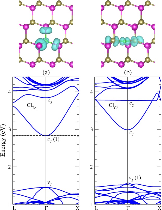
As an isolated substitutional impurity, chlorine can occupy only a Cd site or a Te site in CdTe. Our initial model was simply substitute a lattice atom with the neutral Cl impurity and left the system to relax. Figure 1(a) shows the equilibrium geometries and band structure of substitutional chlorine in CdTe in the neutral charge state. Our results for chlorine occupying a Te site (ClTe) indicate a four-fold coordinated impurity with almost undistorted geometry, preserving the Td symmetry. The Cd atoms next to the impurity relax outwards by about 3%, resulting in a Cd-Cl bond distance of 2.936 Å. The same configuration is observed in single positive charge state. The electronic properties indicate that ClTe is a shallow donor, introducing an impurity level resonant in the conduction band (c2). The squared wavefunction, or simply the charge density, corresponding to this level indicates a Cl-Cd antibonding character, as shown Fig. 1(a). The electronic structure shows a band gap of 1.40 eV, close to that calculated for pristine CdTe (1.44 eV).
Figure 1.
Equilibrium geometry and band structure calculations of substitutional chlorine in the neutral charge state. (a) ClTe, and (b) ClCd. The dashed line indicates the Fermi energy. Charge density isosurface of the impurity level (c2) of ClTe and ClCd are plotted for ρ = 0.001 and 0.005 e/Å3, respectively. Violet, brown, and green balls represent Cd, Te, and Cl atoms, respectively.
Figure 1(b) shows the equilibrium geometries and band structure of chlorine occupying a Cd site (ClCd), revealing a strong relaxation from the Td symmetry. In the neutral charge state, the impurity has two-fold coordination, forming a bridge-like structure between two Te atoms. The Te-Cl bond distances are found to be of 2.627 Å with a Te-Cl-Te bond angle of 169°. Whereas, the two other Te atoms become three-fold coordinated at a distance of 3.75 Å from the Cl atom. The same configuration is observed in single negative charge state. It is interesting to note that the ClCd equilibrium configuration is similar to that expected for the VCd-Cli complex. The electronic properties of ClCd show that it is a shallow acceptor that introduces a strong perturbation on the top of the valence band. These states are associated with the three-fold coordinated Te atoms next to the Cl atom. In addition, an impurity level with an antibonding character (c2) is found to be resonant in the conduction band, as shown Fig. 1(b).
The stability of substitutional chlorine in CdTe is obtained through formation energy calculations, as shown in Fig. 2. Our results indicates that ClTe is the most stable impurity for both Cd-rich and Te-rich growth conditions. Moreover, the ClTe impurity is a shallow donor with a ε(+/0) transition level at VBM + 1.29 eV, while ClCd is a shallow acceptor that introduces a ε(0/−) transition level at VBM + 0.15 eV. However, ClCd shows a high formation energy in comparison with ClTe, suggesting that it would be unlikely to form at relevant concentrations.
Figure 2.
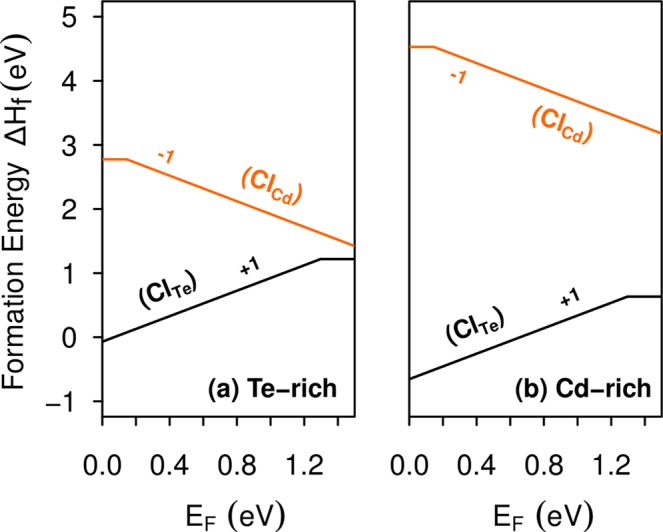
Formation energies of substitutional chlorine in CdTe, ClTe and ClCd, as a function of the Fermi level, under (a) Te-rich condition and (b) Cd-rich condition. The slopes of the formation energy lines indicate the charge states and changes in its slopes indicates defect transition states.
The ClTe-VCd complex in CdTe
The ClTe-VCd complex in CdTe is formed when a Cl atom replaces a Te atom nearest neighbor to a Cd vacancy38. Previous DFT calculations have identified the isolated Cd vacancy as the dominant intrinsic acceptor in CdTe39–41. We found that VCd is stable in Td, D2d, and C2v symmetries, being the VCd(C2v) configuration the global minimum. We also found that VCd is stable in C3v symmetry in the single-negative charge state, which is stabilized by a hole polaron, in good agreement with previous calculations41. In the neutral charge state, VCd(Td) and VCd(D2d) are 0.64 and 2.11 eV higher in energy than VCd(C2v), respectively. The VCd(C2v) structure is characterized by the formation of a Te-Te dimer between two undercoordinated Te atoms neighboring to the vacancy. Our results show that this dimer has a bond distance of 2.773 Å, while the others Te atoms remain three-fold coordinated and are displaced inward the vacancy by about 0.24 Å with respect to their perfect crystal positions. Interestingly, the VCd(C2v) in the neutral charge state exhibits a ground-state configuration with all the valence band filled and all the conduction bands empty. This result is in close agreement with recent DFT-HSE06 calculations, although the formation of the Te-Te dimer was not reported42. On the other hand, the VCd(D2d) structure reveals the formation of two Te-Te dimers with bond distances of 2.765 Å, while its electronic structure indicates a double donor character.
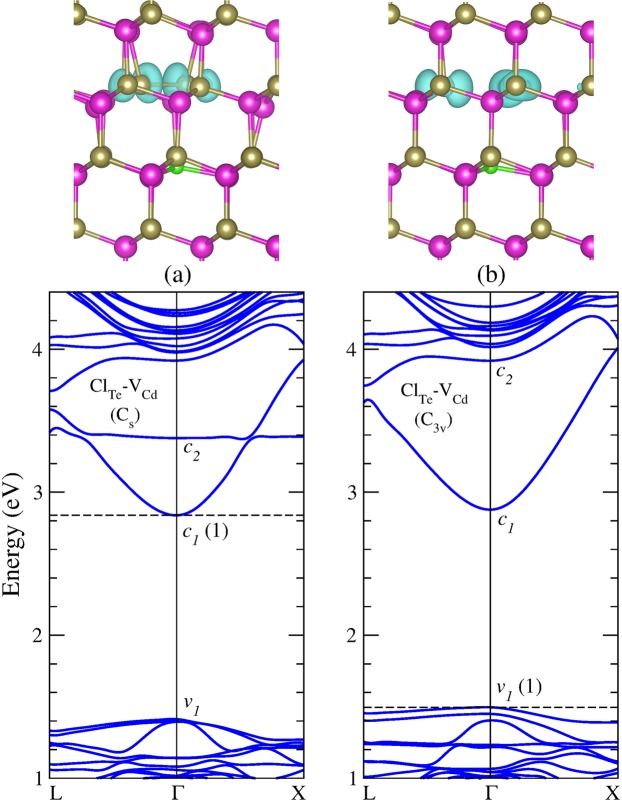
Next, we investigate the formation of the ClTe-VCd complex starting from the VCd(Td) geometry by substituting a neighboring Te atom by a Cl atom. Our results for the electronic band structure and the equilibrium geometry are shown in Fig. 3(b). We find that the neutral complex is stable in C3v symmetry [hereafter referred as (ClTe-VCd)(C3v)], where the ClTe impurity moves outward the vacancy by 0.5 Å, while the three-fold coordinated Te atoms relax inward by 0.29 Å with respect to their perfect crystal positions, as shown in Fig. 3(b). Moreover, neutral (ClTe-VCd)(C3v) has a hole at the VBM, indicating a shallow acceptor character in good agreement with previous theoretical35,43,44 and experimental32 results.
Figure 3.
Equilibrium geometry and band structure calculations of the complexes (a) (ClTe-VCd) (Cs), and (b) (ClTe-VCd)(C3v) in the neutral charge state. The dashed line indicates the Fermi energy. Charge density isosurfaces for the impurity level (c2) in (a) and the level at VBM (v1) in (b) are plotted for ρ = 0.005 e/Å3 and ρ = 0.001 e/Å3, respectively.
By taking into account the high stability of the VCd(C2v) structure that form the Te-Te dimer, we construct another complex by substituting an under-coordinated Te atom by a Cl atom. Our results for the band structure and equilibrium geometry of this complex are shown in Fig. 3(a). We find that the new complex geometry preserves the Te-Te dimer of the VCd(C2v) configuration with a bond distance of 2.771 Å. Moreover, we found that the substitutional chlorine moves outward the Cd vacancy by 0.5 Å. This complex has Cs symmetry with only one symmetry plane [hereafter referred as (ClTe-VCd)(Cs)], which is 0.73 eV higher in energy than the (ClTe-VCd)(C3v) structure in the neutral charge state. It is worth noting that the ClTe-VCd complex was recently studied by Lindström et al., using DFT-HSE06 calculations36. They found two equilibrium geometries for this complex, which is stable in both Cs and C3v symmetries, in the neutral and in the negative charge state, respectively. Although the two configurations of the complex agree with our calculations, the equilibrium geometry of the neutral (ClTe-VCd)(Cs) differs from our results. We find the formation of a Te-Te dimer, while Lindström et al.36 found only a small approach between the same Te atoms, suggesting that its configuration may be a metastable state.
Our results shows that the (ClTe-VCd)(Cs) complex has a shallow donor property, in contrast to the (ClTe-VCd)(C3v) complex, which is a shallow acceptor, as shown Fig. 3. Although with a higher formation energy, the (ClTe-VCd)(Cs) complex is likely to form in the single-positive charge state, which is a ground state configuration with all the valence band filled and all the conduction bands empty. Indeed, for the Fermi energy close to the VBM the [(ClTe-VCd)(Cs)]+ configuration has much lower energy than the [(ClTe-VCd)(C3v)]− polaronic configuration found in ref.36, which acts as a harmful electron trap.
Figure 4 shows the formation energies of (ClTe-VCd)(Cs) and (ClTe-VCd)(C3v), indicating that both complexes can coexist for the Fermi energy close to VBM + 0.33 eV, the energy at which their formation energies are equal, as indicated by the arrow. As the transition between the C3v and Cs geometries involves the formation of a Te-Te dimer, we want to know the energy needed to overcome the barrier between them, that is the activation energy, and if this process is likely to occur at the operational conditions. To do that, we calculate the minimum energy path (MEP) of neutral ClTe-VCd moving from C3v to Cs geometries, using the climbing-image nudged elastic band (NEB) method45. This method finds the MEP between two local minima previously obtained, by optimizing intermediate geometries called images. Then, the activation energy is obtained by calculating the difference between the lowest minimum and the saddle point. In our calculations we obtain the MEP using GGA-PBE functional, considering a 128-atom supercell with all atoms free to relax, and ten images between the C3v and Cs local minima. We obtain an activation energy of 0.64 eV, as shown in Fig. 5.
Figure 4.
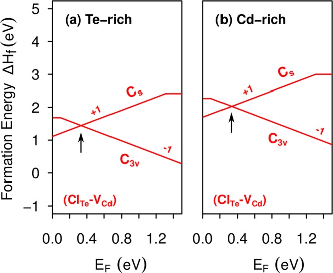
Formation energies of the ClTe-VCd complex in Cs and C3v symmetries, as a function of the Fermi level, under (a) Te-rich condition and (b) Cd-rich condition.
Figure 5.
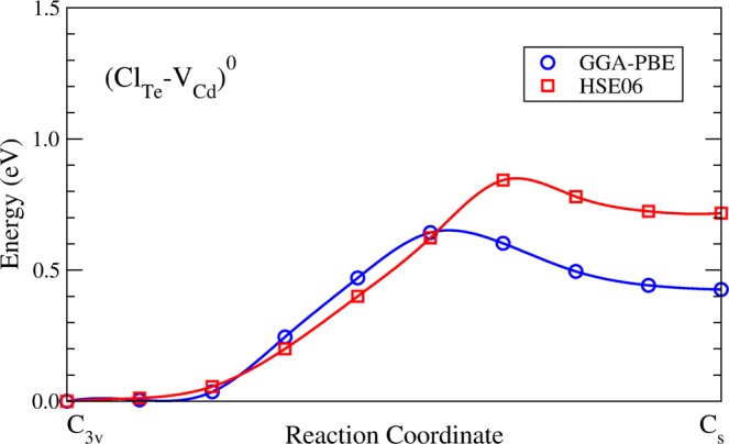
Minimum energy paths for transition of the neutral complex ClTe-VCd from C3v to Cs symmetries, as calculated with GGA-PBE and HSE06 functionals.
To estimate the MEP using the hybrid HSE06 functional, which is the functional used throughout this work, we re-evaluated the GGA-PBE images previously found using now the HSE06 functional without allow the system to relax (single-point energy). It is important to note that NEB calculations using directly the HSE06 functional are not possible due to the huge computational time required. Our results show an activation energy of 0.85 eV, as shown in Fig. 5. The difference between both minimum energy paths is partially attributed to a residual strain in the single-point calculation and the inclusion of the fraction of exact exchange due to the hybrid functional. It is interesting to note that the larger difference between MEPs is obtained when the Te-Te dimer becomes to form. We believe that a realistic activation energy for transition between the C3v and Cs geometries should be something between GGA-PBE and HSE06 calculations. Experiments have measured activation energies for the chlorine diffusion in CdTe to be of 0.63 and 1.32 eV for a temperature range between 200 and 700 °C46. Therefore, the activation energy for the C3v to Cs transition in the neutral ClTe-VCd complex lies in the range of 0.64 to 0.85 eV, suggesting that it is likely to occur.
However, the activation energy for the inverse transition Cs to C3v, which would be the most probable direction, is just of 0.15 eV. Therefore, at the HSE06 level of calculation, the formation of the ClTe-VCd complex would start with a neutral VCd vacancy with C2v geometry. If a Cl impurity occupies the position of one of the two three-fold coordinated Te atoms surrounding the vacancy, a neutral (ClTe-VCd)(Cs) complex would form. According to Fig. 3(a), this complex is a shallow donor being likely to lose an electron, changing to the (ClTe-VCd)(C3v) geometry after overcoming an energy barrier of 0.15 eV.
The 2ClTe-VCd complex in CdTe
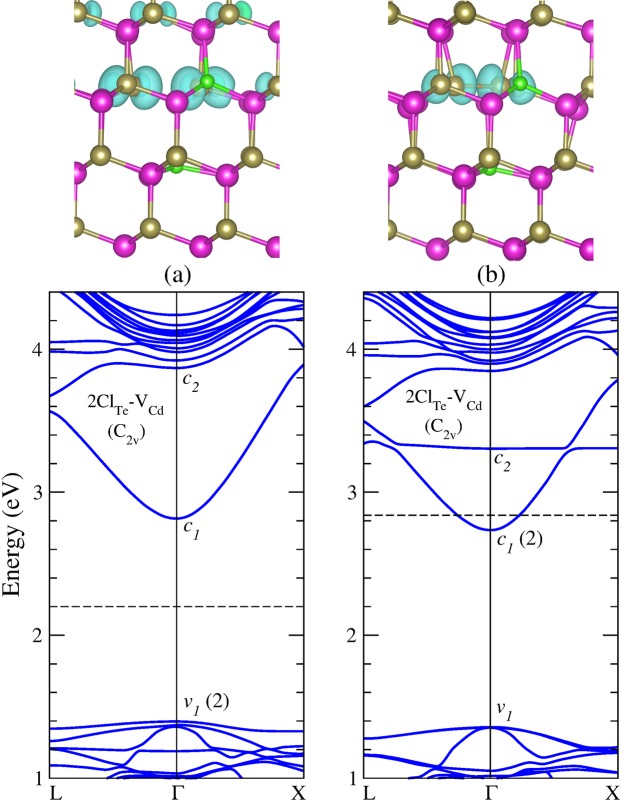
We subsequently investigate the possibility of a new complex consisting of two Cl atoms substituting two of the four undercoordinated Te atoms nearest neighbors to a Cd vacancy (hereafter referred as 2ClTe-VCd). This complex was predicted in 1974 by Canali et al.47, suggesting that it would be likely to be found in high-resistivity donor-doped CdTe. After substituting the second Te atom by a Cl atom in (ClTe-VCd)(C3v) as shown in Fig. 3(b), we observe that the system relaxes to the 2ClTe-VCd configuration shown in Fig. 6(a), exhibiting C2v symmetry. The inclusion of the second chlorine fills the hole that (ClTe-VCd)(C3v), shows at the VBM, stabilizing the (2ClTe-VCd)(C2v) complex in neutral charge state. Moreover, the electronic structure of this complex shows that the neutral charge state is a ground-state configuration, that is with all the valence bands filled and all the conduction bands empty.
Figure 6.
Equilibrium geometry and band structure calculations of the neutral 2ClTe-VCd complex in the two stable configurations (a) with Te atoms separated, and (b) with the Te atoms forming a dimer. The dashed line indicates the Fermi energy. Charge density isosurfaces for the level at the VBM (v1) in (a) and the impurity level (c2) in (b) are plotted for ρ = 0.001 e/Å3 and ρ = 0.005 e/Å3, respectively.
In addition, we find a second configuration for the 2ClTe-VCd complex, where the two adjacent undercoordinated Te atoms form a Te-Te dimer with a bond length of 2.771 Å, preserving the C2v symmetry. In the neutral charge state, this complex has two excess electrons in the conduction bands, as shown in Fig. 6(b), indicating that 2ClTe-VCd is a double donor that would tend to transfer its excess electrons to uncompensated acceptors such as the VCd. In this way, the ground-state configuration [2ClTe-VCd]2+ should be stabilized.
Figure 7 shows the calculated formation energies for the two configurations of the 2ClTe-VCd complex as a function of the Fermi level, under both Te-rich and Cd-rich growth conditions. We find that the Te-Te dimer configuration, which will be referred as (2ClTe-VCd)(d), has the lowest formation energy for the Fermi level close to the VBM (n-type CdTe), being likely to be found under this condition. Whereas for other Fermi level positions, the complex configuration with the separated Te atoms is the most stable. Thus, the crossing point of formation energy lines, indicated by arrows in Fig. 7, shows that 2ClTe-VCd introduces a shallow transition level ε(2 + /0) at VBM + 0.1 eV. Interestingly, this complex exhibits the same defect formation energies under both Te-rich and Cd-rich growth conditions.
Figure 7.
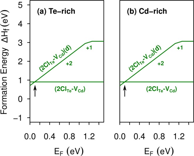
Formation energies of the 2ClTe-VCd complex as a function of the Fermi level, under (a) Te-rich condition and (b) Cd-rich condition. The neutral charge state represents the complex with separated Te atoms and the positive charge states represent the complex with a Te dimer.
The ClTe-TeCd complex in CdTe
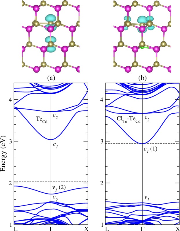
We now turn to examine the complex formed by the substitutional chlorine (ClTe) nearest neighbor to the Te antisite (TeCd). Previous DFT calculations have extensively studied the TeCd antisite because is one of the most abundant native defect under Te-rich growth conditions7,35,40,48–52. Lindström et al.52 using the hybrid functional HSE06 have reported three charge states for this defect: , , and , which are stable in Td, C3v and Cs symmetries, respectively. We found similar results, but according to our formation energy calculations only and would be stable, as shown in Fig. 8. The discrepancy can be attributed to finite size effect, as the authors of ref.52 applied a potential alignment scheme in a 128-atom supercell, in contrast to our formation energy calculations performed with a larger 250-atom supercell. It is interesting to note that TeCd shows higher formation energies than ClTe for all values of the Fermi energy in the band gap, as can be seen by comparing Figs 8 and 2, suggesting that the chlorine impurity would be energetically favorable over any native defect. Moreover, the TeCd defect exhibits a negative-U behavior, where the single-positive charge state is never stable, in agreement with previous calculations40,50,52,53. Hence, the TeCd defect shows a ε(2 + /0) transition level at VBM + 0.4 eV. However, in a previous work using accurate quasiparticle DFT + GW calculations we found this state at VBM + 1.0 eV53. The electronic structure of shows an empty t2 level in the higher part of the CdTe band gap. After capturing two electrons, the defect experiences a Jahn-Teller distortion, which is characterized by the breaking a Te-Te bond, lowering the symmetry from Td to C3v. In this way, the t2 level split into a fully-occupied a1 level and an empty e level, which are represented by v1 and c2 levels in the band structure, shown in Fig. 9(a).
Figure 8.
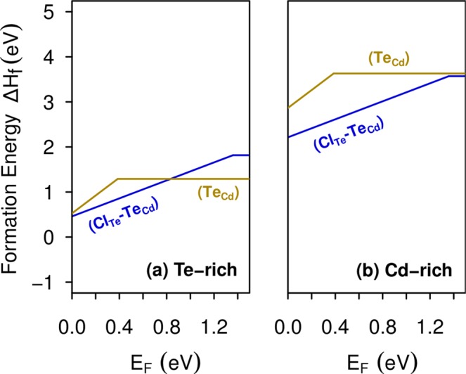
Formation energies of the TeCd antisite and the ClTe-TeCd complex as a function of the Fermi level, under (a) Te-rich condition and (b) Cd-rich condition.
Figure 9.
Equilibrium geometry and band structure calculations of (a) the TeCd antisite, and (b) the ClTe-TeCd complex, in the neutral charge state. The dashed line indicates the Fermi energy. Charge density isosurfaces of the occupied level in the band gap (v1) in (a) and the VBM level (v1) in (b) are plotted for ρ = 0.005 e/Å3 and ρ = 0.001 e/Å3, respectively.
Concerning ClTe-TeCd, our results suggests that this complex only exists in single positive charge state with similar formation energy than the TeCd antisite, as shown Fig. 8. Figure 9(b) shows the band structure calculations of this complex, indicating a shallow donor character, without exhibiting deep levels in the band gap. This result suggests the passivation of the fully-occupied a1 level of after the formation of the ClTe-TeCd complex, providing an additional explanation to the beneficial effect of the chlorine treatment as experimentally reported.
Interstitial chlorine in CdTe
In an earlier paper54, we discussed the role of interstitial chlorine in CdTe (Cli). In that study we found that Cli is stable in at least five distinct interstitial sites with close formation energies. Moreover, this impurity introduces shallow energy levels that may lead to a donor-acceptor compensation mechanism. Nevertheless, the dominant configurations of Cli have a formation energies higher than ClTe and the 2ClTe-VCd complex for values of the Fermi level near midgap, under both Te-rich and Cd-rich growth conditions. We refer the interested reader to ref.54, the work of Lindström et al.36, and the topical review of Yang et al.44.
Self-compensation in chlorine-doped CdTe
Figure 10 summarizes the formation energies Cl-related defects in CdTe, which are likley to be formed due to their low formation energies. For values of the Fermi level in the lower part of the band gap (n-type CdTe), we observe that (ClTe)+ is the most relevant defect under both Te-rich and Cd-rich growth conditions, acting as the dominant donor. Whereas, for the Fermi level in the higher part of the band gap (p-type CdTe), the relevant defect is the complex [(ClTe-VCd)(C3v)]−, which is the dominant acceptor. Therefore, in the Te-rich limit, the closed-shell (ClTe)+ donor would be compensated by the [(ClTe-VCd)(C3v)]− acceptor after transferring its electron in excess, leading to the Fermi level pinning at VBM + 0.92 eV, as indicate the arrow in Fig. 10(a).
Figure 10.
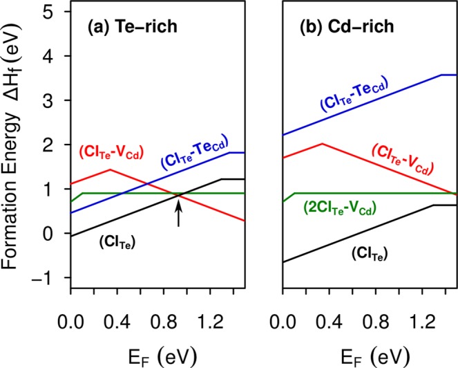
Formation energies of most stable Cl-related defects in CdTe, as a function of the Fermi level, under (a) Te-rich condition and (b) Cd-rich condition.
Interestingly, at the crossing point between (ClTe)+ and [(ClTe-VCd)(C3v)]− in Te-rich CdTe, the complex 2ClTe-VCd is only 0.05 eV higher in energy [see Fig. 10(a)]. Thus, the existence of 2ClTe-VCd complexes will contribute to stabilize the charge neutrality condition, allowing the Fermi level pinning in CdTe:Cl without introducing a compensating deep level at variance of the cases of CdTe:Sn27 and CdTe:Ge55. These results are in good agreement with the earlier work of Höschl et al.56, who suggested that ClTe-VCd and 2ClTe-VCd dominate (59% and 40%) over Cd vacancies as compensating acceptors in semi-insulating CdTe:Cl. Moreover, Lindström et al.36 also suggested the possible formation of a tricomplex consisting of two Cl ions and one Cd vacancy. An alternative explanation for the deep level observed by spectroscopy methods34 could be the possible formation of chlorine complexes with Te antisites, which are the dominant recombination centers in CdTe53. However, our results for the ClTe-TeCd complex do not show any deep levels in the band gap. In addition, our calculations show that ClTe is the dominant defect in the Cd-rich limit for any value of the Fermi energy, suggesting that chlorine can be used as an effective n-type dopant under these conditions. For instance, the incorporation of Cl under controlled Cd partial pressures might help to populate the intermediate band in CdTe:Sn27.
Summary
In summary, we have investigated the electronic structure, formation energies, and transition states of substitutional chlorine ClTe and ClCd, and the complexes formed by ClTe with the most probable defects found in Te-rich CdTe, namely the Cd vacancy and the Te antisite. We find that the ClTe-VCd complex can exist in two geometries, with Cs and C3v symmetries, showing shallow donor and acceptor properties, respectively. We also identify a second complex containing two substitutional chlorine neighboring to the cadmium vacancy 2ClTe-VCd, which also can exist in two geometries, both with C2v symmetry. The latter is found stable only in double positive charge state for n-type CdTe, while the former exhibits a ground-state configuration. Concerning the ClTe-TeCd complex, our results suggest that it is stable only in single positive charge state with similar formation energy than the TeCd antisite. For a Fermi energy close to the middle of the CdTe band gap, the three complexes show formation energies of around 1 eV under Te-rich condition, as shown in Fig. 10(a), suggesting that they are equally likely to be found. Table 1 compares the formation energy values for all the Cl-related defects studied under Te-rich and Cd-rich conditions for the Fermi energy at the VBM.
Table 1.
Formation energy (in eV) of the Cl-related defects in CdTe under study. The Fermi energy is set at the valence band maximum. Lower values for the formation energy, in general less than 1 eV, indicates the most likely defects to be found.
| Defect | ΔHf (Te rich) | ΔHf (Cd rich) |
|---|---|---|
| (ClTe)1+ | −0.07 | −0.65 |
| (ClTe)0 | 1.22 | 0.63 |
| (ClCd)1− | 2.92 | 4.68 |
| (ClCd)0 | 2.82 | 4.57 |
| [(ClTe-VCd) (Cs)]1+ | 1.11 | 1.70 |
| [(ClTe-VCd) (Cs)]0 | 2.42 | 3.00 |
| [(ClTe-VCd) (C3v)]1− | 1.78 | 2.36 |
| [(ClTe-VCd) (C3v)]0 | 1.68 | 2.27 |
| [(2ClTe-VCd) (d)]2+ | 0.71 | 0.71 |
| [(2ClTe-VCd) (d)]1+ | 1.81 | 1.81 |
| [(2ClTe-VCd) (d)]0 | 3.06 | 3.06 |
| [(2ClTe-VCd)]0 | 0.90 | 0.90 |
| (TeCd)2+ | 0.53 | 2.87 |
| (TeCd)0 | 1.29 | 3.63 |
| (ClTe-TeCd)1+ | 0.46 | 2.21 |
| (ClTe-TeCd)0 | 1.82 | 3.57 |
Finally, we find that neither the complexes under study nor the substitutional Cl impurity induce deep level in the CdTe band gap. Therefore, our calculations suggest that self compensation between Cl-induced shallow donors and acceptors should be responsible for the high resistivity observed in detector-grade CdTe:Cl, usually grown in a Te-rich environment, in agreement with previous hypothesis35. Particularly, the (ClTe)+ shallow donor would be compensated by the [(ClTe-VCd)(C3v)]− shallow acceptor, leading to the Fermi level pinning at VBM + 0.92 eV. In addition, our results show that the formation of the ClTe-TeCd complex passivates the deep level associated to the Te antisite (TeCd), confirming to some extent the beneficial effect of chlorine in CdTe.
Methods
We performed first-principles calculations based on the density functional theory (DFT)57,58, as implemented in the Vienna Ab Initio Simulation Package (VASP)59. We used the Heyd-Scuseria-Ernzerhof (HSE06)60,61 hybrid functional with the standard mixing parameter α = 25%, a plane-wave basis set with a cutoff energy of 285 eV. The core-valence interaction is described by the projector augmented-wave mathod62. Our calculations were performed using large 250-atom supercells, which were fully relaxed until the forces on each atom were less than 0.025 eV/Å. Our computational approach improves previous theoretical works in which smaller 64-atom supercell were used36,44,63, despite the fact that the convergence of hybrid functionals with respect to the supercell size may be slower than its local and semi-local counterparts15,64,65. Additionally, due to the high computational cost of the HSE06 calculations, only the Γ point was used for the Brillouin zone sampling, whereas band structures calculations were performed using a 128-atom supercell.
The formation energy (ΔHf) of a defect in charge state q can be written as a function of the Fermi level (EF) and the chemical potentials of the atomic species (μi) as follows66:
| 1 |
where Etot[Xq] and Etot[bulk] are the total energy of the system with a defect in charge state q and the pristine system, respectively. EVBM is the energy of the valence band maximum. ni is the number of atoms of type i that have added or removed from a pristine system. For instance, in the case of Cl substituting a Cd atom in the charge state q, the formation energy can be obtained as:
| 2 |
where Etot(CdnTen) is the total energy of a supercell containing n primitive cells of CdTe and Etot(Cdn−1TenCl)q is the energy of the same supercell with one Cd atom replaced by a Cl atom with q electrons removed. For Cl substituting a Te atom in charge state q (), the same procedure is applied, just exchanging Te by Cd in Eq. (2).
The chemical potentials in Eq. (2) are defined as:
| 3 |
where EX is the energy per atom of bulk-phase Cd and Te, and gas-phase Cl (Cl2). In addition, the thermodynamic equilibrium requires the following restrictions to the chemical potentials:
| 4 |
| 5 |
| 6 |
Inequalities (4) and (5) represent necessary conditions to avoid that elements and compounds segregate, whereas ΔμCd = 0 and ΔμTe = 0 represent Cd-rich and Te-rich conditions, respectively. ΔH(CdCl2) and ΔH(CdTe) are the heats of formation of CdCl2 and CdTe. The numerical values of heats of formation are obtained from HSE06 calculations. Relations (4) and (6) impose that both ΔμCd and ΔμTe are larger than ΔH(CdTe). Others expressions like (5) can be set to avoid the formation of other compounds like TeCl4 and Te3Cl2, but in practice (5) sets the maximum possible value for ΔμCl in equilibrium with CdTe. Etot(CdnTenCl)q in Eq. (2) includes size corrections for electrostatic interactions between nearest-neighbor images in the supercell calculation67. No additional corrections for band filling are needed67, as we used only the Γ point for the Brillouin zone sampling.
Acknowledgements
This work was supported by CONICYT/FONDECYT under Grants No. 1170480 (W.O.) and No. 1171807 (E.M-P.). Powered@NLHPC: This research was partially supported by the supercomputing infrastructure of the NLHPC (ECM-02).
Author Contributions
The research and manuscript were led by authors W.O. and M.A.F.; W.O. conducted the band structure calculations and created Figures 1, 3, 5, 6, and 9; E.M.P. and M.A.F. conducted the formation energy calculations; M.A.F. created Figures 2, 4, 7, 8, and 10. All authors analysed the results and reviewed the manuscript.
Competing Interests
The authors declare no competing interests.
Footnotes
Publisher’s note: Springer Nature remains neutral with regard to jurisdictional claims in published maps and institutional affiliations.
References
- 1.Loferski JJ. Theoretical considerations governing the choice of the optimum semiconductor for photovoltaic solar energy conversion. J. Appl. Phys. 1956;27:777–784. doi: 10.1063/1.1722483. [DOI] [Google Scholar]
- 2.Green MA. Third generation photovoltaics: Ultra-high conversion efficiency at low cost. Prog. Photovolt: Res. Appl. 2001;9:123–135. doi: 10.1002/pip.360. [DOI] [Google Scholar]
- 3.Bosio A, Rosa G, Romeo N. Past, present and future of the thin film CdTe/CdS solar cells. Solar Energy. 2018;175:31–43. doi: 10.1016/j.solener.2018.01.018. [DOI] [Google Scholar]
- 4.Szeles C. CdZnTe and CdTe materials for X-ray and gamma-ray radiation detector applications. Phys. Status Solidi B. 2004;241:783–790. doi: 10.1002/pssb.200304296. [DOI] [Google Scholar]
- 5.Richter M, Siffert P. High resolution gamma ray spectroscopy with CdTe detector systems. Nucl. Instrum. Methods Phys. Res. A. 1992;322:529–537. doi: 10.1016/0168-9002(92)91227-Z. [DOI] [Google Scholar]
- 6.Del Sordo S, et al. Progress in the development of CdTe and CdZnTe semiconductor radiation detectors for astrophysical and medical applications. Sensors. 2009;9:3491–3526. doi: 10.3390/s90503491. [DOI] [PMC free article] [PubMed] [Google Scholar]
- 7.Carvalho A, Öberg S, Briddon P. Intrinsic defect complexes in CdTe and ZnTe. Thin Solid Films. 2011;519:7468–7471. doi: 10.1016/j.tsf.2010.12.128. [DOI] [Google Scholar]
- 8.Scheiber C, Giakos GC. Medical applications of CdTe and CdZnTe detectors. Nucl. Instrum. Methods Phys. Res. A. 2001;458:12–25. doi: 10.1016/S0168-9002(00)01032-9. [DOI] [Google Scholar]
- 9.Green MA, et al. Solar cell efficiency tables (version 53) Prog. Photovoltaics Res. Appl. 2019;27:3–12. doi: 10.1002/pip.3102. [DOI] [Google Scholar]
- 10.Chander S, Dhaka M. CdCl2 treatment concentration evolution of physical properties correlation with surface morphology of CdTe thin films for solar cells. Mater. Res. Bull. 2018;97:128–135. doi: 10.1016/j.materresbull.2017.08.038. [DOI] [Google Scholar]
- 11.Lindström A, Mirbt S, Sanyal B, Klintenberg M. High resistivity in undoped CdTe: carrier compensation of Te antisites and Cd vacancies. J. Phys. D. 2015;49:035101. doi: 10.1088/0022-3727/49/3/035101. [DOI] [Google Scholar]
- 12.Cola A, Farella I, Pousset J, Valletta A. On the relation between deep level compensation, resistivity and electric field in semi-insulating CdTe: Cl radiation detectors. Semicond. Sci. Technol. 2016;31:12LT01. doi: 10.1088/0268-1242/31/12/12LT01. [DOI] [Google Scholar]
- 13.Mandel G. Self-compensation limited conductivity in binary semiconductors. i. theory. Phys. Rev. 1964;134:A1073–A1079. doi: 10.1103/PhysRev.134.A1073. [DOI] [Google Scholar]
- 14.Yang J-H, Yin W-J, Park J-S, Wei S-H. Self-regulation of charged defect compensation and formation energy pinning in semiconductors. Sci Rep. 2015;5:16977. doi: 10.1038/srep16977. [DOI] [PMC free article] [PubMed] [Google Scholar]
- 15.Flores MA, Orellana W, Menéndez-Proupin E. Self-compensation in phosphorus-doped CdTe. Phys. Rev. B. 2017;96:134115. doi: 10.1103/PhysRevB.96.134115. [DOI] [Google Scholar]
- 16.Walsh A, Zunger A. Instilling defect tolerance in new compounds. Nat. Mater. 2017;16:964. doi: 10.1038/nmat4973. [DOI] [PubMed] [Google Scholar]
- 17.Li C, et al. Review. Nature. 2018;29:20718–20725. doi: 10.1007/s10854-018-0212-9. [DOI] [Google Scholar]
- 18.Panchuk O, et al. Iv group dopant compensation effect in CdTe. J. Crystal Growth. 1999;197:607–611. doi: 10.1016/S0022-0248(98)00798-2. [DOI] [Google Scholar]
- 19.Flores MA. Defect properties of Sn-and Ge-doped ZnTe: suitability for intermediate-band solar cells. Semicond. Sci. Technol. 2018;33:015004. doi: 10.1088/1361-6641/aa9a8b. [DOI] [Google Scholar]
- 20.Ablekim T, et al. Self-compensation in arsenic doping of CdTe. Sci. Rep. 2017;7:4563. doi: 10.1038/s41598-017-04719-0. [DOI] [PMC free article] [PubMed] [Google Scholar]
- 21.Guo D, Brinkman D, Shaik AR, Ringhofer C, Vasileska D. Metastability and reliability of CdTe solar cells. J. Phys. D: Appl. Phys. 2018;51:153002. doi: 10.1088/1361-6463/aab1e1. [DOI] [Google Scholar]
- 22.Colegrove E, et al. Experimental and theoretical comparison of Sb, As, and P diffusion mechanisms and doping in CdTe. J. Phys. D: Appl. Phys. 2018;51:075102. doi: 10.1088/1361-6463/aaa67e. [DOI] [Google Scholar]
- 23.McCandless BE, et al. Overcoming carrier concentration limits in polycrystalline CdTe thin films with in situ doping. Sci. Rep. 2018;8:14519. doi: 10.1038/s41598-018-32746-y. [DOI] [PMC free article] [PubMed] [Google Scholar]
- 24.Gorlei P, Parfenyuk O, Ilashchuk M, Nikolaevich I. Doping of cadmium telluride with germanium, tin, and lead. Inorg. Mater. 2005;41:1266–1269. doi: 10.1007/s10789-005-0298-3. [DOI] [Google Scholar]
- 25.Babentsov V, et al. Dependence of the Sn 0/2+ charge state on the fermi level in semi-insulating CdTe. J. Mater. Sci. 2007;22:3249–3254. doi: 10.1557/JMR.2007.0404. [DOI] [Google Scholar]
- 26.Babentsov V, Franc J, Fauler A, Fiederle M, James R. Doping, compensation, and photosensitivity of detector grade CdTe. J. Mater. Res. 2008;23:1751–1757. doi: 10.1557/JMR.2008.0198. [DOI] [Google Scholar]
- 27.Flores MA, Menéndez-Proupin E, Orellana W, Peña JL. Sn-doped CdTe as promising intermediate-band photovoltaic material. J. Phys. D: Appl. Phys. 2017;50:035501. doi: 10.1088/1361-6463/50/3/035501. [DOI] [Google Scholar]
- 28.Shockley W, Read WT. Statistics of the recombinations of holes and electrons. Phys. Rev. 1952;87:835–842. doi: 10.1103/PhysRev.87.835. [DOI] [Google Scholar]
- 29.Hall RN. Electron-hole recombination in germanium. Phys. Rev. 1952;87:387–387. doi: 10.1103/PhysRev.87.387. [DOI] [Google Scholar]
- 30.Ohmori M, Iwase Y, Ohno R. High quality CdTe and its application to radiation detectors. Mater. Sci. Eng. B. 1993;16:283–290. doi: 10.1016/0921-5107(93)90061-Q. [DOI] [Google Scholar]
- 31.Popovych V, et al. The effect of chlorine doping concentration on the quality of CdTe single crystals grown by the modified physical vapor transport method. J. Crystal Growth. 2007;308:63–70. doi: 10.1016/j.jcrysgro.2007.07.041. [DOI] [Google Scholar]
- 32.Seto S, Tanaka A, Masa Y, Kawashima M. Chlorine-related photoluminescence lines in high-resistivity cl-doped CdTe. J. Cryst. Growth. 1992;117:271–275. doi: 10.1016/0022-0248(92)90758-B. [DOI] [Google Scholar]
- 33.Pavlyuk M, Subbotin I, Kanevsky V, Artemov V. Stepwise cooling technique as a method of growing high-perfection cl-compensated CdTe. J. Cryst. Growth. 2017;457:112–116. doi: 10.1016/j.jcrysgro.2016.06.046. [DOI] [Google Scholar]
- 34.Pousset J, Farella I, Gambino S, Cola A. Subgap time of flight: A spectroscopic study of deep levels in semi-insulating CdTe:Cl. J. Appl. Phys. 2016;119:105701. doi: 10.1063/1.4943262. [DOI] [Google Scholar]
- 35.Biswas K, Du M-H. What causes high resistivity in CdTe. New J. Phys. 2012;14:063020. doi: 10.1088/1367-2630/14/6/063020. [DOI] [Google Scholar]
- 36.Lindström A, Klintenberg M, Sanyal B, Mirbt S. Cl-doping of Te-rich CdTe: Complex formation, self-compensation and self-purification from first principles. AIP Advances. 2015;5:087101. doi: 10.1063/1.4928189. [DOI] [Google Scholar]
- 37.Krasikov D, Knizhnik A, Potapkin B, Sommerer T. Why shallow defect levels alone do not cause high resistivity in CdTe. Semicond. Sci. Technol. 2013;28:125019. doi: 10.1088/0268-1242/28/12/125019. [DOI] [Google Scholar]
- 38.Hofmann DM, et al. Identification of the chlorine a center in CdTe. Phys. Rev. B. 1992;45:6247–6250. doi: 10.1103/PhysRevB.45.6247. [DOI] [PubMed] [Google Scholar]
- 39.Wei S-H, Zhang SB. Chemical trends of defect formation and doping limit in II–VI semiconductors: The case of CdTe. Phys. Rev. B. 2002;66:155211. doi: 10.1103/PhysRevB.66.155211. [DOI] [Google Scholar]
- 40.Du M-H, Takenaka H, Singh DJ. Native defects and oxygen and hydrogen-related defect complexes in CdTe: Density functional calculations. J. Appl. Phys. 2008;104:093521. doi: 10.1063/1.3000562. [DOI] [Google Scholar]
- 41.Shepidchenko A, Sanyal B, Klintenberg M, Mirbt S. Small hole polaron in CdTe: Cd-vacancy revisited. Sci. Rep. 2015;5:14509. doi: 10.1038/srep14509. [DOI] [PMC free article] [PubMed] [Google Scholar]
- 42.Yang J-H, Shi L, Wang L-W, Wei S-H. Non-radiative carrier recombination enhanced by two-level process: a first-principles study. Sci. Rep. 2016;6:21712. doi: 10.1038/srep21712. [DOI] [PMC free article] [PubMed] [Google Scholar]
- 43.Zhu H, Gu M, Huang L, Wang J, Wu X. Structural and electronic properties of CdTe:Cl from first-principles. Mater. Chem. Phys. 2014;143:637–641. doi: 10.1016/j.matchemphys.2013.09.046. [DOI] [Google Scholar]
- 44.Yang J-H, Yin W-J, Park J-S, Metzger W, Wei S-H. First-principles study of roles of Cu and Cl in polycrystalline CdTe. J. Appl. Phys. 2016;119:045104. doi: 10.1063/1.4940722. [DOI] [Google Scholar]
- 45.Henkelman G, Uberuaga B, Jónsson H. A climbing image nudged elastic band method for finding saddle points and minimum energy paths. J. Chem. Phys. 2000;113:9901. doi: 10.1063/1.1329672. [DOI] [Google Scholar]
- 46.Jones ED, Malzbender J, Mullins JB, Shaw N. The diffusion of Cl into CdTe. J. Phys.: Condens. Matter. 1994;6:7499–7504. doi: 10.1088/0953-8984/6/37/005. [DOI] [Google Scholar]
- 47.Canali C, Ottaviani G, Bell R, Wald F. Self-compensation in CdTe. J. Phys. Chem. Solids. 1974;35:1405–1413. doi: 10.1016/S0022-3697(74)80246-5. [DOI] [Google Scholar]
- 48.Berding MA. Native defects in CdTe. Phys. Rev. B. 1999;60:8943. doi: 10.1103/PhysRevB.60.8943. [DOI] [Google Scholar]
- 49.Wei S-H, Zhang SB, Zunger A. First-principles calculation of band offsets, optical bowings, and defects in cds, cdse, CdTe, and their alloys. J. Appl. Phys. 2000;87:1308. doi: 10.1063/1.372014. [DOI] [Google Scholar]
- 50.Lordi V. Point defects in Cd(Zn)Te and TlBr: Theory. J. Cryst. Growth. 2013;379:84–92. doi: 10.1016/j.jcrysgro.2013.03.003. [DOI] [Google Scholar]
- 51.Shepidchenko A, Mirbt S, Sanyal B, Håkansson A, Klintenberg M. Tailoring of defect levels by deformations: Te-antisite in CdTe. J. Phys.: Condens. Matter. 2013;25:415801. doi: 10.1088/0953-8984/25/41/415801. [DOI] [PubMed] [Google Scholar]
- 52.Lindström A, Mirbt S, Sanyal B, Klintenberg M. High resistivity in undoped CdTe: Carrier compensation of Te antisites and Cd vacancies. J. Phys. D: Appl. Phys. 2016;49:035101. doi: 10.1088/0022-3727/49/3/035101. [DOI] [Google Scholar]
- 53.Flores MA, Orellana W, Menéndez-Proupin E. First-principles DFT + GW study of the Te antisite in CdTe. Comput. Mater. Sci. 2016;125:176–182. doi: 10.1016/j.commatsci.2016.08.044. [DOI] [Google Scholar]
- 54.Orellana Walter, Menéndez-Proupin Eduardo, Flores Mauricio A. Energetics and Electronic Properties of Interstitial Chlorine in CdTe. physica status solidi (b) 2018;256(3):1800219. doi: 10.1002/pssb.201800219. [DOI] [Google Scholar]
- 55.Scharager C, Siefert P, Höschl P, Moravec P, Vaněček M. Characterization of germanium-doped CdTe crystals. Phys. Status Solidi A. 1981;66:87–92. doi: 10.1002/pssa.2210660108. [DOI] [Google Scholar]
- 56.Höschl P, Grill R, Franc J, Moravec P, Belas E. Native defect equilibrium in semi-insulating CdTe(Cl) Mater. Sci. Eng. B. 1993;16:215–218. doi: 10.1016/0921-5107(93)90047-Q. [DOI] [Google Scholar]
- 57.Kohn W, Sham LJ. Self-consistent equations including exchange and correlation effects. Phys. Rev. 1965;140:A1133–A1138. doi: 10.1103/PhysRev.140.A1133. [DOI] [Google Scholar]
- 58.Kohn W. Nobel lecture: Electronic structure of matter—wave functions and density functionals. Rev. Mod. Phys. 1999;71:1253. doi: 10.1103/RevModPhys.71.1253. [DOI] [Google Scholar]
- 59.Kresse G, Furthmüller J. Efficient iterative schemes for ab initio total-energy calculations using a plane-wave basis set. Phys. Rev. B. 1996;54:11169–11186. doi: 10.1103/PhysRevB.54.11169. [DOI] [PubMed] [Google Scholar]
- 60.Heyd J, Scuseria GE, Ernzerhof M. Hybrid functionals based on a screened coulomb potential. J. Chem. Phys. 2003;118:8207–8215. doi: 10.1063/1.1564060. [DOI] [Google Scholar]
- 61.Heyd J, Scuseria GE, Ernzerhof M. Erratum: “hybrid functionals based on a screened coulomb potential” [j. chem. phys. 118, 8207 (2003)] J. Chem. Phys. 2006;124:219906. doi: 10.1063/1.2204597. [DOI] [Google Scholar]
- 62.Blöchl PE. Projector augmented-wave method. Phys. Rev. B. 1994;50:17953–17979. doi: 10.1103/PhysRevB.50.17953. [DOI] [PubMed] [Google Scholar]
- 63.Pan J, Metzger WK, Lany S. Spin-orbit coupling effects on predicting defect properties with hybrid functionals: A case study in CdTe. Phys. Rev. B. 2018;98:054108. doi: 10.1103/PhysRevB.98.054108. [DOI] [Google Scholar]
- 64.Bang J, et al. Difficulty in predicting shallow defects with hybrid functionals: Implication of the long-range exchange interaction. Phys. Rev. B. 2013;88:035134. doi: 10.1103/PhysRevB.88.035134. [DOI] [Google Scholar]
- 65.Flores MA, Orellana W, Menéndez-Proupin E. Accuracy of the Heyd-Scuseria-Ernzerhof hybrid functional to describe many-electron interactions and charge localization in semiconductors. Phys. Rev. B. 2018;98:155131. doi: 10.1103/PhysRevB.98.155131. [DOI] [Google Scholar]
- 66.Freysoldt C, et al. First-principles calculations for point defects in solids. Rev. Mod. Phys. 2014;86:253–305. doi: 10.1103/RevModPhys.86.253. [DOI] [Google Scholar]
- 67.Lany S, Zunger A. Assessment of correction methods for the band-gap problem and for finite-size effects in supercell defect calculations: Case studies for ZnO and GaAs. Phys. Rev. B. 2008;78:235104. doi: 10.1103/PhysRevB.78.235104. [DOI] [Google Scholar]


