Abstract
Although the number of total knee replacement (TKR) surgeries is growing rapidly, functionality and pain-reduction outcomes remain unsatisfactory for many patients. Continual monitoring of knee loads after surgery offers the potential to improve surgical procedures and implant designs. The goal of this study is to characterize a triboelectric energy harvester under body loads and to design compatible frontend electronics to digitize the load data. The harvester prototype would be placed between the tibial component and polyethylene bearing of a TKR implant. The harvester generates power from the compressive load. To examine the harvester output and the feasibility of powering a digitization circuitry, a triboelectric energy harvester prototype is fabricated and tested. An axial tibiofemoral load profile from normal walking (gait) is approximated as a 1 Hz sine wave signal and is applied to the harvester. Because the root mean square of voltages generated via this phenomenon is proportional to the applied load, the device can be simultaneously employed for energy harvesting and load sensing. With an approximated knee cyclic load of 2.3 kN at 1 Hz, the harvester generated output voltage of 18 V RMS, and an average power of 6 μW at the optimal resistance of 58MΩ. The harvested signal is rectified through a negative voltage converter rectifier and regulated through a linear-dropout regulator with a combined efficiency of 71%. The output of the regulator is used to charge a supercapacitor. The energy stored in the supercapacitor is used for low resolution sensing of the load through a peak detector and analog-to-digital converter. According to our analysis, sensing the load several times a day is feasible by relying only on harvested power. The results found from this work demonstrate that triboelectric energy harvesting is a promising technique for self-powering load sensors inside knee implants.
1. Introduction
Activities of daily living such as walking, running, and jumping result in the transfer of significant loads through the human knee joint [1]. An epidemic of osteoarthritis and associated cartilage degeneration, even in young and active patients, has increased total knee replacement surgeries that use prosthetic components. Although most patients are satisfied with the outcomes of these surgeries, approximately 20% are not satisfied with the resulting levels of functionality and pain after surgery [2]. A major contributor to poor functioning TKRs is incorrect ligament balancing[3], which can accelerate wear from joint reaction force imbalances and promote prosthetic loosening [4]. While there are various techniques to analyze the kinematics of TKRs after surgery, the loads experienced by these devices are challenging to measure, and the loads can eventually lead to implant failure.
To obtain more information about the functionality of the knee within and after the surgery, different implanted TKRs are proposed in the literature. In 2006, the first sensor is embedded in a TKR for a senior, male patient by D’Lima et al. [5,6]. The implanted TKR sensor consists of four load cells with a wireless micro-transmitter. However, the major limitation of their design is the power source where a coil system was placed around the knee. This method may affect the accuracy of the collected data. Later, extensive in vivo studies were reported on measuring the loading of the knee joints during activities of daily living by the Bergmann group [7–9]. They provided complete details about the forces and moments acting on the knee joints. However, the major drawback of their work was that the reported data was measured for a specific implant design and cannot be transferred directly to other implants or the natural human knee.
The use of sensors for intra-and post-operative guidance has created much enthusiasm in biomedical research in recent years, particularly in the field of orthopedics. Such intra-operative sensors are available commercially for the total knee replacements. However, they only are useful to provide data in the operating room and should be removed by the end of the surgery [10–12], and therefore the post-operative measurements are missing. Because the required in vivo information consists of gathering force measurements during and after surgery, recent studies investigated sensors that can measure the knee loads and use them to harvest energy [13–17].
A common mechanism proposed for a self-powering load sensor is piezoelectric transduction. Piezoelectric energy harvesters generate a voltage from deformations. Platt et al. [14] investigated the benefits of piezoelectric ceramics in total knee replacement applications. They found that piezoelectric power generation is a promising technique for in vivo sensors and embedded MEMS devices. Almuuahed et al. [13] investigated four self-powered knee-load sensors using piezoelectric transducers placed between the tibial tray and a polyethylene bearing. The design can detect the knee forces and harvest energy up to 5 mW under normal walking activity. In a recent study, Safaei et al. [17] presented an optimized design and embedded the piezoelectric sensor in the polyethylene bearing, which is considered preferable and more suitable with traditional and FDA-approved tibial components. However, piezoelectric ceramics are brittle, limiting the strain they can withstand. Flexible piezoelectric materials have been made but they have lower piezoelectric constants.Other transducers such as electromagnetic mechanisms have been proposed for knee implants by Luciano et al. [18]. They used coils on the tibial plate and magnets on the femoral insert to convert their relative rotations to electricity. The limitation of their proposed design is that it may not be easily incorporated into a variety of implant designs and can affect the strength of the implant.
In recent years, a triboelectric mechanism has been demonstrated as an alternative method for mechanical energy harvesting [19–21]. Compared with other harvester types such as piezoelectric or electromagnetic, the greatest energy density is obtained with the triboelectric transducer. The triboelectric transduction mechanism has the advantages of simple fabrication, excellent reliability, high efficiency, and low cost. In the triboelectric mechanism, contact electrification happens when two different materials at different polarities come into contact with each other and then separate for a small gap [22–27]. The small separation needed between triboelectric materials to generate power means the device can be packaged to allow a suitable amount of deformation in an embedded sensor. The gap, usually in a range of 10–300 microns, can be tuned to maximize the amount of energy harvested. The cyclic process leads to the flow of charges between the two triboelectric layers and alternating current is produced. The harvester output voltage RMS is proportional to the load because larger forces cause the generator’s two layers to become more deeply engaged and more charges are generated, leading to larger output voltage. This proportionality and the large compressive loads available at the knee make triboelectric generators an appropriate mechanism to harvest energy.
Previously reported attempts at harvesting energy in TKR implants to power telemetry circuitry have employed piezoelectric and electromagnetic power generation, and share the common limitations mentioned above. The feasibility of the triboelectric mechanism for pressure sensor application was first investigated by Fan et al [28]. The sensor was studied for ultra-low pressure ranges such as those induced by dropping a feather. In this study, we are investigating the feasibility of the triboelectric mechanism to act as a sensor under the high pressures that happen at the knee implant. We propose a triboelectric energy-harvesting load measurement system that can be installed between the Ultra-High-Molecular-Weight Polyethylene (UHMWPE) bearing insert and the tibial tray of TKR implants, allowing the load measurement to be incorporated into any TKR system. Triboelectric power generation in TKR implants has never been demonstrated, therefore this paper focuses on the development and experimental characterization of a prototype device at physiologically relevant load magnitudes and frequencies.
2. MATERIALS AND METHODS
2.1. Triboelectric Generator Configuration
A schematic for the triboelectric generator is shown in Fig. 1. The harvester is composed of two major parts separated with rubber springs: an upper Aluminum part and a lower PDMS part bound to a bottom Aluminum layer. The device operates based on the periodic contact and separation between upper and lower parts. The required separation is small, within a range of less than 300 microns. The upper Al part is a used as a mold with micropatterns. The lower part is made from a thin Aluminum substrate glued to a polydimethylsiloxane (PDMS) layer. The PDMS layer is fabricated using the upper Aluminum as a mold, and the two layers have reverse micropatterns. This PDMS material is considered biocompatible and used widely for implantable devices applications [29]. When a cyclic axial force is applied to the generator, the rubber springs will be compressed and then the upper and lower parts undergo a continuous contacting and separating motion. This contact and separation mechanism between the two surfaces with micro-patterns spurs charges to be generated. The more force the larger the output will be. This feature enables the triboelectric generator to be an effective energy harvesting mechanism at the knee joint.
Figure 1:
Schematic of the triboelectric energy harvester configuration
2.2. Triboelectric Transducer Fabrication Process
The fabrication process for the PDMS layer depends on the upper AL mold. This mold is designed and made by Progressive Tools [30] with dimensions of (5.2 × 3.7 × 0.4) cm. The harvester area is 19.24 cm2 and is as large as the usable area of a typical tibial tray in knee implants. Our mold is designed with semi-cylindrical grooves, as shown in Fig. 2a, to increase the surface contact between the two layers. First, the top Al mold is immersed in distilled water and placed in an ultrasonication machine for 10 minutes. Then the process is repeated twice with acetone and water, respectively. After that the Al is dried with Nitrogen. A 10 : 1 mixture of a silicone elastomer base and a curing agent is made to form the PDMS layer. The mixture is placed in a vacuum chamber at −17 PSI until all air bubbles are removed from the mixture. After that, the mold and a square piece of glass are treated with SIH5841.0 material in a vacuum chamber for half an hour. This treatment helps in peeling the PDMS layer from the Al mold after baking. The PDMS mixture is poured on the glass, and immediately the molds are placed over the PDMS mixture and pressed slowly at an angle to reduce the air bubbles in the final PDMS layer. The glass with the mixture and Al mold is placed on a heater and baked at 80oC for an hour. After baking, the PDMS layer is peeled from the Al mold yielding a 320 μm thick PDMS layer, with a semi-cylindrical reverse pattern, as shown in Fig. 2b. To create the lower electrode, a thin Al layer is spin coated with a thin layer of the PDMS mixture and baked for an hour at 80oC. Then, the Al layer is plasma treated and bonded to the PDMS layer.
Figure 2:
Upper and lower layers of the triboelectric generator (a) Aluminum mold.(b) SEM image for PDMS layer.
2.3. Working Mechanism
The working principle of the triboelectric mechanism is depicted in Fig. 3. Initially, the two layers are separated and are without charge, as depicted in Fig. 3a. When the device is subject to a compression load at the knee, the two layers contact each other, as shown in Fig. 3b. The Al layer donates electrons to the PDMS layer. Therefore, on the contact, the Al layer gets positively charged while the PDMS layer gets negatively charged. The PDMS layer induces electrostatic charge at the bottom AL layer. When the mechanical load is released, the mechanical restoring force from the rubber springs separates the two layers. At this stage, if the Al layers are connected, the potential difference between them forces the current to flow from the upper Al layer to the lower Al layer, see Fig. 3c. This current keeps flowing until the two layers are fully separated and reach an equilibrium where the triboelectric charges and electrostatic charges are equalized, as illustrated in Fig 3d. With continued cyclic loading, the two layers start to approach each other, and capacitance is charged. The charged capacitance and charged electrode cause a current flow in the opposite direction from the lower Al layer to the upper layer, as shown in Fig. 3e. The cyclical reversal of electron flows mean the device produces an alternating current.
Figure 3:
Operating mechanism for the triboelectric energy harvester.
2.4. Instrumented TKR with a triboelectric generator
Figure 4 shows the proposed schematic for the instrumented TKR. TKR consists of the femoral, tibial tray, and the UHMWPE bearing parts. For optimal load measurements, the triboelectric generators are placed between the tibial tray and the UHMWPE bearing. Because the backs of the tibial tray and the UHMWPE bearing are flat, we simplify the analysis by placing our generator between two flat surfaces and test it with an MTS machine to investigate the performance. For future work, the generators will be placed in a TKR implant and be tested in a VIVO [Advanced Mechanical Technology, Inc., Watertown, MA] joint simulator.
Figure 4:
Schematic for the total knee replacement.
2.5. Experimental Setup
The goal of this experiment is to test the generator under normal walking activity. Body loads are Fx and Fy, which act act in lateral and anterior directions, respectively, and the axial force component, Fz, which always acts in the direction of the implant shaft. For walking and jogging, the highest force component was found to be the axial force, Fz, which is almost equal to the total force [9]. In this test, the axial force profile is approximated as a sine-wave signal at 1 Hz. The experimental setup used to evaluate the performance of the triboelectric generator is shown in Fig. 5. The setup consists of an MTS 858 Servo Hydraulic Test System with FlexTest SE Controller. The MTS is responsible for conducting a cyclic axial load, while the amplitude is tuned with the FlexTest controller. The MTS has a built-in load cell to measure the applied force on the generator.
Figure 5:
Schematic of the experimental setup.
The generated voltage signal from the triboelectric generator is measured using a Keithley 6514 and an ExceLINX program. The Keithley 6514 has an internal impedance of 200 TΩ to ensure the voltage measurements of the harvester are not compromised by the resistance of the measurement instrument. The experimental test is repeated at different external resistances connected to the harvester to obtain the optimal resistance where a maximum power can be achieved. A variable resistance box is used to control the resistance.
3. RESULTS AND DISCUSSIONS
3.1. Energy Harvesting Analysis
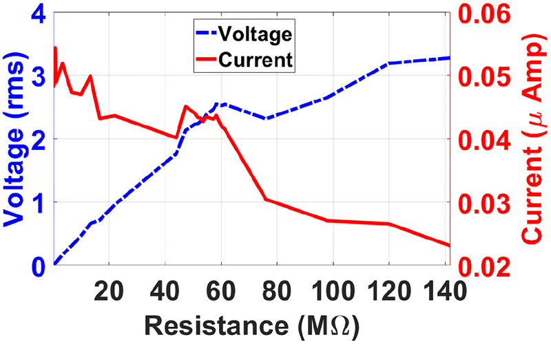
To characterize the electric output of the triboelectric generator, the short-circuit current (Isc) was measured under different periodic compressive forces of 200 N, 500 N, and 1000 N applied by the MTS machine at a constant frequency of 1 Hz as shown in Figure 6. By increasing the applied load, a higher current can be achieved. However, our interest in this study is the instantaneous current because of the presence of frontend electronics. To extract the maximum power, we identify the internal resistance of the harvester and match it with the circuit resistance. The internal resistance is referred to as the optimal resistance. To estimate the optimal resistance for the triboelectric energy harvester, the testing was conducted at a specific cyclic load with a force of 100 N with varied external resistance up to 142 MΩ. The variations of the voltage and current outputs with the external resistance load are shown in Fig. 7. The voltage and current curves intersect at the optimal resistance of R = 58 MΩ. The corresponding average power outputs of the harvester with the external load resistance are shown in Fig. 8. The optimal resistance from the power curve is obtained at 58 MΩ, which matches the result from the intersection of the voltage and current outputs in Fig. 7. In addition, a maximum average power of 0.125 μW is generated at this optimal resistance. The load of 100 N is significantly below the typical knee loads, which are more than 2000 N. This testing was only conducted to estimate the internal resistance of the device.
Figure 6:
The variation of the short-circuit current output for three different loads at 1 Hz frequency.
Figure 7:
The variation of the voltage and current as a function of resistance.
Figure 8:
The variation of the average power as a function of resistance.
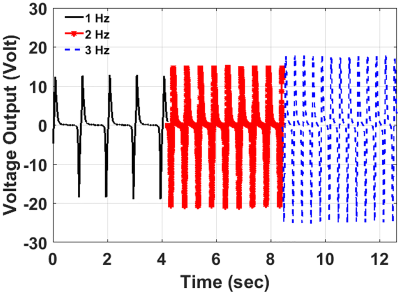
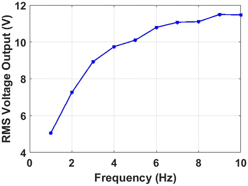
Forcing frequency affects the harvester output. Fig. 9 shows the output voltages of the triboelectric generator under three different frequencies, 1, 2, and 3 Hz. The voltages clearly increase with faster frequencies. At high frequencies, because there is more contact in a certain amount of time, more charges accumulate, resulting in higher voltages. The variation of the root mean square of the generated output voltage with a wider range of frequencies is shown in Fig. 10. The output voltage increases rapidly up to 6 Hz where the increases slow down and stabilize at approximately 11.4 V.
Figure 9:
The variation of the voltage output for three different frequencies. Greater voltage is generated by increasing the frequency.
Figure 10:
The variation of the root mean square of the voltage output with the frequency.
Next, the performance of the generator is explored under different cyclic loading. The main goal of this test is to evaluate the harvester output under equivalent TKR loads to design a suitable load data processing unit (Section 4). The generated voltages for 100 N, 500 N and 2,300 N are shown in Fig. 11. The results show the output voltage increases with the applied cyclic load. This increase in the output voltage can be correlated to the larger surface area of contact. With an applied force of 2300 N, which is equivalent to the load from walking of an average weighted person, at the optimal load resistance of 58 MΩ, the harvester generates a 100 V peak-to-peak (18 V RMS) and a 6 μW of average power. Based on the results from Fig. 11, the output voltage is not linearly proportional to the applied force. The applied force is a sinusoidal wave, while the output voltage is not sinusoidal, and this difference is related to the nonlinear mechanism of triboelectric charge generation [21]. However, the root mean square of the voltage is proportional to the load (Fig. 12). The root mean square of the harvester analog signal can be easily obtained in the frontend electronic circuit and be related to the load amount. Fig. 12 shows the RMS of the voltage output of the triboelectric generator under different applied cyclic loads up to 3300 N and 1 Hz frequency at the optimal resistance extracted before. The RMS voltage outputs are proportional to the load applied, where greater voltage can be generated with more applied force. The reason for this can be related to the surface area of contact between the generator layers. The triboelectric principle relies on the contact and separation of the generator layers (PDMS and Al) both at the macro and micro-scales. Because micro-patterns exist in both layers, higher applied loads cause larger penetration into the PDMS layer leading to an increase in the triboelectric charges generated on the surface and thus higher output voltage. With a maximum applied load of 3300 N, the triboelectric harvester generates an RMS voltage of 23 V at the output.
Figure 11:
The time domain output voltage signals at three different applied axial loads. High peak-to-peak voltage is generated by increasing the applied force. The cyclic load is applied at R = 58MΩ and 1 Hz frequency.
Figure 12:
The RMS output voltage at different applied axial loads. Greater voltage is generated by increasing the applied force. The cyclic load is applied at R = 58MΩ and 1 Hz frequency.
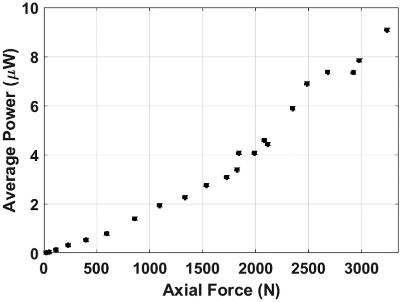
The corresponding average power generated under the same axial loading are shown in Fig. 13. The maximum average power generated is found to be 9.5 μW at a maximum applied load of 3300 N. This relationship between the applied force and the voltage and power outputs is considered promising for powering load sensors and their telemetry circuitry for TKR applications. Next, we design and evaluate the performance of a frontend electronic circuit that can use the harvested energy to digitize the load data.
Figure 13:
The average generated power for different applied axial loads. The cyclic load is applied at R = 58MΩ and 1 Hz frequency.
4. FRONTEND ELECTRONICS FOR THE TRIBOELECTIC HARVESTER
The proposed frontend electronic system for the triboelectric harvester designed for a knee implant is shown in Fig.14. The frontend electronics consist of a rectifier, a low dropout regulator, a supercapacitor, a power management block, a delta-sigma analog-to-digital converter (ADC), and a low complexity microcontroller with telemetry. An electrical model is generated for the triboelectric harvester discussed above. This electrical model produces an output AC signal similar to the actual harvester. This AC signal is then fed into the CMOS rectifier to convert it to a DC voltage. This DC voltage is further passed through a regulator to obtain a stabilized and a regulated voltage that is sufficiently insensitive to variations in the current and supply voltage. This regulated output charges a supercapacitor to store the energy. Once sufficient energy is stored, as determined by the power management block, the supercapacitor starts to get discharged through the ADC and microcontroller to further process the harvested signal and store the output. Specifically, the harvested voltage signal and the supercapacitor output voltage are fed into a delta-sigma ADC to get the digital bit stream. The digital data is stored in the microcontroller nonvolatile memory. When sufficient data is stored, the energy stored within the supercapacitor is used to wirelessly transmit the data. The supercapacitor is 0.1 F with a maximum voltage of 0.9 V. Thus when fully charged, it can store 40.5 mJ energy, which is sufficient for wireless transmission. Note that the power management circuitry power gates the microcontroller during standby mode, thereby preventing the subthreshold leakage.
Figure 14:
Block diagram of the triboelectric system
4.1. Electrical Model of the Harvester
The electrical model of the triboelectric harvester that provides the required input power, as well as the signal to monitor, is described in this section. The behavior of the harvester is characterized by using Equations (1) and (2) [31],
| (1) |
| (2) |
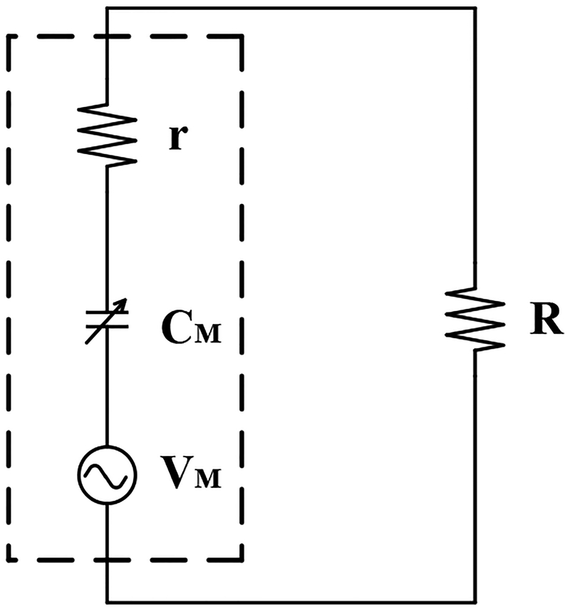
In Equation (1), the three terms on the right-hand side can be modeled using three circuit elements, a voltage source VM, a variable capacitance CM and an internal resistance r. The capacitive term originates from the capacitance between the two electrodes of the harvester, the voltage term arises because of the separation of the polarized tribocharges, and the resistance term models the impedance of the voltage source. The electrical model can be represented by a serial connection of these three circuit elements, as shown in Fig. 15.
Figure 15:
Electrical model of the triboelectric harvester.
The electrical model is connected to an external load resistance R based on Equation (2). Increasing the velocity of motion increases the frequency of AC voltage source VM, which in turn decreases the matched resistance. The tribocharge density does not affect the matched load resistance. From basic thermodynamics theory, VM and CM depend only on the moving distance (x) and structural parameters and not on motion parameters such as velocity and acceleration. Using the finite element method (FEM) and continuous fractional interpolation, a VM-x and CM-x relationship for a contact-mode triboelectric harvester has been generated [32–34],
| (3) |
| (4) |
where σ is the triboelectric surface charge density, ϵ0 is the permittivity of free space, S is area of dielectrics in the harvester and d0 is the effective dielectric thickness. The values of these physical and electrical parameters based on the designed harvester are listed, respectively, in Table 1 and Table 2.
Table 1:
Physical parameters used to generate the electrical model.
| Parameter | Symbol | Value |
|---|---|---|
| Dielectric 1 | ϵr1 | 2.4 |
| Thickness of Dielectric 1 | d1 | 320 μm |
| Dielectric 2 | ϵr2 | Metal |
| Thickness of Dielectric 2 | d1 | 0 μm |
| Effective dielectric thickness | d0 = d1 / ϵr1 + d2 / ϵr2 | 133 μm |
| Width of dielectrics | w | 5.2 cm |
| Length of dielectrics | l | 3.7 cm |
| Area of dielectrics | S = w × l | 19.24 cm2 |
| Separation distance | x | 0.5 mm – 1 mm |
| Tribo-charge surface density | σ | 100 μCm−2 |
| Internal Resistance | r | 57 mΩ |
| External load resistance | R | 58.3 MΩ |
Table 2:
Parameters of the electrical model.
| Parameter | Symbol | Value |
|---|---|---|
| Internal resistance | r | 57 MΩ |
| External load resistance | R | 58.3 MΩ |
| Model capacitance | CM | 40 pF – 100 pF |
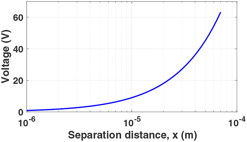
Based on these values, SPICE simulations of the electrical model have been performed. The relationship between output voltage and the separation distance x is depicted in Figure 16. The voltage increases with the distance x between the dielectrics.
Figure 16:
Voltage output of the model as a function of separation distance x
The transient output voltage produced by the electrical model is compared with the measured output voltage of the harvester in Figure 17. The output currents are also compared in Figure 18. As demonstrated by these figures, the model can represent the harvester with sufficient accuracy. Note that as the distance between the plates of the harvester changes, the harvester impedance also changes. These harvester dynamics are accounted for in the model using a variable capacitance CM that depends upon the separation distance x. Thus, the input impedance of the model dynamically varies.
Figure 17:
Comparison of model and harvester output voltages
Figure 18:
Comparison of model and harvester output currents.
According to these results, a maximum voltage of 17.95 V and a maximum input power of 6.09 μW is generated by the model at the matched optimal resistance, which represents the measured harvested power accurately. Note that the input impedance of the electrical circuitry is approximately 37.2 MΩ at 1 Hz. Since the optimal resistance is 58.3 MΩ, the delivered power to the circuit is reduced from 6.09 μW to 4.46 μW. The input impedance is relatively large due to sufficiently low frequency of 1 Hz. This power is used for the entire electronic frontend circuitry, as described in the following sections.
4.2. Rectifier
The harvested AC signal is converted into a DC voltage of approximately 1.2 V through a negative voltage converter rectifier (NVC) [35], as shown in Figure 19.
Figure 19:
A Negative Voltage Converter (NVC) rectifier
Due to the full gate cross-coupled topology, an NVC rectifier performs the rectification process with a high efficiency. During the positive input cycle, when the input voltage is less than the threshold voltage (Vac < Vth), neither of the transistors conducts and no current flows through the circuit. When the input voltage becomes greater than the threshold voltage (Vac > Vth), transistors MP1 and MP2 provide a current path to the output. The operation is similar during the negative cycle where the transistors MN1 and MN2 provide the current path.
The NVC rectifier achieves high power efficiency when the load is purely resistive. The efficiency, however, is reduced when a reactive element is added to the load due to the reverse current induced from output to the input port. This current flows due to the bidirectional MOSFET characteristic and stored charge within the capacitive load, where the output voltage is higher than the input voltage. The NVC rectifier provides a low sensitivity to input voltage variations and is widely used in low voltage, high-efficiency energy harvesters.
4.3. LDO Regulator
A low dropout (LDO) regulator, as shown in Fig. 20 converts the input DC voltage into a regulated voltage of desired value within a specified tolerance range while compensating for variations in the output current.
Figure 20:
A low-dropout (LDO) regulator
The LDO consists of a voltage reference circuit for producing the voltage Vref, an error amplifier EA that produces an output voltage proportional to the difference between the reference and output voltages, a pMOS power transistor MP to deliver the required current to output, resistive divider to determine voltage conversion ratio, and an output capacitor CL to ensure stability.
The error amplifier consists of a differential input stage followed with a common source output stage, producing a DC gain of approximately 70 dB. The high gain ensures a high-resolution error signal at the output. The phase margin is 57.81°, ensuring a stable operation.
Reducing the dropout voltage and quiescent current increases the power efficiency of the LDO. Hence, the power transistor is sized sufficiently large to lower the dropout voltage and quiescent current of the regulator, while permitting the flow of the required large current to the load. Furthermore, diode-connected nMOS transistors, MN1, MN2, MN3 and MN4, are used (instead of resistors) to further enhance the efficiency and reduce physical area. These transistors are sized to achieve the desired voltage conversion ratio of 0.75. Thus, the unregulated input voltage of 1.2 V is converted into a regulated voltage of 0.9 V.
It is important to note that the proposed LDO is free from any external bias voltage, making it applicable to energy harvesting implantable applications.
4.4. Delta-Sigma ADC
The output of the triboelectric harvester is used not only as the power source but also as the data signal that is digitized to monitor loads. The delta-sigma ADC is highly suitable for biomedical implants and energy harvesting applications due to low complexity, low power, and small area. Irrespective of the number of bits, a delta-sigma ADC consists of only one integrator and comparator, as shown in Fig. 21.
Figure 21:
Block diagram of the Delta-Sigma ADC
The analog input voltage Vin is first differentiated from the output of 1-bit digital-to-analog converter (DAC) using a switched capacitor circuit. An integrator then adds the output of the differentiator to the value it has stored from the previous integration step. The output of the integrator is then fed into a comparator, which compares the output with voltage Vmid. It outputs a logic 1 if the integrator output is greater than or equal to Vmid, otherwise, it produces a logic 0. A 1 bit DAC feeds the output of the comparator to the differentiator through a feedback loop. The output of the comparator then goes through a D flip-flop to produce the final digital bit stream [36]. The schematic diagram of the designed ADC is shown in Figure 22.
Figure 22:
Schematic of the Delta-Sigma ADC
The voltages VH, Vmid, and VL are, respectively, 0.9 V, 0.6 V, and 0.3 V. The capacitors C1 and C2 are kept at 100 fF. The two non-overlapping clocks ϕ1 and ϕ2 run at 50 kHz to reduce power consumption and ensure correct functioning of the triboelectric knee implant. The reset and reset2 signals have the same frequency, as determined by,
| (5) |
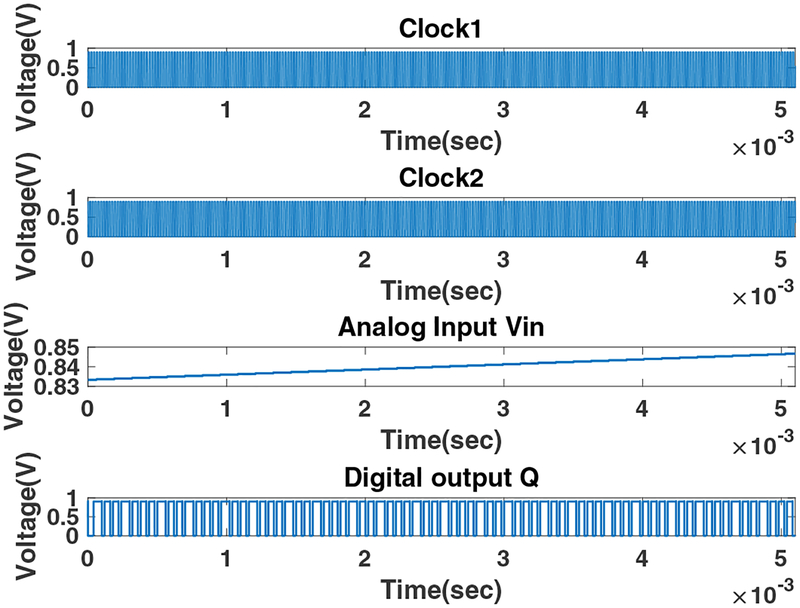
where fclk is the clock frequency, fR is the reset and reset2 frequency and N is the number of bits. In the designed ADC, N is equal to 8, and the reset and reset2 frequencies are 195 Hz. The signals Vϕ2 and are produced using a CMOS NAND gate and an inverter. The clock signals, analog input voltage, and digital output voltage obtained from the ADC are shown in Figure 23. To check the accuracy of the ADC, the analog and digital figures of merit, represented, respectively, by Equations (6) and (7), are calculated. The percentage error between the two should be minimized.
Figure 23:
Digital bit stream from the ADC
| (6) |
| (7) |
For example, for an input voltage of 0.84 V, the analog FOM is 0.90 and from the digital bit stream, the digital FOM is 0.88. The percentage error between the two is only 2.22%. The figures of merits were calculated for various input voltages (ranging from −57.05 V to 58.97 V) and the average percentage error is approximately 5.75%, demonstrating that the designed ADC is sufficiently accurate to digitize the sensed gait signals.
The power efficiencies of the designed NVC rectifier and LDO regulator are listed in Table 3.
Table 3:
Efficiencies of the NVC rectifier and LDO regulator.
| Circuit | Input and Output | Load | η (%) |
|---|---|---|---|
| NVC Rectifier | AC signal from the model converted to 1.2 V DC | LDO regulator | 72.24 |
| LDO Regulator | 1.2 V DC from the rectifier converted to 0.9 V DC | Delta-Sigma ADC | 69.55 |
The overall power consumed by the rectifier, regulator and ADC circuits is 4.46 μW. Thus, it is possible to achieve a self-powered digitization circuitry by relying on the triboelectric energy harvester.
5. FUTURE WORK
The future work entails testing the setup under simulated Activities of daily living (ADL) profiles in vivo joint simulator for more accurate measurements. Furthermore, we will work on the integration of supercapacitor and a low complexity microcontroller into the proposed triboelectric system. These units are needed for wireless transmission of the digitized data that corresponds to the sensed load. There will also be an emphasis on further reducing the overall power consumption by producing a lower DC voltage and operating in the near/subthreshold region.
6. CONCLUSIONS
In this paper, a triboelectric energy harvester with power management and digitization circuitry for TKR applications is presented. The system uses a triboelectric generator to convert mechanical energy from an applied axial load to electrical energy that can power the frontend electronic circuit. The proposed energy harvester consists of two layers with different tendencies to lose and gain electrons. The harvester has the ability to generate a voltage signal based on the triboelectric effect when it undergoes a cyclic loading from activities of daily living. An axial load is applied using an MTS servo-hydraulic load frame, to simulate the axial load passing through the knee while walking. The variation of the voltage, current, and average power with the load resistance are explored and an optimal resistance for maximum outputs is found to be 58 MΩ. In addition, the variation of the output voltages with varying frequencies is examined, where the output increases with the frequency but stabilizes above the frequency of 6 Hz. Greater outputs are obtained by increasing the applied force. The triboelectric harvester generated an average power of 6μW under an equivalent gait load of 2.3 KN at the frequency of 1 Hz, while the load digitization and harvesting circuitry are predicted to consume 4.46 μW. These preliminary results support that triboelectric power generation is a viable technique for harvesting energy to power load sensing devices for TKR applications.
ACKNOWLEDGMENT
This research has been supported by the National Institute of Arthritis and Musculoskeletal and Skin Diseases of the National Institute of Health under award number R21AR068572. The content is solely the responsibility of the authors and does not necessarily represent the official views of the National Institute of Health. The authors greatly appreciate Progressive Tool Company that made the patterned Aluminum molds.
References
- [1].Erdemir A, McLean S, Herzog W and van den Bogert AJ 2007. Clinical biomechanics 22 131–154 [DOI] [PubMed] [Google Scholar]
- [2].Bourne RB, Chesworth BM, Davis AM, Mahomed NN and Charron KD 2010. Clinical Orthopaedics and Related Research® 468 57–63 [DOI] [PMC free article] [PubMed] [Google Scholar]
- [3].Sharkey PF, Lichstein PM, Shen C, Tokarski AT and Parvizi J 2014. The Journal of arthroplasty 29 1774–1778 [DOI] [PubMed] [Google Scholar]
- [4].Dorr LD and Boiardo RA 1986. Clinical orthopaedics and related research 5–11 [PubMed] [Google Scholar]
- [5].D’Lima DD, Patil S, Steklov N, Slamin JE and Colwell CW 2006. The Journal of arthroplasty 21 255–262 [DOI] [PubMed] [Google Scholar]
- [6].DLima DD, Patil S, Steklov N, Chien S and Colwell CW 2007. Journal of biomechanics 40 S11–S17 [DOI] [PubMed] [Google Scholar]
- [7].Kutzner I, Heinlein B, Graichen F, Bender A, Rohlmann A, Halder A, Beier A and Bergmann G 2010. Journal of biomechanics 43 2164–2173 [DOI] [PubMed] [Google Scholar]
- [8].Kutzner I, Trepczynski A, Heller MO and Bergmann G 2013. PLoS One 8 e81036. [DOI] [PMC free article] [PubMed] [Google Scholar]
- [9].Bergmann G, Bender A, Graichen F, Dymke J, Rohlmann A, Trepczynski A, Heller MO and Kutzner I 2014. PloS one 9 e86035. [DOI] [PMC free article] [PubMed] [Google Scholar]
- [10].Meneghini RM, Ziemba-Davis MM, Lovro LR, Ireland PH and Damer BM 2016. The Journal of arthroplasty 31 2181–2187 [DOI] [PubMed] [Google Scholar]
- [11].Gustke KA, Golladay GJ, Roche MW, Elson LC and Anderson CR 2014. The Journal of arthroplasty 29 955–960 [DOI] [PubMed] [Google Scholar]
- [12].Roche M, Elson L and Anderson C 2014. Orthopedic Clinics 45 157–165 [DOI] [PubMed] [Google Scholar]
- [13].Almouahed S, Hamitouche C, Stindel E and Roux C 2013. Optimization of an instrumented knee implant prototype according to in-vivo use requirements Point-of-Care Healthcare Technologies (PHT), 2013 IEEE (IEEE; ) pp 5–8 [Google Scholar]
- [14].Platt SR, Farritor S, Garvin K and Haider H 2005. IEEE/ASME transactions on mechatronics 10 455–461 [Google Scholar]
- [15].Platt SR, Farritor S and Haider H 2005. IEEE/ASME transactions on Mechatronics 10 240–252 [Google Scholar]
- [16].Wilson BE, Meneghini M and Anton SR 2015. Embedded piezoelectrics for sensing and energy harvesting in total knee replacement units Active and Passive Smart Structures and Integrated Systems 2015 vol 9431 (International Society for Optics and Photonics; ) p 94311E [Google Scholar]
- [17].Safaei M, Meneghini RM and Anton SR 2018. IEEE/ASME Transactions on Mechatronics [DOI] [PMC free article] [PubMed] [Google Scholar]
- [18].Luciano V, Sardini E, Serpelloni M and Baronio G 2012. Analysis of an electromechanical generator implanted in a human total knee prosthesis Sensors Applications Symposium (SAS), 2012 IEEE (IEEE; ) pp 1–5 [Google Scholar]
- [19].Fan FR, Tian ZQ and Wang ZL 2012. Nano Energy 1 328–334 [Google Scholar]
- [20].Wang ZL 2013. ACS nano 7 9533–9557 [DOI] [PubMed] [Google Scholar]
- [21].Ibrahim A, Ramini A and Towfighian S 2018. Journal of Sound and Vibration 416 111–124 [Google Scholar]
- [22].Zi Y, Wang J, Wang S, Li S, Wen Z, Guo H and Wang ZL 2016. Nature communications 7 [DOI] [PMC free article] [PubMed] [Google Scholar]
- [23].Wang X, Niu S, Yin Y, Yi F, You Z and Wang ZL 2015. Advanced Energy Materials 5 [Google Scholar]
- [24].Yi F, Lin L, Niu S, Yang PK, Wang Z, Chen J, Zhou Y, Zi Y, Wang J, Liao Q et al. 2015. Advanced Functional Materials 25 3688–3696 [Google Scholar]
- [25].Zhou T, Zhang C, Han CB, Fan FR, Tang W and Wang ZL 2014. ACS applied materials & interfaces 6 14695–14701 [DOI] [PubMed] [Google Scholar]
- [26].Zeng W, Tao XM, Chen S, Shang S, Chan HLW and Choy SH 2013. Energy & Environmental Science 6 2631–2638 [Google Scholar]
- [27].Zhang XS, Han MD, Wang RX, Meng B, Zhu FY, Sun XM, Hu W, Wang W, Li ZH and Zhang HX 2014. Nano Energy 4 123–131 [Google Scholar]
- [28].Fan FR, Lin L, Zhu G, Wu W, Zhang R and Wang ZL 2012. Nano letters 12 3109–3114 [DOI] [PubMed] [Google Scholar]
- [29].Bélanger MC and Marois Y 2001. Journal of Biomedical Materials Research Part A 58 467–477 [DOI] [PubMed] [Google Scholar]
- [30].Progressive Tool Co kernel description. [2015-09-30]; http://www.progressivetool.com/ accessed:
- [31].Niu S, Zhou YS, Wang S, Liu Y, Lin L, Bando Y and Wang ZL 2014. Nano Energy 8 150–156 [Google Scholar]
- [32].Niu S, Wang S, Lin L, Liu Y, Zhou YS, Hu Y and Wang ZL 2013. Energy & Environmental Science 6 3576–3583 [Google Scholar]
- [33].Niu S, Liu Y, Wang S, Lin L, Zhou YS, Hu Y and Wang ZL 2014. Advanced Functional Materials 24 3332–3340 [Google Scholar]
- [34].Niu S, Wang S, Liu Y, Zhou YS, Lin L, Hu Y, Pradel KC and Wang ZL 2014. Energy & Environmental Science 7 2339–2349 [Google Scholar]
- [35].Gomez-Casseres EA, Arbulú SM, Franco RJ, Contreras R and Martínez J 2016. Comparison of passive rectifier circuits for energy harvesting applications Electrical and Computer Engineering (CCECE), 2016 IEEE Canadian Conference on (IEEE; ) pp 1–6 [Google Scholar]
- [36].Pavan S, Schreier R and Temes GC 2017. Understanding delta-sigma data converters (John Wiley & Sons; ) [Google Scholar]


