Abstract
Photon pair sources are fundamental building blocks for quantum entanglement and quantum communication. Recent studies in silicon photonics have documented promising characteristics for photon pair sources within the telecommunications band, including sub-milliwatt optical pump power, high spectral brightness, and high photon purity. However, most quantum systems suitable for local operations, such as storage and computation, support optical transitions in the visible or short near-infrared bands. In comparison to telecommunications wavelengths, the significantly higher optical attenuation in silica at such wavelengths limits the length scale over which optical-fiber-based quantum communication between such local nodes can take place. One approach to connect such systems over fiber is through a photon pair source that can bridge the visible and telecom bands, but an appropriate source, which should produce narrow-band photon pairs with a high signal-to-noise ratio, has not yet been developed. Here, we demonstrate an on-chip visible-telecom photon pair source for the first time, using high quality factor silicon nitride microresonators to generate bright photon pairs with an unprecedented coincidence-to-accidental ratio (CAR) up to (3.8 ± 0.2) × 103. We further demonstrate dispersion engineering of the microresonators to enable the connection of different species of trapped atoms/ions, defect centers, and quantum dots to the telecommunications bands for future quantum communication systems.
Long-distance quantum communication requires resources for the low-loss storage and transmission of quantum information1,2. For fiber optic networks, this presents a challenge, in that many systems that are best suited for storage, including trapped ions, neutral atoms, and spins in crystals, are connected to photons in the visible or short near-infrared (NIR) bands3, where losses in silica fibers are dominated by scattering and are orders of magnitude higher than at telecommunications wavelengths4. While a quantum frequency conversion interface can bridge the spectral gap between the relevant wavelengths5, it can be quite challenging, both in finding appropriate laser source(s) to match the input and output wavelengths, and also in limiting added noise photons due to the strong classical pump fields. These challenges are more acute as the local quantum system’s operating wavelength decreases and moves further away from the telecommunications band.
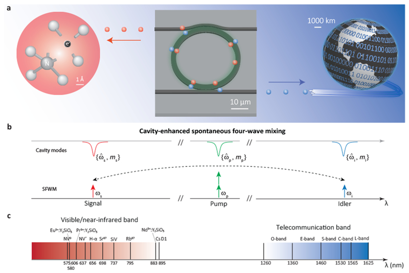
A second approach to connecting photonic quantum systems is through suitably-engineered entangled photon pair sources. In particular, quantum memories can be remotely entangled via entanglement swapping6,7, in which photons entangled with the two distant memories propagate towards each other and meet, where they are subjected to a Bell-state measurement. For visible/short-NIR memories, the propagation distance in optical fiber is limited as described above. To overcome this limitation, one can introduce entangled photon pair sources in which one photon is resonant with the memory (i.e., at a visible wavelength), and the other is in the telecom band (Fig. 1). Successive entanglement swapping operations can then entangle the memories, with their separation now limited by the propagation distance in optical fiber in the telecom. Such visible-telecom pair sources might also find use in related scenarios, for example, Bell inequality violations using nitrogen vacancy center spins in diamond8.
FIG. 1: Motivation and Scheme.
a, Intended application of this work, where photon pairs generated from a silicon nitride nanophotonic chip are used to connect visible and telecommunication bands, to enable a connection between a nitrogen vacancy center in diamond and the telecom fiber network, for example, b, Scheme for cavity-enhanced spontaneous four-wave mixing (SFWM). The continuous wave, classical pump held at frequency ωp generates signal and idler photons at ωs and ωi. respectively, dictated by energy conservation 2ωp = ωs + ωi. The nearest relevant cavity mode frequencies are at , , and , respectively. Phase-matching of light generated in these optical modes is equivalent to a condition on the cavity azimuthal mode numbers m, such that 2mp = ms + mi. c, Examples of local quantum systems with optical transitions in the visible/short near-infrared band (left), and classification of the telecommunications wavelength bands (right).
Existing visible-telecom photon pair sources are in platforms such as periodically-poled nonlinear crystals9, photonic crystal fibers10, and millimeter-scale crystalline microresonators11. The first two platforms generate broadband photons, which would require extra spectral filtering to achieve the narrow bandwidths needed for interaction with local quantum systems, and would come at the price of a decrease in collection efficiency and signal-to-noise ratio. The photon pairs from the last platform have a coincidence-to-accidental ratio (CAR) value below 20, which can be a constraint in applications. Moreover, such crystalline resonators lack the potential for scalable fabrication and integration common to the planar systems commonly used in nanophotonics.
A nanophotonic device platform for narrow-linewidth, high-quality visible-telecom photon pairs is the whispering gallery mode microresonator based on silicon photonics12. Recent studies have documented promising characteristics for photon pair sources based on spontaneous four-wave mixing (SFWM) in the telecommunications band, including submilliwatt optical pump power, high spectral brightness, and high photon purity13–18. While silicon’s narrow bandgap forbids operation below 1.1 μm, stoichiometric silicon nitride (Si3N4) has a much wider bandgap, enabling operation across wavelengths from the near-UV to the mid-infrared. Such broadband performance has been exploited in octave-spanning optical frequency combs19–21, and in the context of integrated quantum photonics, efficient single-photon-level frequency conversion interfaces between the 980 nm and 1550 nm bands22. Here, we demonstrate a family of visible/short NIR-telecom photon pair sources using the Si3N4 microresonator platform. In particular, we show that it is possible to overcome the primary challenge in the development of such sources, which is in achieving phase- and frequency-matching of narrow-band modes over a spectral separation of >250 THz. Our source produces photons at 668 nm and 1548 nm, with a photon pair flux of (7.0 ± 0.8) × 105 counts per second and a CAR of (44 ± 3) at 0.46 mW input power. The CAR increases to (3800 ± 200) at a pair flux of (1.2 ± 0.3) × 103 counts per second. Moreover, we experimentally show that the visible photons can be shifted from 630 nm to 810 nm by varying the pump wavelength and microring width. Our demonstration of a chip-integrated visible-telecom photon pair source emitting bright, pure, and narrow linewidth photons has the potential to serve as an important resource in connecting quantum memories with telecommunication networks.
System Design
The device is a Si3N4 microring resonator with a lower silicon dioxide (SiO2) cladding and a top air cladding. Si3N4 microrings support high quality factor (Q) whispering-gallery modes, which combine a long photon life-time with localization into a small effective volume (V). This leads to a large optical intensity (i.e., I ~ Q/V), which is critical for the SFWM efficiency23,24, that is, in reducing pump power and excess noise. Moreover, the broad transparency window of Si3N4/SiO2, and the ability to compensate for material dispersion through waveguide dispersion, are critical to engineering visible-telecom photon pair sources. In this section, we outline the basic design procedure.
Unlike the linear momentum conservation criterion in a waveguide (Δβ = 0, where β is the propagation constant), phase-matching of angular momentum is required in a microring. As the electromagnetic field of a whispering gallery mode has an azimuthal dependence that scales as exp(imϕ), where ϕ is the azimuthal angle and m is the mode number, phase-matching becomes a mode number matching criterion (Δm = 0). For degenerately-pumped spontaneous four-wave-mixing (SFWM), the criterion is 2 mp − ms − mi = 0, where mp/ms/mi are the azimuthal mode numbers for the pump/signal/idler modes. Next, assuming an appropriate set of modes is found to satisfy this requirement, the energy conservation condition imposed by SFWM (2ωp − ωs − ωi = 0) must involve pump/signal/idler fields (ωp/ωs/ωi) that are resonant with the corresponding cavity modes (), with a maximum frequency mismatch dictated by the Q of the corresponding cavity mode, e.g., . This challenge is one of matching frequencies separated over hundreds of THz with an accuracy within a cavity linewidth (≈ 1 GHz for a loaded Q of 105).
Most demonstrated microresonator-based SFWM devices have not required extensive dispersion engineering, largely because the frequency separation between the pump, signal, and idler has been relatively small (e.g., all lie within the telecommunications C-band)12. In such a scenario, mode number matching is trivially satisfied by signal and idler modes whose azimuthal orders are separated from the pump by an equal number, so that ms − mp = mp − mi. Frequency matching of these modes is satisfied in a resonator with sufficiently low dispersion over the spectral window of interest, and does not present significant difficulty if the overall spectral window is small enough.
In contrast, our SFWM process is distinguished by the large frequency separation between the optical modes, corresponding to over a hundred free spectral ranges (FSRs), which is greater than the scan range of any single laser. This makes counting of mode number offsets, to find the conditions for which ms − mp = mp − mi, very difficult. We instead identify the absolute azimuthal numbers of the targeted modes (ms, mp, and mi), using a novel method described in the Mode Identification Section below.
The mode identification procedure, together with dispersion engineering to ensure that the targeted modes adequately satisfy frequency matching for the desired SFWM process (discussed below in the Dispersion Design Section), enables the generation of visible-telecom photon pairs within the ring resonator. However, for the overall chip to be a bright and power-efficient photon pair generator, the coupling into and out of the resonator via access waveguides must also be optimized. As described in the Coupling Design Section, we utilize an add-drop geometry, together with the ability to cut off long wavelength modes in one of the waveguides as a result of its asymmetric cladding (top air cladding, bottom SiO2 cladding) to separate the generated visible and telecom photons into different output waveguides.
Dispersion Design
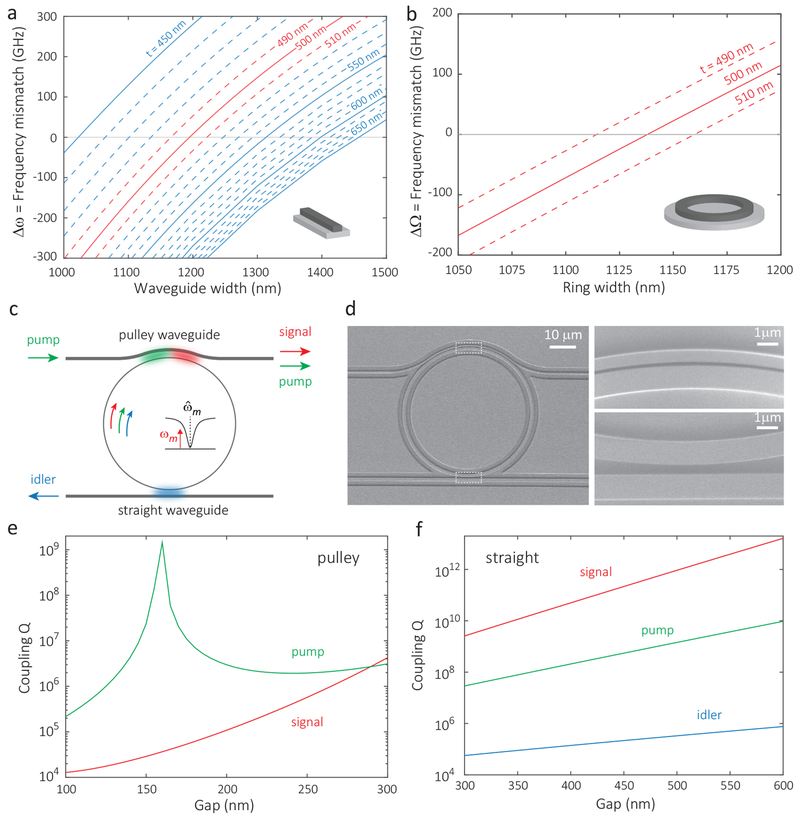
The core of the device is a high-Q Si3N4 microring with three key parameters - Si3N4 film thickness, ring width, and ring radius. The dispersion of the optical modes in the device is fully determined by these three parameters, given ellipsometric measurements of the wavelength-dependent refractive index of the Si3N4 and SiO2 layers. We first carry out a waveguide simulation with the first two parameters to estimate the frequency mismatch, as shown in Fig. 2(a). The frequency mismatch is calculated by the finite-element method as Δω= [(nsωs + niωi)/(2np)] − ωp, where ns, np, and ni are the effective indices at the frequencies ωs, ωp, and ωi (corresponding wavelengths of 668.4 nm, 934.0 nm, and 1550.0 nm, respectively, for signal, pump, and idler modes). For a device with a larger thickness, the ring width needs to be smaller for the geometric dispersion to compensate the material dispersion. At a Si3N4 thickness of 500 nm, the targeted ring width is about 1200 nm. We then run full simulations for the Si3N4 microring with a radius of 25 μm to find the optical modes around the targeted wavelengths, which have mode numbers of 443, 303, and 163, respectively. These mode numbers satisfy 2mp = ms + mi, and their corresponding resonances are close to the targeted frequencies (within one FSR). The frequency mismatches calculated from the ring simulations Δω = ωp − (ωs + ωi)/2 are plotted in Fig. 2(b), where the bending effect yields additional geometric dispersion that offsets the targeted geometry from that determined from waveguide simulations in Fig. 2(a). For a device thickness of 500 nm, the targeted ring width is around 1140 nm.
FIG. 2: Design and Simulation.
a, b, Simulated frequency mismatch (Δω = ωp − (ωs + ωi)/2) for phase-matched pump, signal, and idler modes (2mp = ms + mi), as a function of ring waveguide width (x-axis) and thickness t (different displayed curves). Calculations are based on (a) a model in which straight waveguide dispersion (no bending effect) is used, and (b) a full model in which the ring dispersion is used. The signal photon is at 668 nm, the idler photon is in the 1550 nm band, and the pump is in the 930 nm band. c, Waveguide-resonator coupling scheme, d, Scanning-electron-microscope images of a fabricated device with pulley waveguide on top, for injecting the 930 nm band pump and extracting the 660 nm band signal, and straight waveguide on bottom, for extracting the 1550 nm band idler, e, f Simulation of the coupling Qs of the pulley waveguide and straight waveguide, for the pump/signal and pump/signal/idler, respectively (the pulley waveguide does not support a mode at the idler wavelength).
Coupling Design
The wide spectral separation of the SFWM process in this work also poses a challenge for the resonator-waveguide coupling design. To couple visible, pump, and telecom modes efficiently, we employ two waveguides that separate the coupling tasks with the scheme shown in Fig. 2(c). A scanning-electron-microscope (SEM) image of the device is presented in Fig. 2(d). The top pulley waveguide is wrapped around the microring (Fig. 2(e)) to provide the extra interaction length needed to couple the pump and visible modes efficiently at the same time. This waveguide has a width of 560 nm, which supports single mode operation for the pump mode, and is cut-off for the telecom mode, a consequence of the asymmetric cladding (above a certain wavelength, not even a fundamental mode is guaranteed). Figure 2(g) shows the calculated coupling Q (using the coupled mode theory approach as in Refs. 22,25) of this pulley waveguide for the pump and signal modes, as a function of coupling gap and for a coupling length of 33 μm. For gaps between 200 nm to 250 nm, the pump mode is close to critical coupling and the signal mode is slightly over-coupled for intrinsic Qs around one million. The bottom straight waveguide (Fig. 2(f)) is used to out-couple the telecom mode and it has a width of 1120 nm. This width supports single mode operation at telecom wavelengths, and as shown in Fig. 2(h), the coupling gap for the straight waveguide can be tuned to couple the telecom mode only, while not coupling pump and signal modes (they are severely undercoupled), for optical modes with intrinsic Q around a million.
Mode Identification
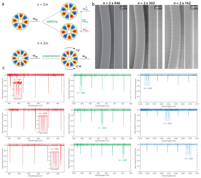
The dispersion design presented in the previous sections is targeted to specific mode numbers and cavity frequencies. Such unambiguous knowledge of optical mode numbers is absent in traditional transmission measurements of whispering gallery mode resonators. Here, we employ a method of mode splitting to identify the mode numbers26, by introducing a sinusoidal modulation of the form δr = αcos(nϕ) to the inside boundary of the microring (Fig. 3(a)–(b)). When the modulation index n does not line up with the azimuthal order m of the optical mode (bottom panel of Fig. 3(a), n ≠ 2m), the perturbation is not in phase with the optical mode, and thus any reflection induced by the perturbation does not coherently build up. Therefore, in this case, the optical mode (both clockwise and counterclockwise) remains unperturbed. In contrast, when the modulation index lines up with the azimuthal order of the optical mode so that n = 2m, the phase degeneracy is removed and the clockwise and counterclockwise optical modes are renormalized into two modes (top panel of Fig. 3(a)). One mode is located near the outside of the modulation and has a larger frequency, while the other mode is located near the inside of the modulation and has a smaller frequency. This splitting in frequency is proportional to the modulation amplitude. At a modulation amplitude of 50 nm (Fig. 3(b)), the frequency splitting is much larger than the cavity linewidth and is therefore visible in the transmission spectra. Thus, by changing the modulation period, the optical mode numbers can be identified, as shown in Fig. 3(c) for modes in the signal, pump, and idler bands. The Q of modes in the ring-width-modulated resonators is still reasonably high (Q > 105), so that one could envision using this approach to split modes that are some small number of FSRs away from the targeted ones, enabling their mode identification. However, as we would like to use as high-Q resonances as possible for pair generation, we instead use the mode splitting approach on test devices that are fabricated on the same chip as the devices in which we generate photon pairs. The good reproducibility of device fabrication across a chip ensures that these test mode splitting devices have spectra that are well-matched to the photon pair generation devices.
FIG. 3: Mode Number Identification.
a, Principle of azimuthal mode number identification by mode splitting. The mode splitting is created by periodic modulation of the inside boundary of the microring, of the form δr = αcos(nϕ). When the modulation index n is in phase with the azimuthal order of the mode m (top), so that n = 2m, frequency splitting occurs. When n ≠ 2m, the optical modes are unperturbed (bottom). b, Zoomed-in SEM images of the mode splitting devices in the signal (left), pump (center), and telecom (right) bands, in which an inner modulation amplitude α = 50 nm is applied. The approximate modulation period in the three cases is 170 nm, 250 nm, and 460 nm, respectively. c, Measured transmission spectra from Si3N4 microrings fabricated with the inner boundary modulation, in the signal (visible), pump (930 nm), and telecom bands, where the modulation has been varied across the spectra to target the labeled mode numbers.
Phase/Frequency-Matching
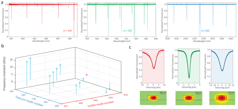
Through the mode number identification process, it is straightforward to find the targeted modes and calculate their frequency mismatch. Figure 4(a) shows the normalized cavity transmission for a fabricated device in the signal, pump, and idler bands, respectively. The frequency mismatch of various configurations that satisfy mode number matching are shown in Fig. 4(b). The targeted optical modes, shaded in Fig. 4(a), have azimuthal mode numbers ms = 443, mp = 303, and mi = 163. The wavelengths of the modes, measured by a wavemeter with an accuracy of 0.1 pm, are 668.3789 nm, 933.6211 nm, and 1547.8960 nm. The loaded Qs of the three modes, displayed in Fig. 4(c), are (1.52 ± 0.02) × 105, (1.04 ± 0.02) × 106, and (1.93 ± 0.04) × 105, corresponding to loaded cavity linewidths of (2.95 ± 0.04) GHz, (0.31 ± 0.01) GHz, and (1.00 ± 0.02) GHz, respectively. The uncertainties indicate 95 % confidence ranges of the nonlinear fitting. The frequency mismatch of the targeted mode (Δω = ωp − (ωs + ωi)/2) is only (0.16 ± 0.04) GHz (colored by red in Fig. 4(b), and the uncertainty arises from the wavemeter resolution of 1 pm), which is smaller than the cavity linewidths. Thus both phase- and frequency-matching are satisfied and the targeted SFWM process is permitted.
FIG. 4: Phase/Frequency-Matching.
a, Transmission spectrum of the microring resonator in the signal (visible), pump (930 nm), and idler (telecom) bands. The targeted modes for photon pair generation are highlighted, with their azimuthal mode numbers labeled. b, Frequency mismatch Δω = ωp − (ωs + ωi)/2, determined from wavemeter measurements in which the pump mode is fixed (mp =303) and the signal and idler modes vary in a way to maintain mode number matching (2mp = ms + mi). c, Zoomed-in transmission spectra of the targeted optical modes, with Lorentzian fits in black. Insets show cross-sectional views of the simulated dominant electrical field component (in the radial direction) of each mode.
Photon Pair Generation
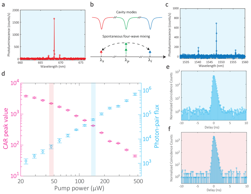
Given the match of mode numbers and cavity frequencies as shown in Fig. 4, we now consider the generation of photon pairs. Continuous-wave light from an external cavity diode laser is used to pump the cavity mode at 933.6 nm, and the spectrum of SFWM is measured using two grating spectrometers, one to cover the visible wavelength band and one to cover the telecommunications wavelength band (see Supplementary Material and Methods). Emission from cavity modes at 1547.9 nm and 668.4 nm is observed in the spectrometers (spectral resolution is ≈100 pm), along with two adjacent sets of pairs (Fig. 5(a)–(c)). These auxiliary pairs are both mode number matched, but are weaker in amplitude due to the larger frequency mismatch. For example, the photon pair at 667.0 nm (ms = 444) and 1555.2 nm (mi = 162) has a frequency mismatch of 3.86 GHz, as shown in Fig. 4(d), which is about 10 × larger than that of the brightest pair.
FIG. 5: Visible-Telecom Photon Pair Generation.
a, c, Spectrum of spontaneous four-wave-mixing in the visible and telecom bands, respectively, based on the photon pair generation scheme shown in b. d, Pump-power-dependence of the visible-telecom photon pair source coincidence-to-accidental ratio (CAR) and on-chip photon pair flux. Error bars are one standard deviation uncertainties resulting from fluctuations in the detected count rates, e, f, Coincidence counting trace for the two highlighted points in d (background color matches the highlighting color). The time bin is 128 ps. The mean background level (i.e., accidental counting) is normalized to 1 in these plots.
We next use coincidence counting measurements to characterize the quality of the generated photon pairs. The large spectral separation between pump, signal, and idler makes this task straightforward, as the photons can be easily separated by edgepass filters or broadband demultiplexers. Moreover, the spectra in the signal and idler bands exhibit limited influence from amplified spontaneous emission (ASE) and Raman noise, which are adjacent to the pump band and do not extend far enough spectrally to strongly influence the pairs. As a result, no broadband noise is observed in either the visible or telecom bands.
For coincidence counting, two filters are used to select the targeted spectral channels before they are detected on single photon detectors (see Supplementary Material for details). Figure 5(d) presents the pump-power-dependence of the photon-pair flux at the waveguide output and the coincidence-to-accidental ratio (CAR). When the pump power is below 46 μW, the CAR value is above (2.20 ± 0.05) × 103 and the photon pair flux is below (4.8 ± 0.9) × 103, where the uncertainties are one standard deviation values based on the fluctuation in detected count rates. The highest CAR measured is (3.8 ± 0.2) × 103 at a flux of (1.2 ± 0.3) × 103 counts per second. This CAR value is two orders of magnitude higher than those of previously demonstrated visible-telecom photon pair sources based on photonic crystal fiber9 and millimeter-scale crystalline disks11. When the pump power is above 146 μW, the CAR value is below (422 ± 5) and the photon pair flux is above (6.2 ± 0.5) × 104 counts per second. At pump powers above 290 μW, the photon pair flux shows a weaker increase than expected based on the slope of the lower power data, and is due to optical parametric oscillation in the pump band (see Supplementary Material). This effectively serves as a competing process that results in a reduced conversion efficiency from the pump to visible-telecom photon pairs. Finally, Fig. 5(e)–(f) shows normalized coincidence spectra that correspond to two of the aforementioned cases, with CAR values of (422 ± 5) and (2.20 ± 0.05) × 103, respectively. The asymmetry in the coincidence peak is a result of the difference in photon lifetimes in the telecom and visible bands (approximately a factor of 3).
Wavelength-Tunable Photon Pairs
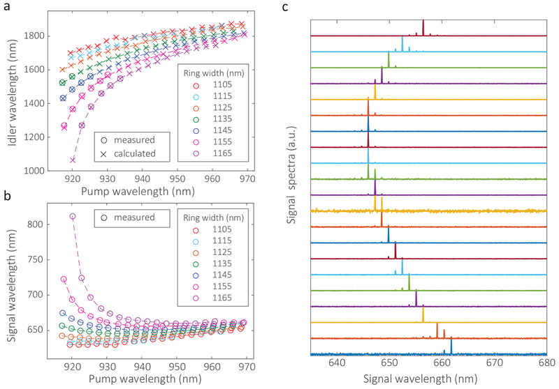
We have thus far focused on the generation of photon pairs according to a design that connects the 660 nm band with the 1550 nm band. However, the approach we have developed for engineering these sources is general, and one can easily envision extending it to connect other sets of wavelengths of interest. As an example, we demonstrate tuning of the photon pair wavelengths through two experimental parameters, the pump wavelength (adjustable on a given device) and ring width (adjustable between devices on the same chip). Figure 6 shows the results, in which the pump wavelength is varied between 920 nin and 970 nm, and the ring width between 1105 nm and 1165 nm. As shown in Fig. 6(b)–(c), the visible photons shift from 630 nm to 810 nm, while the accompanying idler photon wavelength changes from 1800 nm to 1200 nm (Fig. 6(a)). These sources span a significant fraction of the physical systems shown in Fig. 1(c), including systems like the nitrogen vacancy center in diamond, the silicon vacancy center diamond, and the D1 and D2 transitions in Rb.
FIG. 6: Wavelength Tuning of the Photon Pair Sources.
Dependence of a idler wavelength and b signal wavelength, generated by pumping microrings with varying ring widths on cavity modes across the 920 nm to 970 nm pump band. Measured data points are shown by ◯ symbols. As the telecom band spectrometer is limited to the 1200 nm to 1600 nm range, idler wavelengths that lie above this wavelength range are calculated (shown by × symbols) based on the measured pump and signal wavelengths. c, Spectrum of SFWM in the visible wavelength band for a fixed ring width and a series of different pump wavelengths.
Discussion
We have demonstrated, for the first time, the ability to engineer on-chip nanophotonic resonators to create photon pair sources with a wide spectral separation between signal and idler, so that one photon is in the visible and the other in the telecom. We use the Si3N4/SiO2/Si platform to enable this work, due to its large Kerr nonlinearity, broadband optical transparency, and strong ability to engineer dispersion through geometric (waveguiding and bending) effects. After performing electromagnetic simulations to identify sets of microring resonator modes that can satisfy both phase-matching (mode number matching) and frequency matching, we utilize a mode identification technique that allows us to experimentally determine absolute azimuthal mode numbers in fabricated devices, thereby paving the way for the experimental demonstration of photon pair generation. Our photon pair sources generate bright and pure visible-telecom photon pairs with unprecedented CAR values at sub-mW pump power. By adjusting the pumping wavelength and device geometry, we show flexible tuning of the source wavelengths, with the visible photon of the pair moving from 630 nm to 810 nm. Through further development, we anticipate that these sources can be used in efforts to link distant quantum systems via entanglement swapping7.
Methods
Device Fabrication
The device layout was done with the Nanolithography Toolbox, a free software package developed by the NIST Center for Nanoscale Science and Technology27. The Si3N4 layer is deposited by low-pressure chemical vapor deposition of a 500 nm thick Si3N4 layer on top of a 3 μm thick SiO2 layer on a 100 mm Si wafer. The wavelength-dependent refractive index and the thickness of the layers are measured using a spectroscopic ellipsometer, with the data fit to an extended Sellmeier model. The device pattern is created in ZEP520A positive-tone resist by electron-beam lithography28. The pattern is then transferred to Si3N4 by reactive ion etching using a CF4/CHF3 chemistry. The device is chemically cleaned to remove deposited polymer and remnant resist, and then annealed at 1100 °C in an N2 environment for 4 hours. An oxide lift-off process is performed so that the devices are with air-cladding on top but the input/output waveguides are with oxide-cladding on top. The edge of the chip is then polished for lensed-fiber coupling. After the polishing, the chip is annealed again at 1100 °C in an N2 environment for 4 hours.
CAR
The CAR values in Figure 5(d) are calculated by CAR=(C-A)/A, where C and A are the overall and accidental coincidence counts extracted from the peak and background of the coincidence counting spectra (Fig. 5(e,f)), respectively. The one standard deviation uncertainty in CAR σCAR is given by , where σE and σA are the one standard deviation uncertainties in the measured overall coincidence counts and accidental coincidence counts, respectively. The above approximation is made possible as σC/C ⪢ σA/A. A is the mean value taken over a 4 μs time window in the coincidence counting trace. σA is determined from 20 sections of coincidence counting backgrounds, each of which spans 200 ns.
Supplementary Material
Acknowledgements
X.L., Q.L., G.M., and A.S. acknowledge support under the Cooperative Research Agreement between the University of Maryland and NIST-CNST, Award no. 70NANB10H193.
Footnotes
Competing financial interests The authors declare no competing financial interests.
References
- 1.Gisin Nicolas and Thew Rob, “Quantum communication,” Nature Photonics 1, 165–171 (2007). [Google Scholar]
- 2.Lvovsky AI, Sanders BC, and Tittel W, “Optical quantum memory,” Nature Photonics 3, 706–714 (2009). [Google Scholar]
- 3.Simon C, Afzelius M, Appel J, Boyer de la Giroday A, Dewhurst SJ, Gisin N, Hu CY, Jelezko F, Kroll S, Muller JH, Nunn J, Polzik ES, Rarity JG, De Riedmatten H, Rosenfeld W, Shields AJ, Skold N, Stevenson RM, Thew R, Walmsley IA, Weber MC, Weinfurter H, Wrachtrup J, and Young RJ, “Quantum memories: A review based on the European integrated project Qubit Applications (QAP),” The European Physical Journal D 58, 1–22 (2010). [Google Scholar]
- 4.Miya T, Terunuma Y, Hosaka T, and Miyashita T, “Ultimate low-loss single-mode fibre at 1.55 um,” Electronics Letters 15, 106–108 (1979). [Google Scholar]
- 5.Raymer MG and Srinivasan K, “Manipulating the color and shape of single photons,” Physics Today 65, 32–37 (2012). [Google Scholar]
- 6.Pan J-W, Bouwmeester D, Weinfurter H, and Zeilinger A, “Experimental entanglement swapping: entangling photons that never interacted,” Physical Review Letters 80, 3891–3894 (1998). [Google Scholar]
- 7.Halder M, Beveratos A, Gisin N, Scarani V, Simon C, and Zbinden H, “Entangling independent photons by time measurement,” Nature Physics 3, 692–695 (2007). [Google Scholar]
- 8.Hensen B, Bernien H, Dreau AE, Reiserer A, Kalb N, Blok MS, Ruitenberg J, Vermeulen RFL, Schouten RN, C Abellan, Amaya W, Pruneri V, Mitchell MW, Markham M, Twitchen DJ, Elkouss D, Wehner S, Taminiau TH, and Hanson R, “Loophole-free Bell inequality violation using electron spins separated by 1.3 kilometres,” Nature 526, 682–686 (2015). [DOI] [PubMed] [Google Scholar]
- 9.Clausen C, Bussieres F, Tiranov A, Herrmann H, Silberhorn C, Sohler W, Afzelius M, and Gisin N, “A source of polarization-entangled photon pairs interfacing quantum memories with telecom photons,” New Journal of Physics 16, 093 058 (2014). [Google Scholar]
- 10.Soller C, Brecht B, Mosley PJ, Zang LY, Podlipensky A, Joly NY, Russell PSJ, and Silberhorn C, “Bridging visible and telecom wavelengths with a single-mode broadband photon pair source,” Physical Review A 81, 031 801 (2010). [Google Scholar]
- 11.Schunk G, Vogl U, Strekalov DV, Frtsch M, Sedlmeir F, Schwefel HGL, Gobelt M, Christiansen S, Leuchs G, and Marquardt C, “Interfacing transitions of different alkali atoms and telecom bands using one narrowband photon pair source,” Optica 2, 773–778 (2015). [Google Scholar]
- 12.Caspani L, Xiong C, Eggleton BJ, Bajoni D, Liscidini M, Galli M, Morandotti R, and Moss DJ, “Integrated sources of photon quantum states based on nonlinear optics,” Light: Science & Applications 6, e17 100 (2017). [DOI] [PMC free article] [PubMed] [Google Scholar]
- 13.Jiang WC, Lu X, Zhang J, Painter O, and Lin Q, “Silicon-chip source of bright photon pairs,” Optics Express 23, 20 884–20 904 (2015). [DOI] [PubMed] [Google Scholar]
- 14.Lu X, Jiang WC, Zhang J, and Lin Q, “Biphoton statistics of quantum light generated on a silicon chip,” ACS Photonics 3, 1626–1636 (2016). [Google Scholar]
- 15.Grassani D, Azzini S, Liscidini M, Galli M, Strain MJ, Sorel M, Sipe JE, and Bajoni D, “Micrometer-scale integrated silicon source of time-energy entangled photons,” Optica 2, 88–94 (2015). [Google Scholar]
- 16.Savanier M, Kumar R, and Mookherjea S, “Photon pair generation from compact silicon microring resonators using microwatt-level pump powers,” Optics Express 24, 3313–3328 (2016). [DOI] [PubMed] [Google Scholar]
- 17.Ramelow S, Farsi A, Clemmen S, Orquiza D, Luke K, Lipson M, and Gaeta AL, “Silicon-nitride platform for narrowband entangled photon generation,” arXiv: 1508.04358 (2015). [Google Scholar]
- 18.Jaramillo-Villegas JA, Imany P, Odele OD, Leaird DE, Ou Z-Y, Qi M, and Weiner AM, “Persistent energytime entanglement covering multiple resonances of an on-chip biphoton frequency comb,” Optica 4, 655–658 (2017). [Google Scholar]
- 19.Okawachi Y, Saha K, Levy JS, Wen YH, Lipson M, and Gaeta AL, “Octave-spanning frequency comb generation in a silicon nitride chip,” Optics Letters 36, 3398–3400 (2011). [DOI] [PubMed] [Google Scholar]
- 20.Li Q, Briles TC, Westly DA, Drake TE, Stone JR, Ilic BR, Diddams SA, Papp SB, and Srinivasan K, “Stably accessing octave-spanning microresonator frequency combs in the soliton regime,” Optica 4, 193–203 (2017). [DOI] [PMC free article] [PubMed] [Google Scholar]
- 21.Karpov M, Pfeiffer MHP, Liu J, Lukashchuk A, and Kippenberg TJ, “Photonic chip-based soliton frequency combs covering the biological imaging window,” Nature Communications 9 (2018). [DOI] [PMC free article] [PubMed] [Google Scholar]
- 22.Li Q, Davanco M, and Srinivasan K, “Efficient and low-noise single-photon-level frequency conversion interfaces using silicon nanophotonics,” Nature Photonics 10, 406–414 (2016). [Google Scholar]
- 23.Boyd RW, Nonlinear Optics (Elsevier, 2003). [Google Scholar]
- 24.Agrawal GP, Nonlinear Fiber Optics (Academic Press, 2007). [Google Scholar]
- 25.Shah Hosseini E, Yegnanarayanan S, Atabaki AH, Soltani M, and Adibi A, “Systematic design and fabrication of high-Q single-mode pulley-coupled planar silicon nitride microdisk resonators at visible wavelengths,” Optics Express 18, 2127–2136 (2010). [DOI] [PubMed] [Google Scholar]
- 26.Lu X, Rogers S, Jiang WC, and Lin Q, “Selective engineering of cavity resonance for frequency matching in optical parametric processes,” Applied Physics Letters 105, 151 104 (2014). [Google Scholar]
- 27.Coimbatore Balram K, Westly DA, Davanco MI, Grutter KE, Li Q, Michels T, Ray CH, Kasica RJ, Wallin CB, Gilbert IJ, Bryce BA, Simelgor G, Topolancik J, Lobontiu N, Liu Y, Neuzil P, Svatos V, Dill KA, Bertrand NA, Metzler M, Lopez G, Czaplewski D, Ocola L, Srinivasan KA, Stavis SM, Aksyuk VA, Liddle JAA, Krylov S, and Ilic RR, “The nanolithography toolbox,” Journal of Research of the National Institute of Standards and Technology 121, 464–475 (2016). [DOI] [PMC free article] [PubMed] [Google Scholar]
- 28.The identification of any commercial product or trade name is used to foster understanding. Such identification does not imply recommendation or endorsement or by the National Institute of Standards and Technology, nor does it imply that the materials or equipment identified are necessarily the best available for the purpose.
Associated Data
This section collects any data citations, data availability statements, or supplementary materials included in this article.


