Abstract
Transition metal dichalcogenide two-dimensional materials have attracted significant attention due to their unique optical, mechanical, and electronic properties. For example, molybdenum disulfide (MoS2) exhibits a tunable band gap that strongly depends on the numbers of layers, which makes it an attractive material for optoelectronic applications. In addition, recent reports have shown that laser thinning can be used to engineer an MoS2 monolayer with specific shapes and dimensions. Here, we study laser-thinned MoS2 in both ambient and vacuum conditions via confocal μ-Raman spectroscopy, imaging X-ray photoelectron spectroscopy (i-XPS), and atomic force microscopy (AFM). For low laser powers in ambient environments, there is insufficient energy to oxidize MoS2, which leads to etching and redeposition of amorphous MoS2 on the nanosheet as confirmed by AFM. At high powers in ambient, the laser energy and oxygen environment enable both MoS2 nanoparticle formation and nanosheet oxidation as revealed in AFM and i-XPS. At comparable laser power densities in vacuum, MoS2 oxidation is suppressed and the particle density is reduced as compared to ambient. The extent of nanoparticle formation and nanosheet oxidation in each of these regimes is found to be dependent on the number of layers and laser treatment time. Our results can shed some light on the underlying mechanism of which atomically thin MoS2 nanosheets exhibit under high incident laser power for future optoelectronic applications.
Keywords: molybdenum disulfide, X-ray photoelectron spectroscopy, confocal Raman spectroscopy, atomic force microscopy, nanoparticles, laser irradiation
Graphical Abstract
INTRODUCTION
Two-dimensional materials such as graphene and transition metal dichalcogenides (TMDCs) have been extensively studied in the past few years due to their exceptional mechanical, electrical, and optical properties.1–3 In some applications, TMDCs are preferred over graphene, given that graphene lacks a band gap. Moreover, TMDCs such as molybdenum disulfide (MoS2) exhibit a tunable band gap, which depends on the number of layers.4 Due to weak van der Waals forces between the layers, it is possible to mechanically exfoliate layered TMDCs from their bulk form.4,5 The resulting atomically thin MoS2 nanosheets have demonstrated extraordinary electronic, photonic, and thermoelectric properties, which makes layered MoS2 a strong candidate for various electronic and optoelectronic applications.6–9
As a result, several groups have been developing different methods by which to engineer and control the number of layers of MoS2.10–14 Most notably, Liu et al. demonstrated layer-by-layer thinning using argon plasma.15 Their data show a reliable thinning of layered MoS2 down to a monolayer. Gomez et al. showed laser thinning of the MoS2 layers that had been mechanically exfoliated from a macroscopic MoS2 crystal. The authors confirmed the formation of monolayers with a desired shape, an attractive method to engineer MoS2 nanosheets.16 However, their Raman results suggest that no oxidized MoS2 peaks were observed, which led them to conclude that no oxide layers were formed after laser thinning.
Most recently, Lee et al. measured the photoluminescence (PL) modulation of laser-treated monolayer MoS2.17 In that study, the authors established the three stages of photooxidation associated with laser irradiation periods in ambient conditions. The measurements showed a large PL modulation in the first step of oxidation, followed by a PL decrease and quenching. The trends were associated with structural damage and oxygen adsorption on the MoS2 surface. However, the mechanism and implications behind the physical transformations of MoS2 nanosheets by laser treatment were still unclear. Moreover, recent work on MoS2 nanosheets have shown anomalous particles forming on the surface of the layered material after laser irradiation.18 Their characterization results showed that the particle density depends on the laser irradiation power, the laser irradiation time, and the number of layers. Still, the origin of these anomalous nanoparticles is unclear.
Here, we study laser-thinned MoS2 in both ambient and vacuum conditions via confocal μ-Raman spectroscopy, imaging X-ray photoelectron spectroscopy (i-XPS), and atomic force microscopy (AFM). For low laser powers in ambient conditions, it is shown that there is insufficient energy to oxidize the MoS2 surface, but sufficient energy to etch and redeposit anomalous MoS2 nanoparticles. In contrast, at high powers in ambient conditions, the laser energy and oxygen environment facilitate MoS2 nanoparticle formation and nanosheet oxidation. Finally, at comparable power densities in vacuum, MoS2 oxidation is suppressed, and the nanoparticle density is reduced relative to ambient experiments. Thus, we deduce that the formation of the anomalous MoS2 nanoparticles is not limited to a specific environment, whereas MoS2 oxidation is only possible in an oxygen environment (e.g., ambient conditions). Furthermore, the anomalous Raman trends are explained in terms of the observed physical changes to the MoS2 surface, and attributed to changes in electron–phonon coupling for monolayers and electron–photon coupling for multilayers. Overall, the unique combination of techniques sheds light on the physicochemical reasons for the observed properties of MoS2 nanosheets after laser irradiation, which has significant implications for future TMDC-based applications.
RESULTS
Raman Characteristics of Laser-Thinned MoS2 Nano-sheets.
Figure 1a shows the setup for the laser thinning process. This laser thinning technique enabled us to engineer monolayer MoS2 with the desired size and shape. The optical images of the targeted MoS2 nanosheet before and after laser thinning are shown in Figure 1b,c, respectively. The initial thickness of the flake is estimated to be >5L based on the difference between the A1g and E2g Raman peak positions (Figures 1d and S1b–e).19 After laser thinning, the nanosheet reveals characteristics of a bilayer (2L), as evident by the shifts in the A1g and E2g peaks in Figure S1b. All the Raman measurements were collected after laser thinning. In Figure S1a, we show the Raman measurements at different incident energy densities (energy per unit area) using a 532 nm laser on a 130 nm thick nanosheet. In this figure, the highlighted parts show the number of layers based on the difference in the Raman peaks for A1g and E2g , as previously reported.19 The estimated etching rate is shown in the inset of the figure and varies with the number of layers etched. This variability in the etching rate with increased number of layers is likely due to strong interlayer coupling between MoS2 layers.
Figure 1.
Exfoliated MoS2 nanosheets. (a) Schematic illustration of the Raman setup used to treat and measure MoS2 nanosheets. Optical images taken (b) before and (c) after laser thinning of the MoS2 nanosheet. Raman intensity maps of MoS2 and MoO3 vibrational peaks (d) before and (e) after laser thinning of the MoS2 nanosheet.
To evaluate the formation of oxide on the MoS2 surface, we also spatially mapped the Raman intensities at 289 and 820 cm−1, both of which have been associated with MoO3.20 At these two peak positions, there is no observable Raman signal in the maps (Figure 1e) or spectra (Figure S1), which could imply that (1) an oxide layer did not form or (2) the oxide layer is not in the form of MoO3.
i-XPS Measurements of Native and Laser-Treated MoS2 Nanosheets Under Different Environmental Conditions.
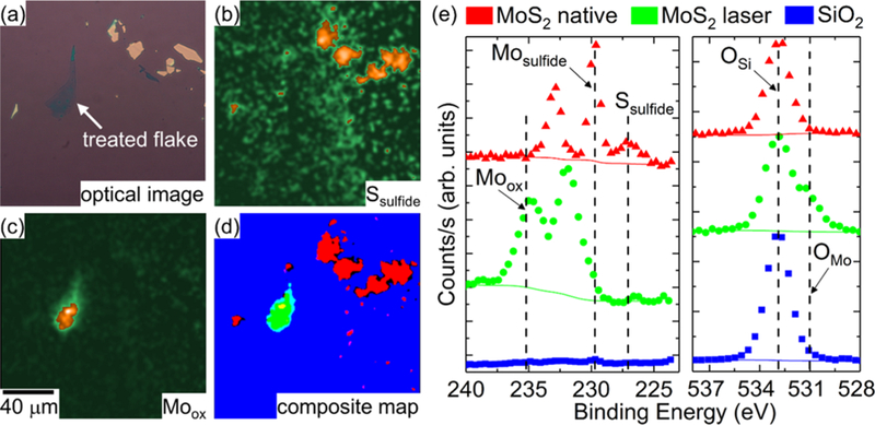
i-XPS was performed on native and laser-treated MoS2 flakes. Figure 2 shows the results from the processed i-XPS measurements on native and laser-treated MoS2 nano-sheets in ambient conditions, as shown in the optical images in Figure 2a. Ambient, in this study, is synonymous with an air environment. Analysis of the images around the S 2s region at ≈227 eV reveals that the native flakes retained sulfur content (Figure 2b), suggesting that their surface composition is still consistent with MoS2. Additionally, images associated with the Mo 3d5 peak maximum near 229.8 eV, attributed to MoS2, further corroborates this result (as shown in Figure S2a). In contrast, there is no significantly increased signal intensity observed in the region treated with 8.3 mW (high) laser power attributed to sulfide or MoS2. However, there is evidence of an Mo 3d signal at around 235 eV, attributed to the 3d3 peak associated with oxidized MoS2 (MoxOy), which is only present at the treated flake (Figure 2c). To extract spectra from the raw unprocessed images, masks were created from the Ssulfide, Moox, and SiO2 images to identify regions of interest (ROI) with minimal overlap attributed to the native and laser-treated MoS2 flakes, as well as the substrate (Figure 2d).
Figure 2.
i-XPS measurements on native and laser-treated MoS2 nanosheets treated in ambient conditions. (a) Optical image of the area containing native and laser-treated nanosheets. (b) Processed image attributed to Ssulfide 2s signal. (c) Processed image attributed to Moox 3d3 signal. (d) Composite map of masks associated with processed images of Moox (green), Ssulfide (red), and SiO2 (blue) signals. Yellow, teal, and pink reflect an overlap in masks, whereas black reflects an absence in masks. (e) i-XPS spectra from the raw images based on pixels from the ROIs defined in the composite map. The Mo 3d and S 2s regions (left) and the O 1s region (right).
Spectra for Mo 3d, S 2s, and O 1s regions associated with pixels from each mask are provided in Figure 2e, whereas the Si 2p region, used principally for energy correction, is provided in the Supporting Information (SI) (Figure S3). Indeed, Mo 3d5 and S 2s spectra (left) for the native, untreated flakes exhibit peak maxima at 229.8 eV and 227.0 eV, respectively, consistent with literature values for the photoelectric transitions for MoS2, in a ratio of 1.9:1 after correcting for the sensitivity factors that relate to the different cross sections for photoemission.21 In contrast, sulfur is undetectable in the laser-treated MoS flakes, with only slight increases in signal intensity attributed to the satellite peaks for the shifted Moox 3d3 peak, suggesting that the sulfide characteristics are completely removed. Indeed, the molybdenum spectra shift in peak maximum by roughly 2 eV to 231.8 eV for the Moox 3d5 feature. Notably, the spectral features broaden in full width at half-maximum (FWHM), suggestive of a distribution of oxide (IV–VI) species within the spectral envelope. However, because MoO2 is found at the binding energies proximate to MoS2 and MoO3 is typically found at positions 0.5–1.0 eV higher in binding energy, we suspect there is a significant contribution from an intermediary oxide component, such as Mo2O5, which has been demonstrated to be present near the observed fitted peak position.22–24
Consistent with the observed transformations in the Mo and S spectra, the O 1s window also transforms from one Gaussian-like feature to two features when comparing native and treated spectra, respectively. This reflects the difference between oxygen attributed to the SiO2 (OSi) and the oxidized molybdenum (OMo) at peak positions of 532.9 eV and 531.0 eV, respectively. The OMo/Moox value is approximately 2.1:1, suggesting either the existence of oxygen vacancies or that the fit of the spectra is imperfect. Table S1 provides additional detail on the relative atomic percentages associated with the fitted spectra extracted from ROIs in the composite map for native and laser-treated MoS2 flakes (fitted spectra available in Figure S4). Although these values are only estimates and accordingly lack uncertainty due to factors explained in the SI and Methods section, we thought it important to demonstrate the degree of agreement between experimentally derived values and theoretical values. It is also important to note two points regarding the formation of a Moox layer: (1) the result regarding MoS2 oxidation has been replicated in another measurement, demonstrating the repeatability of the finding (see Figure S5) and (2) the dominant signs of Mo oxidation are not observed when the laser thinning is performed at lower powers such as 0.93 mW (data not shown).
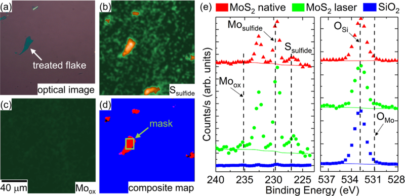
Figure 3 shows the results from i-XPS measurements on native MoS2 flakes and MoS2 flakes laser-treated with 7.2 mW (high laser power) in vacuum conditions. The imaged region contains both native and laser-treated MoS2 flakes, with the laser-treated flake near the middle of the analysis area (Figure 3a). As shown in Figure 3b, the images reveal a significant sulfur contribution remained, as evident from the well-defined Ssulfide region (see Figure S2b,d for MoS2 and Si 2p for the processed images). The Moox image was devoid of any large localized contributions at the 235.0 eV peak position (Figure 3c). Together, these observations suggest that the surface was substantially less photochemically transformed than in the previous ambient experiments. Because the composite map lacks a well-defined ROI for Moox, a manually selected ROI (green rectangle) was made in addition to the SiO2 mask and the Ssulfide mask (Figure 3d).
Figure 3.
i-XPS measurements on native and laser-treated MoS2 nanosheets treated in vacuum. (a) Optical image of the area containing native and laser-treated nanosheets. (b) Processed image attributed to Ssulfide 2s signal. (c) Processed image attributed to Moox 3d3 signal. (d) Composite map of masks associated with processed images of Moox (green), Ssulfide (red), and SiO2 (blue) signals. (e) i-XPS spectra from the raw images based on pixels from the ROIs defined in the composite map. The Mo 3d and S 2s regions (left) and the O 1s region (right).
Analysis of the spectra reveal only minimal differences between the spectra from the sulfide mask and the spectra from the manually selected laser-treated area (Figures 3e and S3b for Si 2p). Indeed, this suggests that in the presence of vacuum, the laser-treated sections remain MoS2. Both the native and laser-treated MoS2 spectra reveal a S/Mosulfide relative sensitivity factor-adjusted intensity of roughly 1.8 under vacuum conditions (Table S1). Based on the fitting, a small amount of MoxOy may be present in the treated section; however, it is impossible to differentiate this from the noise with any reasonable certainty.
AFM and Raman Measurements of Laser-Treated MoS2 Nanosheets.
Figure S6 shows the morphology of a laser-thinned MoS2 nanosheet. The optical image of the targeted nanosheet is highlighted in the image of Figure S6a. The power and time used for laser thinning is analogous to the reported values above in an ambient environment. The AFM results in Figure S6 show a clear transition from multilayer MoS2 to monolayer MoS2, confirming our Raman results obtained before and after thinning. The AFM results can be interpreted by examining Figure S6b–d, which cover three major regions: native, at the edge of the native and thinned regions, and postlaser thinning region, respectively. These regions are highlighted in the AFM image of Figure S6a. In Figure S6c, a clear transition from multilayer to monolayer is observed. Moreover, it is found that the roughness of the nanosheet significantly increased after thinning, as shown in Figure S6d.
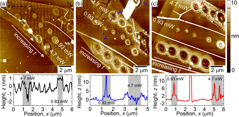
Figure 4 illustrates the morphology of laser-treated monolayers, three layers (3L), and five layers (5L) of MoS2 nanosheets. In this figure, laser treatments are targeted at specific spots on the surface of the MoS2 nanosheet using a 532 nm laser with varying optical powers and treatment times, as labeled in Figure 4a–c. For all layers, the AFM results show an instant thinning for laser powers of 4.7 and 8.3 mW regardless of the treatment time. However, for 0.93 mW, we see the formation of anomalous particles around the treatment sites. In fact, we observe nanoparticles forming around all the treatment points. These nanoparticles have been reported previously and their volume has been shown to depend on the number of layers and the treatment conditions.18 In Figure S14, we show the SEM images of some laser-treated MoS2 sites. Our results show consistency in the nanoparticle formation with laser power and treatment time, supporting the previous report.
Figure 4.
AFM images and cross sections of (a) one layer (1L), (b) 3L, and (c) 5L MoS2 nanosheets laser-treated in ambient conditions.
The Raman characteristics measured after treating MoS2 nanosheets are shown in Figure 5a–c for 1L, 3L, and 5L, respectively. Raman measurements are collected after laser treatments. In these figures, we plot the Raman characteristics versus the treatment time for 0.93 mW laser power. We notice that for 3L and 5L, the intensity of the A1g and E2g peaks drop equally, whereas the FWHM of each peak increases slightly. The Raman shift for both peaks does not show any shift. However, the monolayers exhibit a different behavior, as shown in Figure 5a. The Raman shift for the A1g peak shows a slight upshift, which is also observed on different samples as in Figure S7, whereas the Raman shift for the E2g peak does not show noticeable shift within the measurements sensitivity. Moreover, the intensity of the A1g peak exhibits a different behavior than the E2g peak. In fact, the E2g peak shows a significant decrease in intensity as compared to the A1g peak. Other 1L samples show similar effects. The linewidth (FWHM) for the A1g peak decreases with increasing treatment time, whereas the E2g linewidth is constant. This anomalous behavior has been observed previously in laser-irradiated MoS2 and was attributed to p-doping of the monolayer.17 However, this explanation does not take into consideration the effect of the photoinduced nanoparticles on the measured Raman characteristics. This point will be addressed in the Discussion section.
Figure 5.
Raman intensity, linewidth (FWHM), and shift of (a) 1L, (b) 3L, and (c) 5L MoS2 nanosheets laser-treated in ambient conditions.
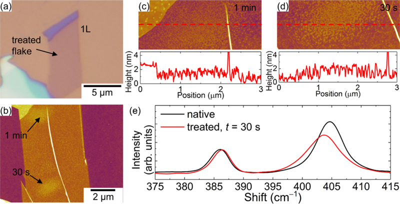
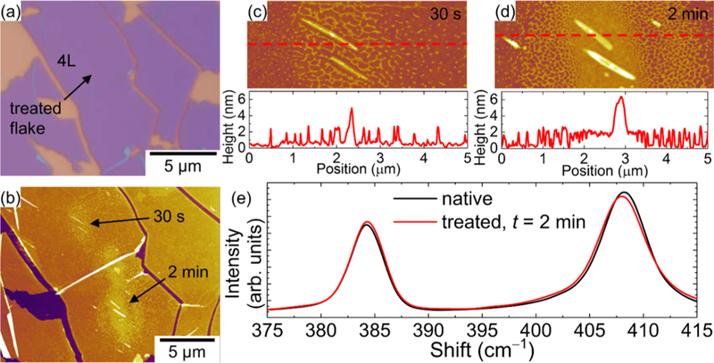
To better understand the anomalous nanoparticles, the surface morphology and the Raman characteristics of laser-treated MoS2 were measured at similar energy densities in vacuum. Figures 6 and 7 show the laser-treated monolayer and four layer (4L) MoS2 nanosheets in vacuum, respectively. Remarkably, we are able to produce these nanoparticles with similar power density and at different treatment times. The density of the nanoparticles increases with treatment time. Figures 6e and 7e show the Raman spectra before and after treatments for 1L and 4L MoS2, respectively. The Raman shift of the A1g peak for 1L postlaser treatment is downshifted and broadened, indicative of heating. However, for the 4L nanosheet, despite the existence of photoinduced nanoparticles on the surface of the MoS2, the Raman characteristics lack any noticeable change with treatment time, which can be attributed to a strong interlayer coupling.
Figure 6.
AFM images and Raman measurements on 1L MoS2 nanosheets laser-treated in vacuum. (a) Optical image and (b) AFM image of laser-treated MoS2 nanosheet. Higher-magnification AFM images of each treatment locations for (c) 1 min and (d) 30 s laser treatments. (e) Raman spectra before and after the 30 s laser treatment.
Figure 7.
AFM images and Raman measurements on 4L MoS2 nanosheets laser-treated in vacuum. (a) Optical image and (b) AFM image of laser-treated MoS2 nanosheet. Higher-magnification AFM images of each treatment locations for (c) 30 s and (d) 2 min laser treatments. (e) Raman spectra before and after the 2 min laser treatment.
In Figures S7–S9, the Raman characteristics and topography after laser-treating additional 1L MoS2 in different environments are shown. The Raman characteristics of laser-treated MoS2 in ambient and vacuum are shown in Figures S7 and S8, respectively. We observe similar behavior as the results demonstrated in Figures 6 and 7. The Raman shift for the A1g mode downshifts and broadens in the vacuum environment with increasing treatment times, whereas the mode upshifts and becomes narrower (reduced linewidth) after laser treatments in ambient. The opposing behavior in ambient and vacuum can be attributed to the formation of photoinduced nanoparticles as discussed below. Based on the AFM before and after treatments in Figure S9, we deduce that the formation of the nanoparticles is not restricted to a specific environment. Nonetheless, we see a decrease in particle density for laser-treated MoS2 in vacuum compared to air. The reason behind this change in the particle density is still unclear. However, we suspect that the significant reduction in oxygen in the chamber can affect the physioadsorption mechanism, leading to reduced particle density.
DISCUSSION
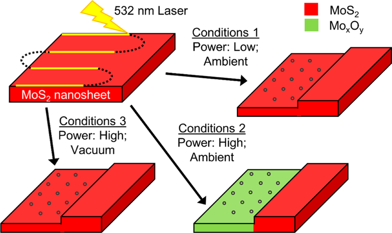
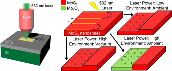
Figure 8 illustrates a proposed mechanism when a laser with certain power is incident on an MoS2 nanosheet. For low laser power and in an ambient environment, there is not enough energy to oxidize MoS2, which leads to etching and possibly redeposition of amorphous MoS2 on the surface of the nanosheet. In contrast, at high powers in ambient conditions, the laser energy and oxygen environment enable both MoS2 nanoparticle formation and nanosheet oxidation. However, when this high laser power is incident on an MoS2 nanosheet in vacuum, no oxidation occurs due to the lack of oxygen. Hence, only etching redeposition of amorphous MoS2 nanoparticles on the surface occurs. Accordingly, based on this mechanism, two major factors are necessary for MoS2 oxidation: high laser power and oxygen; however, relatively low laser power (0.93 mW) for at least 60 s, regardless of the environment, can induce nanoparticles on the surface of the nanosheet.
Figure 8.
Laser-induced thinning conditions mostly result in nanoparticle formation (blue circles) on a MoS2 surface; however, different conditions impact surface chemistry. (1) Low-power laser and the presence of atmospheric oxygen retains the MoS2 chemical structure. (2) High-power laser and the presence of atmospheric oxygen results in molybdenum oxidation. (3) High-power laser in the presence of vacuum also retains MoS2 chemical structure.
The anomalous Raman intensity behavior for A1g and E2g of laser-treated monolayers can be explained by considering the various terms that affect the Raman intensity characteristics. The Raman intensity is sensitive to the electron–photon coupling, the electron–phonon coupling, and the resonance condition. Accordingly25–27
where Md and Mep are the electron–photon coupling matrix element and the electron–phonon coupling matrix element, respectively. ΔEaj = EL – (Ea – Ej) – iγ, where EL is the excitation laser energy and γ is the resonance broadening factor. The subscripts j, a, and b are the initial state, final state, and scattered state, respectively. The possibility of a change in the resonance condition can be eliminated because there is no change in the optical transition and no external forces that could induce any substantial strain on the nanosheet. We now consider the effect of electron–photon coupling, Md, on the intensity of the Raman spectra. Changes in Md would induce changes in the photoluminescence intensity. However, we do not see any noticeable change in the intensity of the PL before and after treatments (Figure S10a). Moreover, changes in Md should produce the same changes in the Raman spectra for all the Raman modes. In our measurements, each of the A1g and E2g show different profiles, which supports the claim that Md is not the cause of this observed intensity profile. This leaves the electron–phonon coupling Mep, which is expected to show different intensity profiles for each of the A1g and E2g. Various groups have calculated Mep and showed they differ for each A1g and E2g.28 Consequently, we believe that the formation of these nanoparticles on MoS2 monolayers contributes to affecting the electron–phonon coupling of the A1g and E2g modes, resulting in two distinct Raman intensity profiles.
The anomalous behavior for the linewidth of A1g and E2g as a function of treatment time can be explained by considering the treatment time for 0.93 mW. Taube et al. have investigated the thermal properties of monolayer MoS2.29 They observed a nonlinear phonon behavior for A1g and E2g for a wide temperature range. In their measurements, the linewidth of A1g increases with increasing temperature, whereas E2g is invariant. These results are consistent with our results, which show a change in the linewidth of the A1g mode only, whereas E2g is constant. As a result, we believe that the formation of the MoS2 nanoparticles adds an additional phonon decay path in the cross plane A1g mode. This phonon decay path is consistent with the decrease in the linewidth of A1g peak because A1g phonon lifetime is proportional to the linewidth. Moreover, the formed nanoparticles affect the intensities of the A1g and E2g modes. It is important to note that the Raman mode intensity is proportional to the electron–phonon interaction. Although the linewidth of the E2g mode is invariant, the intensity of the mode is affected by the formation of the nanoparticles, which readily affects the electron–phonon interaction.
The downshift of the A1g mode in vacuum after treatment illustrated in Figure 6 can be due to the lower photoinduced particle density in vacuum compared to ambient treatments. In Figures S11 and S12, the surface roughness of the vacuum-treated spots is smaller than that for ambient-treated spots. We also observe more nanoparticles around the ambient spots. Although previous reports show that oxygen doping can cause an upshift in A1g after ambient treatments,30 it is important to note that we do not observe changes in the PL profile before and after treatments in ambient, as shown in Figure S10a. Hence, in a vacuum environment, the nanoparticle density is not sufficient enough to create a phonon decay path and induce the A1g phonon upshift observed after ambient treatments with similar treatment conditions.
Contrary to monolayers, multilayers (>3L) have been shown to exhibit a different behavior. Both the A1g and E2g intensities decrease equally, with a slight increase in the linewidth of each peak. In fact, we see a noticeable decrease in the PL intensity at the treated sites, as shown in Figure S10b. The photo-luminescence is proportional to the photoemission and the photoabsorption processes, which are strong functions of the electron–photon coupling.25,31 Small changes in the electron–photon coupling will significantly affect the PL intensity. Thus, the effects observed in multilayer MoS2 are attributed to changes in the electron–photon coupling Md, as evident by the overall effects on all Raman mode intensities along with the photoemission intensity.
CONCLUSIONS
In conclusion, we have investigated the influence of the environment on laser-treated MoS2 nanosheets. In ambient conditions, etching and redeposition of amorphous MoS2 on the nanosheet is found to occur at low laser powers, and MoS2 nanoparticle formation and nanosheet oxidation are found to transpire at high laser powers; both of which are shown in the AFM and i-XPS results, respectively. Interestingly, the Raman results show no observable signal at the two peak positions related to MoO3, despite the clear evidence for an oxide layer in the i-XPS. This suggests that the oxidation process results in something other than MoO3, such as MoxOy, where the molybdenum is in an intermediate state between Mo(VI) and Mo(IV). It is also shown that the Raman trends are significantly different for monolayers and multilayers; the disparities are explained by considering the various terms that affect the Raman characteristics. In more detail, the intensity changes observed for A1g and E2g peaks for monolayers are attributed to changes in the electron–phonon coupling, whereas the observed intensity trends for A1g and E2g peaks for multilayers are due to changes in the electron–photon coupling. In vacuum conditions, MoS2 oxidation is suppressed, and the particle density is reduced as compared to ambient conditions. Moreover, Raman spectra before and after treatments in vacuum downshift and broaden for monolayers, suggestive of heating, but remain unchanged for multilayers, which is attributed to a strong interlayer coupling. In all, the results presented here shed light on the effects of environment and laser conditions on MoS2 nanosheets, which has great implications on future MoS2-based photodetector applications.
MATERIALS AND METHODS
Sample Preparation.
MoS2 nanosheets (2H semiconducting phase) were prepared using micromechanical exfoliation with scotch tape. The samples were exfoliated on top of an SiO2/Si substrate, with an SiO2 thickness of 300 nm. Confocal Raman measurements were used to determine the thickness of MoS2 flakes.19 Nanosheets that exhibit <5L were chosen for further experimental work. For the laser treatments, the power varied from 0.93 mW (low power) to 8.3 mW (high power) and the treatment times varied from 0.01 s to 3 min. Laser treatments with the 532 nm laser were administered in two configurations: (1) in ambient conditions with a 100× lens to quantify the laser conditions for MoS2 nanoparticle formation and layer oxidation and (2) in ambient and vacuum conditions in a chamber with a glass-compensated long-working distance 40× lens to identify the influence of environment at similar energy densities. To compensate for the power loss caused by the optical window in the vacuum chamber, and using the exposure time as a variable, we delivered the same amount of energy density to the MoS2 surface. For Raman and AFM, the laser-spot spacing was large enough (≈3 μm) to minimize interactions with subsequent spots, whereas for i-XPS, the laser-spot spacing was small enough (≈100 nm) to ensure complete coverage of the selected nanosheet.
Raman Measurements.
Confocal μ-Raman spectroscopy (Renishaw) was used to measure the Raman and PL characteristics of the treated nanosheets. The Raman and PL maps were obtained using an automated stage. The Raman peaks were readily measured before and after treatments to ensure consistency. A custom-made sealed stage was used in vacuum experiments, with vacuum levels as low as 20 mTorr. For the vacuum setup, we used a lower-magnification objective lens for laser treatments and Raman measurements, but kept the delivered energy density similar.
i-XPS Measurements.
Laser-treated MoS2 nanosheets were located by a light microscope from Leica Microsystems (Buffalo Grove, IL) before i-XPS. The i-XPS measurements were carried out on an Axis Ultra DLD Imaging X-ray Photoelectron Spectrometer from Kratos Analytical (Chestnut Ridge, NY) under ultrahigh vacuum conditions (Pbase = 2 × 10⁻⁹ Torr). After locating the MoS2 nanosheet, the i-XPS was performed using Mg Kα X-rays operating at 300 W (20 mA, 15 kV) to achieve photoemission with charge neutralization. The original imaged area, defined in the instrument as a field of view three (FOV3), for images taken in high-resolution mode, was determined to be 178 μm × 178 μm using an in-house spatial calibration tool. i-XPS acquired images at the pass energy 40 eV for the Mo 3d/S 2s (219–240.2 eV), the Si 2p (95.2–104.8 eV), and the O 1s (523.2–534 eV) regions at the step sizes of 0.4 eV/image across said ranges and for 900 s/image, 420 s/image, and 300 s/image, respectively, for a total of 107 images.
Acquired images were processed initially to correct for stage drift and shifting in the analysis position due to the energy-dependent response of photoelectrons to magnetic fields using a modified version of a Mathematica (Wolfram, Champaign, IL) script provided in commented form in the SI (Figure S13).32 Subsequently, the entire data set was processed in CasaXPS using a modified procedure, which had been previously published to remove outliers and noise, process spectra from each pixel to recreate chemically specific images, and generate smoothed masks reflecting ROIs specific to MoS2, MoO3, and SiO2.24 To accomplish this, the spectral features for Ssulfide 2s, Moox 3d3, and Si 2p were chosen to recreate these processed images because they provided the least degree of signal overlap for the unmodified MoS2, photochemically transformed MoxOy, and SiO2 substrate, respectively. These processed images were converted into masks based on the intensity and then applied to the raw image stacks to extract and form spectra for the O 1s, Mo 3d, S 2s, and Si 2p regions. The spectra were energy corrected by shifting the fitted Si 2p peak maximum to 103.6 eV, consistent with the average value of 29 references for SiO2.24,33 Subsequently, the remaining spectra were fit with Gaussian peaks and adjusted using elemental relative sensitivity factors of 3.585, 0.391, 0.371, and 0.736 for Mo, S, Si, and O, respectively. Element related concentrations should be considered estimates due to several factors including, but not limited to, unknown errors associated with drift correction, whereas detector background was not flat-field corrected, chemical state information attributed to poor energy resolution spectra, and SiO2 electron attenuation through MoS2 layers may attenuate resulting in suboptimal rsf assignment. Each measurement reflects only one measurement.
AFM Measurements.
Intermittent-contact mode AFM was performed on both MFP-3D AFM (Asylum Research, Santa Barbara, CA) and Cypher S AFM (Asylum Research, Santa Barbara, CA) to measure the surface topographies of the treated MoS2 nanosheets. Two different AFM probes were used: (1) AC240 cantilevers (Olympus) with a nominal normal spring constant of 2 N/m and a nominal resonance frequency of 70 kHz and (2) PPP-FMR cantilevers (Nanosensors) with a nominal normal spring constant of 2 N/m and a nominal resonance frequency of 75 kHz. The lateral scan rates varied from 0.6 to 1.0 Hz and the number of pixels was constant at 512 × 512.
Supplementary Material
ACKNOWLEDGMENTS
This research was sponsored in part by the Arab-American Frontiers fellowship from the National Academies of Sciences, Engineering, and Medicine, funded by National Science Foundation (NSF) award number 1542224. A.A., F.A., and M.R.A. acknowledge financial support from King Abdulaziz City for Science and Technology (KACST) through the Center of Excellence for Green Nanotechnologies (CEGN), part of the joint centers of excellence program. B.C.T.K. and K.-H.C. acknowledge financial support from the Basic Science Research Program through the National Research Foundation of Korea (NRF), funded by the Ministry of Science, ICT, and Future Planning (NRF-2017R1A2B4009651). J.M.G. and F.W.D. acknowledge support from the National Institute of Standards and Technology and helpful conversations and discussions with N. Fairley on the i-XPS. Certain commercial equipment, instruments, or materials are identified to specify the experimental procedure adequately. Such identification is not intended to imply recommendation or endorsement by NIST, nor is it intended to imply that the materials or equipment identified are necessarily the best available for the purpose.
Footnotes
ASSOCIATED CONTENT
Supporting Information
The Supporting Information is available free of charge on the ACS Publications website at DOI: 10.1021/acsami.8b04717.
Additional results from the Raman, i-XPS, and AFM measurements (PDF)
The authors declare no competing financial interest.
REFERENCES
- (1).Zhou P; Xu Q; Li H; Wang Y; Yan B; Zhou Y; Chen J; Zhang J; Wang K Fabrication of Two-Dimensional Lateral Heterostructures of WS2/WO3· H2O Through Selective Oxidation of Monolayer WS2. Angew. Chem., Int. Ed 2015, 54, 15226–15230. [DOI] [PubMed] [Google Scholar]
- (2).Ren Y; Wang C; Qi Y; Chen Z; Jia Y; Xu Q CO2-Induced Defect Engineering: A New Protocol by Doping Vacancies in 2D Heterostructures for Enhanced Visible-Light Photocatalysis. Appl. Surf. Sci 2017, 419, 573–579. [Google Scholar]
- (3).Zhu C; Xu Q; Liu W; Ren Y CO2-assisted fabrication of novel heterostructures of h-MoO3/1T-MoS2 for enhanced photo-electrocatalytic performance. Appl. Surf. Sci 2017, 425, 56–62. [Google Scholar]
- (4).Mak KF; Lee C; Hone J; Shan J; Heinz TF Atomically thin MoS 2: a new direct-gap semiconductor. Phys. Rev. Lett 2010, 105, No. 136805. [DOI] [PubMed] [Google Scholar]
- (5).Novoselov KS; Jiang D; Schedin F; Booth T; Khotkevich V; Morozov S; Geim A Two-dimensional atomic crystals. Proc. Natl. Acad. Sci. U.S.A 2005, 102, 10451–10453. [DOI] [PMC free article] [PubMed] [Google Scholar]
- (6).Splendiani A; Sun L; Zhang Y; Li T; Kim J; Chim C-Y; Galli G; Wang F Emerging photoluminescence in monolayer MoS2. Nano Lett 2010, 10, 1271–1275. [DOI] [PubMed] [Google Scholar]
- (7).Radisavljevic B; Radenovic A; Brivio J; Giacometti V; Kis A Single-layer MoS2 transistors. Nat. Nanotechnol 2011, 6, 147–150. [DOI] [PubMed] [Google Scholar]
- (8).Yin Z; Li H; Li H; Jiang L; Shi Y; Sun Y; Lu G; Zhang Q; Chen X; Zhang H Single-layer MoS2 phototransistors. ACS Nano 2012, 6, 74–80. [DOI] [PubMed] [Google Scholar]
- (9).Wu J; Schmidt H; Amara KK; Xu X; Eda G; Özyilmaz B. Large thermoelectricity via variable range hopping in chemical vapor deposition grown single-layer MoS2. Nano Lett 2014, 14, 2730–2734. [DOI] [PubMed] [Google Scholar]
- (10).Wang D; Wang Y; Chen X; Zhu Y; Zhan K; Cheng H; Wang X Layer-by-layer thinning of two-dimensional MoS 2 films by using a focused ion beam. Nanoscale 2016, 8, 4107–4112. [DOI] [PubMed] [Google Scholar]
- (11).Lu X; Utama MIB; Zhang J; Zhao Y; Xiong Q Layer-by-layer thinning of MoS 2 by thermal annealing. Nanoscale 2013, 5, 8904–8908. [DOI] [PubMed] [Google Scholar]
- (12).Wu J; Li H; Yin Z; Li H; Liu J; Cao X; Zhang Q; Zhang H Layer thinning and etching of mechanically exfoliated MoS2 nanosheets by thermal annealing in air. Small 2013, 9, 3314–3319. [DOI] [PubMed] [Google Scholar]
- (13).Jeon MH; Ahn C; Kim H; Kim KN; LiN TZ; Qin H; Kim Y; Lee S; Kim T; Yeom GY Controlled MoS2 layer etching using CF4 plasma. Nanotechnology 2015, 26, No. 355706. [DOI] [PubMed] [Google Scholar]
- (14).Xiao S; Xiao P; Zhang X; Yan D; Gu X; Qin F; Ni Z; Han ZJ; Ostrikov KK Atomic-layer soft plasma etching of MoS 2. Sci. Rep 2016, 6, No. 19945. [DOI] [PMC free article] [PubMed] [Google Scholar]
- (15).Liu Y; Nan H; Wu X; Pan W; Wang W; Bai J; Zhao W; Sun L; Wang X; Ni Z Layer-by-layer thinning of MoS2 by plasma. ACS Nano 2013, 7, 4202–4209. [DOI] [PubMed] [Google Scholar]
- (16).Castellanos-Gomez A; Barkelid M; Goossens A; Calado VE; van der Zant HS; Steele GA Laser-thinning of MoS2: on demand generation of a single-layer semiconductor. Nano Lett 2012, 12, 3187–3192. [DOI] [PubMed] [Google Scholar]
- (17).Oh HM; Han GH; Kim H; Bae JJ; Jeong MS; Lee YH Photochemical Reaction in Monolayer MoS2 via Correlated Photoluminescence, Raman Spectroscopy, and Atomic Force Micros-copy. ACS Nano 2016, 10, 5230–5236. [DOI] [PubMed] [Google Scholar]
- (18).Tran Khac BC; Jeon K-J; Choi ST; Kim YS; DelRio FW; Chung K-H Laser-induced particle adsorption on atomically thin MoS2. ACS Appl. Mater. Interfaces 2016, 8, 2974–2984. [DOI] [PubMed] [Google Scholar]
- (19).Lee C; Yan H; Brus LE; Heinz TF; Hone J; Ryu S Anomalous lattice vibrations of single-and few-layer MoS2. ACS Nano 2010, 4, 2695–2700. [DOI] [PubMed] [Google Scholar]
- (20).Mestl G; Ruiz P; Delmon B; Knozinger H Oxygen-exchange properties of MoO3: an in situ Raman spectroscopy study. J. Phys. Chem 1994, 98, 11269–11275. [Google Scholar]
- (21).Freǵnaux M; Kim H; Rouchon D; Derycke V; Bleuse J; Voiry D; Chhowalla M; Renault O Chemistry and electronics of single layer MoS2domains from photoelectron spectromicroscopy using laboratory excitation sources. Surf. Interface Anal 2016, 48, 465–469. [Google Scholar]
- (22).Baltrusaitis J; Mendoza-Sanchez B; Fernandez V; Veenstra R; Dukstiene N; Roberts A; Fairley N Generalized molybdenum oxide surface chemical state XPS determination via informed amorphous sample model. Appl. Surf. Sci 2015, 326, 151–161. [Google Scholar]
- (23).Liao X; Jeong AR; Wilks RG; Wiesner S; Rusu M; Bar̈ M X-ray irradiation induced effects on the chemical and electronic properties of MoO 3 thin films. J. Electron Spectrosc. Relat. Phenom 2016, 212, 50–55. [Google Scholar]
- (24).Bećhu S; Richard-Plouet M; Fernandez V; Walton J; Fairley N Developments in numerical treatments for large data sets of XPS images. Surf. Interface Anal 2016, 48, 301–309. [Google Scholar]
- (25).Dresselhaus MS; Dresselhaus G; Saito R; Jorio A Raman spectroscopy of carbon nanotubes. Phys. Rep 2005, 409, 47–99. [Google Scholar]
- (26).Ling X; Huang S; Hasdeo EH; Liang L; Parkin WM; Tatsumi Y; Nugraha AR; Puretzky AA; Das PM; Sumpter BG; et al. Anisotropic Electron-Photon and Electron-Phonon Interactions in Black Phosphorus. Nano Lett 2016, 16, 2260–2267. [DOI] [PubMed] [Google Scholar]
- (27).Gaur AP; Sahoo S; Scott J; Katiyar RS electron–phonon interaction and double-resonance Raman studies in monolayer WS2. J. Phys. Chem. C 2015, 119, 5146–5151. [Google Scholar]
- (28).Gunst T; Markussen T; Stokbro K; Brandbyge M First-principles method for electron-phonon coupling and electron mobility: Applications to two-dimensional materials. Phys. Rev. B 2016, 93, No. 035414. [Google Scholar]
- (29).Taube A; Judek J; Jastrzebski C; Duzynska A; Świtkowski K; Zdrojek M Temperature-dependent nonlinear phonon shifts in a supported MoS2 monolayer. ACS Appl. Mater. Interfaces 2014, 6, 8959–8963. [DOI] [PubMed] [Google Scholar]
- (30).Nan H; Wang Z; Wang W; Liang Z; Lu Y; Chen Q; He D; Tan P; Miao F; Wang X; et al. Strong photoluminescence enhancement of MoS2 through defect engineering and oxygen bonding. ACS Nano 2014, 8, 5738–5745. [DOI] [PubMed] [Google Scholar]
- (31).Oyama Y; Saito R; Sato K; Jiang J; Samsonidze GG; Grüneis A; Miyauchi Y; Maruyama S; Jorio A; Dresselhaus G; et al. Photoluminescence intensity of single-wall carbon nanotubes. Carbon 2006, 44, 873–879. [Google Scholar]
- (32).Gorham JM; Osborn WA; Woodcock JW; Scott KC; Heddleston JM; Walker AR; Gilman JW Detecting Carbon in Carbon: Exploiting Differential Charging to Obtain Information on the Chemical Identity and Spatial Location of Carbon Nanotube Aggregates in Composites by Imaging X-ray Photoelectron Spectroscopy. Carbon 2016, 96, 1208–1216. [DOI] [PMC free article] [PubMed] [Google Scholar]
- (33).Naumkin AV; Kraut-Vass A; Powell CJ NIST X-ray Photoelectron Spectroscopy Database, version 4.1; Measurement Services Division of the National Institute of Standards and Technology (NIST) Technology Services: Gaithersburg MD, 2000. [Google Scholar]
Associated Data
This section collects any data citations, data availability statements, or supplementary materials included in this article.


