Abstract
Reconfigurable DNA nanostructures can be designed to respond to external stimuli such as nucleic acids, pH, small molecules and enzymes. In this study, we incorporated photocleavable linkers in DNA strands that trigger a conformational change in binary DNA nanoswitches. We demonstrate control of the output using UV light, with potential applications in biosensing and molecular computation.
There is a certain allure to controlling things by light, which has often been reflected in popular culture by comic book characters including Superman and Cyclops of X-Men fame. Both of these characters can battle enemies and cut through objects with light from their eyes. In science as in science fiction, light can be a powerful tool although not typically with the same dramatic flair. Light can be used as a way to control chemistry and molecular function through the use of photosensitive chemical groups.1 Incorporation of such photosensitive groups into oligonucleotides can enable control of DNA-based nanostructures by light, adding a temporal dimension to the impressive spatial control of DNA nanostructures.2 DNA nanostructures typically rely on oligonucleotides to enable bottom-up construction,3 that can result in nanoscale static objects4 or dynamic devices and machines that can respond to specific stimuli.5 Integration of photosensitive chemical groups can enable light-based control, triggering conformational changes,6–9 assembling or disassembling structures10 or releasing attached guest molecules.11–14 In this study, we use DNA nanoswitches that can recognize specific DNA strands containing a photo-cleavable linker (PCL). We demonstrate light-based control of the conformation of DNA nanoswitches, show erasing of 5-bit memory encoded using DNA inputs, and compare the kinetics of the conformational change with DNA strand displacement.
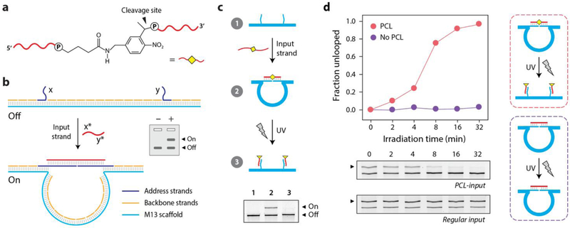
We have previously developed DNA nanoswitches, long DNA duplexes designed to reconfigure to form a loop in the presence of a target molecule.15 We and others have shown various applications including biosensing,16–18 biomolecular analysis,19 and single-molecule experimentation.15,20 We recently expanded its use in rewritable memory21 and graphical display of molecular events.22 Here we extend those concepts by using nucleic acid inputs that contain a photo-cleavable linker, enabling control of the outputs via light. To accomplish this, we employ oligonucleotides containing a photo-cleavable linker (PCL), which can be triggered to cleave by shining UV light (Figure 1a and Figure S1–2). We designed a DNA nanoswitch to respond to the PCL containing oligonucleotide, inducing a loop and causing a distinct shift of the DNA nanoswitch on an agarose gel (Figure 1b & Figure S3). When the input strand contains a photocleavable linker, the nanoswitches can be controlled by light, providing an external trigger to change the nanoswitches back to the linear off state (Figure 1c). Cleavage on UV exposure (λ=254 nm) severs the target strand in half, resulting in separation of the detectors, and thus unlooping (turning “off”) of the nanoswitch.
Figure 1. Photocleavable inputs and DNA nanoswitches.
(a) Chemical structure of the photocleavable linker incorporated into DNA strands. (b) DNA nanoswitches with target-specific detectors can bind DNA inputs changing from a linear off state to a looped on state. (c) An unlooped nanoswitch (1) can recognize its PCL-containing target and reconfigure to form a loop (2). Exposure to UV causes cleavage of the PCL target, causing the nanoswitch to return to its unlooped state (3). (d) Time series for UV exposure of unlooping nanoswitches. Control nanoswitches looped by a target strand without the photocleavable linker is not affected by UV exposure.
To characterize the kinetics of light-actuated conformational change (unlooping), we irradiated looped nanoswitches for varying lengths of time, and the unlooped fractions at each time point were quantified using agarose gel electrophoresis (Figure 1d). We observed that the looping efficiency of the nanoswitches was lower when a PCL was incorporated into our input strand (63% looping for regular input and 37% for PCL-input), likely due to interference of the PCL group which acts as an additional nucleotide in the middle of the sequence. We calculated the reduction in the looped fraction of nanoswitches compared to total nanoswitch population over irradiation time (higher unlooping is higher efficiency). Cleavage of the input strand (bound to the nanoswitch) increased over time with exposure to UV, eventually leading to complete unlooping of the nanoswitches in ~30 mins. As a control, we also irradiated nanoswitches that were looped by input strands that lacked photo-cleavable linkers to verify that the light induced reconfiguration was specific to photo-cleavage rather than a general effect of light irradiation such as heat generation. We observed no unlooping of the control nanoswitches (looped by target strands without PCL) even after 32 minutes of constant irradiation (Figure 1d). Together these results confirm that photocleavage proceeded as designed and can be used to restore the nanoswitches to their initial “off” state, with the conversion rate controlled by regulating irradiation dosage.
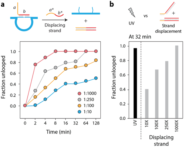
We then compared the UV-triggered unlooping of our nanoswitches to DNA strand displacement based reactions. We used a DNA strand containing an 8-nt toehold as input. Once looped, the nanoswitches can be reverted to their off state by adding a displacing strand that is fully complementary to the input strand (Figure 2a). We monitored release of input strand over time by quantifying the reduction in the looped band intensity (Figure S4). We also tested different concentrations of the displacing strands to analyze kinetics of the unlooping (input strand to displacing strand ratio of 1:10, 1:100, 1:250, 1:1000). Compared to UV-triggered unlooping at 32 mins, unlooping by DNA strand displacement is much slower, with only the 1:1000 ratio yielding an unlooped fraction similar to that obtained by UV (Figure 2b). Thus triggering such reactions using light is much faster, and avoids use of a large amount of material (micromolar quantities) compared to strand displacement.
Figure 2. DNA displacement versus UV-response.
(a) A nanoswitch looped by an input strand containing a toehold. The switch can be unlooped by the addition of a displacing strand that is fully complementary to the input. Plot shows kinetics of nanoswitch unlooping at different concentrations of the displacing strand. (b) Comparison of unlooped fractions at 32 minutes using UV and strand displacement.
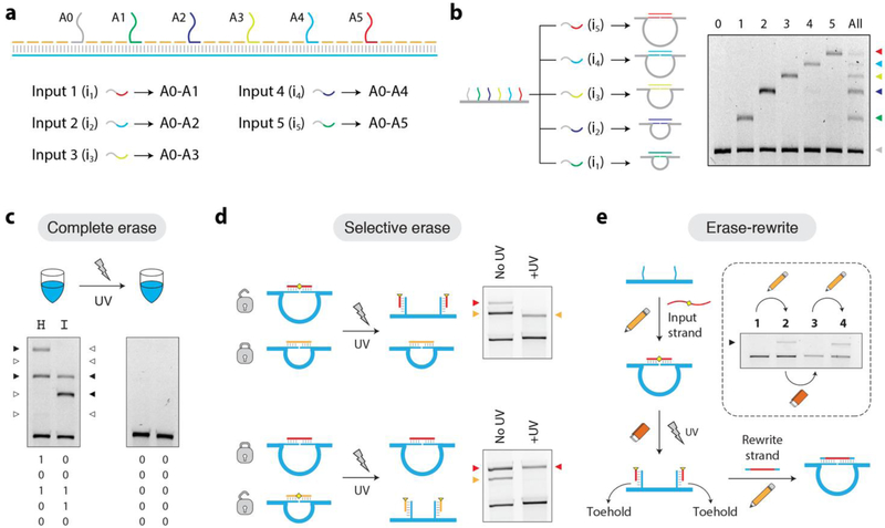
Following previous design strategies, we then extended the design of our nanoswitch to include multiple address site oligonucleotides so that the nanoswitch can be reconfigured in response to multiple DNA inputs.21 We incorporated six address strands (spaced ~600 base pairs apart) that can recognize five different input strands to form five unique loops (Figure 3a). Specific input strands cause the nanoswitches to reconfigure and form loops of different sizes corresponding to the distance between address sites (Figure 3b). All five input strands (or a subset) can be added to the nanoswitch triggering formation of multiple loops that are distinctly visible on a single gel lane. This forms a memory system that can encode 5 bits of information per gel lane, which can be translated into alphabet characters using the 5-bit Baudot code.23 By using PCL-containing target strands, bits can then be erased using light, destroying the encoded information and preventing re-reading (Figure 3c). We further demonstrate specific control over which of these bits can be erased. We added two inputs that trigger two different loops on the nanoswitch. By choosing which of these input strands contain the PCL, we can erase specific bit while the other remains (Figure 3d). In addition to writing and erasing capabilities, molecular memory systems also often require a rewriting functionality. To demonstrate the rewriting capability of this system once the bits are erased using UV, we used toehold-based DNA strand displacement (Figure 3e). When writing the bit, a 24-nt target strand binds to two 15-nt address sites, looping the nanoswitch. The 3-nt unhybridized region on each of the address site oligonucleotides can be used as a toehold (Figure S5). On exposure to UV, the target strand is cleaved resulting in unlooping, with 12-nt target fragments remaining on each of the detectors. We then added a rewrite strand that is complementary to the full length of the address site oligonucleotides (30-nt total). This strand binds to both toeholds and by double invasion of the duplex, displaces the fragments of the PCL input, resulting in reformation of the loop (Figure 3e, inset). Thus this system with UV-triggered inputs can be used for erasing while toehold design allows rewriting of erased bits. In this design, we incorporated a toehold on the detector strands. Recycling between erase and write processes is primarily limited by the number of toeholds. We have demonstrated multiple write-erase cycles (up to 8 cycles) in our earlier work where we designed a toehold on the input strand.21
Figure 3. Multi-input DNA nanoswitches and photo-response.
(a) A nanoswitch containing six address sites (A0–A5) that can recognize five different targets. (b) All target strands can bind to A0, but the second half binds to different address sites (0–1, 0–2, 0–3, 0–4, 0–5), leading to loops of different sizes that migrate differently on an agarose gel. (c) The word “HI” encoded using the 5-bit Baudot code by triggering different loops of the nanoswitch. The written information can be erased using UV. (d) Loops formed by PCL-containing inputs can be specifically erased among others. (e) Information (looped bits) erased using UV can be re-written using longer input strands through strand displacement.
Light-induced systems can be controlled in time and space, making photo-cleavable linkers useful tools in biological systems,24 not only for nucleic acids but also for peptides.25 Our system shows potential for the construction of light-responsive DNA memory, dynamic DNA nanostructures and DNA circuits. With the integration of photo-responsive elements, it is possible that DNA circuits (typically fueled by DNA)26 could show improved reaction rates. Our strategy is currently limited to UV by the nature of the PCL used in this study, though it does also respond to a wider UV range including 365 nm (UV-A) (Figure S6). Expansion to other wavelength-specific photoactive linkers1,27 could enable our DNA memory strategy to be addressable by light, for example controlling individual memory bits with different wavelengths of light. Further design tweaks could also enable switch-on control by light through photoreactive crosslinking, or reversible on/off switching through the use of reversible photoreactive molecules such as azobenzene.10,28 Another compelling possibility is expanding the range and complexity of inputs, for example integrating physical, chemical and biological control into DNA devices. Our strategy can also be extended to reconfiguration of other DNA nanostructures, potentially including dynamic DNA nanostructures that can be actuated via remote light triggers.
Supplementary Material
Acknowledgements
Research reported in this publication was supported by the NIH through NIGMS under award R35GM124720 to K.H. and R15GM124627 to J.S.
Footnotes
Electronic Supplementary Information (ESI) available: Methods and additional results. See DOI: 10.1039/x0xx00000x
Conflicts of interest
A.R.C. and K.H. are inventors on patents and patent applications covering aspects of the DNA nanoswitch design and applications.
References
- 1.Brieke C, Rohrbach F, Gottschalk A, Mayer G, Heckel A, Angew. Chem. Int. Ed 2012, 51, 8446–8476. [DOI] [PubMed] [Google Scholar]
- 2.Xavier PL, Chandrasekaran AR, Nanotechnology 2018, 29, 062001. [DOI] [PubMed] [Google Scholar]
- 3.Seeman NC, Sleiman HF, Nat. Rev. Mater 2018, 3, 17068. [Google Scholar]
- 4.Seeman N (2016). Structural DNA Nanotechnology. Cambridge: Cambridge University Press. [Google Scholar]
- 5.Krishnan Y, Simmel FC, Angew. Chem. Int. Ed 2011, 50, 3124–3156. [DOI] [PubMed] [Google Scholar]
- 6.Liang X, Nishioka H, Takenaka N, Asanuma H, ChemBioChem 2008, 9, 702–705. [DOI] [PubMed] [Google Scholar]
- 7.Kohman RE, Han X, Chem. Commun 2015, 51, 5747–5750. [DOI] [PMC free article] [PubMed] [Google Scholar]
- 8.Liu M, Jiang S, Loza O, Fahmi NE, Šulc P, Stephanopoulos N, N. Angew. Chem. Int. Ed 2018, 57, 9341–9345. [DOI] [PubMed] [Google Scholar]
- 9.Han D, Huang J, Zhu Z, Yuan Q, You M, Chen Y, Tan W, Chem. Commun 2011, 47, 4670–4672. [DOI] [PubMed] [Google Scholar]
- 10.Yang Y, Endo M, Hidaka K, Sugiyama H, J. Am. Chem. Soc 2012, 134, 20645–20653. [DOI] [PubMed] [Google Scholar]
- 11.Li F, Chen H, Pan J, Cha TG, Medintz IL, Choi JH, Chem. Commun 2016, 52, 8369–8372. [DOI] [PubMed] [Google Scholar]
- 12.Kohman RE, Cha SS, Man HY, Han X, Nano Lett. 2016, 16, 2781–2785. [DOI] [PMC free article] [PubMed] [Google Scholar]
- 13.Huang F, Liao WC, Sohn YS, Nechushtai R, Lu CH, Willner I, J. Am. Chem. Soc 2016, 138, 8936–8945. [DOI] [PubMed] [Google Scholar]
- 14.Takenaka T, Endo M, Suzuki Y, Yang Y, Emura T, Hidaka K, Kato T, Miyata T, Namba K, Sugiyama H, Chem. Eur. J 2014, 20, 14951–14954. [DOI] [PubMed] [Google Scholar]
- 15.Halvorsen K, Schaak D, Wong WP, Nanotechnology 2011, 22, 494005. [DOI] [PubMed] [Google Scholar]
- 16.Chandrasekaran AR, MacIsaac M, Dey P, Levchenko O, Zhou L, Andres M, Dey BK, Halvorsen K, Science Advances 2019, 5, eaau9443. [DOI] [PMC free article] [PubMed] [Google Scholar]
- 17.Chandrasekaran AR, Zavala J, Halvorsen K, ACS Sens. 2016, 1, 120–123. [Google Scholar]
- 18.Hansen CH, Yang D, Koussa MA, Wong WP, Proc. Natl. Acad. Sci 2017, 114, 10367–10372. [DOI] [PMC free article] [PubMed] [Google Scholar]
- 19.Koussa MA, Halvorsen K, Ward A, Wong WP, Nat. Meth 2015, 12,123–126. [DOI] [PMC free article] [PubMed] [Google Scholar]
- 20.Yang D, Ward A, Halvorsen K, Wong WP, Nat. Commun 2016, 7, 11026. [DOI] [PMC free article] [PubMed] [Google Scholar]
- 21.Chandrasekaran AR, Levchenko O, Patel DS, MacIsaac M, Halvorsen K, Nucleic Acids Res. 2017, 45, 11459–11465. [DOI] [PMC free article] [PubMed] [Google Scholar]
- 22.Chandrasekaran AR, ChemBioChem 2018, 19, 1018–1021. [DOI] [PubMed] [Google Scholar]
- 23.Ralston A and Reilly ED, (eds). (1993) ‘Baudot Code’, Encyclopedia of Computer Science, 3rd edn. IEEE Press/Van Nostrand Reinhold, NY, ISBN 0-442-27679-6. [Google Scholar]
- 24.Szymański W, Beierle JM, Kistemaker HAV, Velema WA, Feringa BL, Chem. Rev 2013, 113, 6114–6178. [DOI] [PubMed] [Google Scholar]
- 25.Rohrbach F, Schäfer F, Fichte MAH, Pfeiffer F, Müller J, Pötzsch B, Heckel A, Mayer G, Angew. Chem. Int. Ed 2013, 52, 11912–11915. [DOI] [PubMed] [Google Scholar]
- 26.Qian L, Winfree E, Science 2011, 332, 1196–1201. [DOI] [PubMed] [Google Scholar]
- 27.Lerch MM, Hansen MJ, Velema WA, Szymanski W, Feringa BL, Nat. Commun 2016, 7, 12054. [DOI] [PMC free article] [PubMed] [Google Scholar]
- 28.Gu R, Lamas J, Rastogi SK, Li X, Brittain W, Zauscher S, Colloids and Surfaces B: Biointerfaces 2015, 135, 126–132. [DOI] [PubMed] [Google Scholar]
Associated Data
This section collects any data citations, data availability statements, or supplementary materials included in this article.


