Abstract
This paper presents a pixel pitch-matched readout chip for 3-D photoacoustic (PA) imaging, featuring a dedicated signal conditioning and delta-sigma modulation integrated within a pixel area of 250 µm by 250 µm. The proof-of-concept receiver was implemented in an STMicroelectronics’s 28-nm Fully Depleted Silicon On Insulator technology, and interfaces to a 4 × 4 subarray of capacitive micromachined ultrasound transducers (CMUTs). The front-end signal conditioning in each pixel employs a coarse/fine gain tuning architecture to fulfill the 90-dB dynamic range requirement of the application. The employed delta-sigma beamforming architecture obviates the need for area-consuming Nyquist ADCs and thereby enables an efficient in-pixel A/D conversion. The per-pixel switched-capacitor ΔΣ modulator leverages slewing-dominated and area-optimized inverter-based amplifiers. It occupies only 1/4th of the pixel, and its area compares favorably with state-of-the-art designs that offer the same SNR and bandwidth. The modulator’s measured peak signal-to-noise-and-distortion ratio is 59.9 dB for a 10-MHz input bandwidth, and it consumes 6.65 mW from a 1-V supply. The overall subarray beamforming approach improves the area per channel by 7.4 times and the single-channel SNR by 8 dB compared to prior art with similar delay resolution and power dissipation. The functionality of the designed chip was evaluated within a PA imaging experiment, employing a flip-chip bonded 2-D CMUT array.
Index Terms: 3-D photoacoustic (PA) imaging, analog-to-digital conversion (ADC), capacitive micromachined ultrasound transducer (CMUT), CMOS, delta-sigma modulation, FDSOI, matrix transducer array, subarray beamforming, ultrasound (US)
I. Introduction
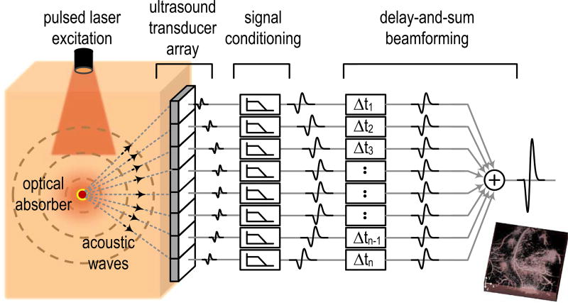
Photoacoustic (PA) imaging is an emerging medical imaging modality based on optical excitation and acoustic detection. As shown in Fig. 1, PA imagers employ a short laser pulse to illuminate a tissue sample. In regions with high absorption, the incident energy is converted to heat, leading to localized thermoelastic expansions and pressure waves that can be detected by an ultrasound (US) receiver (e.g., using standard US probes [1], [2]) outside the sample. This approach combines the sharp contrast of optical imaging and the low scattering of US to reveal detailed physiological tissue properties. PA imaging is therefore widely used in a variety of clinical research applications, such as the study of cancer progression [3].
Fig. 1.
Illustration of PA imaging.
This paper focuses on the design of the US readout electronics, with a specific emphasis on the dense integration of the signal conditioning and delay-and-sum (DAS) beamformer (BF) in Fig. 1. The most significant challenge that we address lies with the DAS operation, which requires small step size and wide delay range. The timing resolution of the required delay lines (Δt in Fig. 1) is inversely proportional to the carrier frequency [4], amounting to ~10 ns for the 5-MHz transducer center frequency used in this paper. On the other hand, the maximum delay is proportional to the array size. For example, a 100-element 1-D array requires a delay of 16 µs. Due to these requirements, it is most common to push the delays into the digital domain by placing an analog-to-digital converter (ADC) before the DAS block. The so-constructed commercial US systems typically employ 10–12 bit ADCs, running at >65 MS/s to provide both sufficient timing and signal resolution [5], [6]. Due to the ADC area and power overhead, the backend of the readout electronics is often separated from the probe head, and is connected to the transducer array using micro-coaxial cables.
While this solution is acceptable for current 2-D imagers with a 1-D transducer array (shown in Fig. 1), it is unsuitable for the next-generation systems that support 3-D volumetric imaging using 2-D transducer arrays with thousands of elements. To address this issue, prior work has already demonstrated the close integration of the transducer array and receive (RX) electronics using flip-chip bonding [7] or direct transducer integration [8]. The key idea in the latter approach is to perform local data reduction via subarray beamforming, which applies the DAS operation to a group of pixels. The final beamforming operation is then pushed off chip using a more manageable number of leads. For example, if the subarray beamforming is applied to a group of 16 pixels, the signal lead count is also reduced by a factor of 16. With the cable issue eliminated, the burden is now pushed onto the subarray beamforming electronics, which must be designed in a pixel pitch-matched style and within a very small per-channel area (250 µm × 250 µm in this paper). To meet these constraints, prior work has implemented the delays using sample and hold (S/H) circuits [8] or analog filters [9]. However, such analog approaches tend to sacrifice performance and typically suffer from a combination of issues related to restricted delay range, coarse delay resolution, and/or limited SNR.
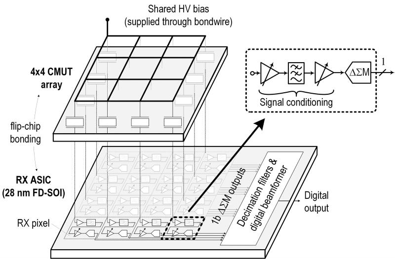
The goal of our work was to demonstrate the pixel pitch-matched integration of an ADC-based US receive-chain with on-chip digital subarray beamforming, specifically leveraging the immense integration density available in modern CMOS. Our proof-of-concept system was designed using an STMicroelectronics’s (ST’s) 28-nm Fully Depleted Silicon On Insulator (FD-SOI) technology and supports one single subarray of 4×4 pixels (see Fig. 2). The CMOS die is flip-chip bonded to a capacitive micromachined US transducer (CMUT) chip (similar to [7]).1 Each pixel contains inverter-based signal conditioning stages and an inverter-based delta-sigma modulator (ΔΣM), enabling a compact analog design with small passives (due to oversampling). Since the US path in PA imaging is RX only, a transmit interface is not integrated in this paper. However, in a large-scale array implementation, it is conceivable to add this functionality using a subset of the pixels for transmit, as done in [8].
Fig. 2.
Pixel-matched subarray BF ASIC with flip-chip bonded sensor.
The remainder of this paper expands the descriptions of our conference contribution [10] and is organized as follows. Section II describes the system architecture and the implementation of the digital subarray BF. Section III provides the circuit details of the pixel-size receiver, including the signal conditioning and the third-order single-bit ΔΣM. Section IV presents the experimental results, followed by conclusions in Section V.
II. System Architecture
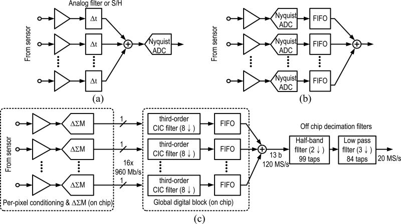
Fig. 3 compares the block diagrams of prior art and our system. Fig. 3(a) represents BF approaches using analog filters [9] or S/H circuits [8], [11]. Creating a time delay with an analog filter requires the approximation of a linear phase characteristic, which suffers from a strong tradeoff between filter bandwidth and maximum delay. For a bandwidth of 5–10 MHz, the delay of an analog filter is typically limited to a few nanoseconds, necessitating extensive cascading to achieve delays in the microsecond range. The S/H approach provides a longer delay up to ~1 µs [11], which is sufficient for a subarray. However, the S/H cells become large with increasing SNR due to kT/C noise requirements, limiting the number of delay cells for a given area. In addition to the accumulation of noise, previous work also reports SNR degradation due to charge injection and clock feedthrough errors in the memory cells [8]. Generally, from the results seen in the present literature, it is clear that making large delays with high SNR using analog blocks (such as filters or S/H stages) is challenging. For this reason, commercial US systems have converged toward the scheme in Fig. 3(b). Each channel of a 1-D array is digitized using a Nyquist ADC and the DAS operation is realized in the digital domain, yielding superior SNR, delay range, and programmability. However, as mentioned previously, it has been difficult to extend this scheme toward pitch-constrained 2-D arrays. In search of a solution, the work of [12] multiplexes a single ADC between eight channels to amortize the ADC area, but the result is a per-channel footprint that is approximately eight times larger than our pixel. Similarly, the work of [11] combines analog and digital Nyquist-rate BF, but still results in an area of approximately five times our pixel footprint.
Fig. 3.
(a) Analog BF. (b) Digital BF with Nyquist-rate ADCs. (c) Our system with ΔΣ BF.
To enable area-efficient digital BF, this work leverages ΔΣ approach [13]–[15] to perform DAS operations on the single-bit outputs of oversampling modulators [see Fig. 3(c)]. The oversampling of the ΔΣM naturally provides sufficient BF time resolution and further leverages the high sampling rate for noise shaping. This stands in contrast with Nyquist-based systems, where some undesired amount of oversampling is employed just to meet the required time granularity. For example, a timing resolution of 10 ns corresponds to a 100 MS/s Nyquist-based system, suggesting 5× over-design in sampling rate since the required signal bandwidth is merely 10 MHz. The shown three-stage ΔΣ BF is similar to [16] and was optimized for power and area. The first stage consists of a cascaded integrator comb (CIC) filter, followed by DAS and second- and third-stage decimation filters (DFs), which are shared within one subarray. Typically, the order of the CIC filter should be at least one order higher than that of the ΔΣM; however, the noise transfer function (NTF) of our modulator shows a second-order slope at high frequencies (>100 MHz), justifying the use of a third-order CIC filter in this paper. For the sake of simplicity, only the CIC filter and the DAS operation are implemented on chip, while the remaining (non-critical) operations are performed in software.
A known issue for ΔΣBF is the raised noise floor with dynamic (time varying) focusing, which causes omission or repetition of bits in the sequence and consequently disturbs the synchronization between the ΔΣMs and the decimation process. Dynamic focusing essentially generates frequency-dependent aliases and thereby causes out-of-band noise to leak into the signal band [17]. To avoid such bit distortion, we employ block-based ΔΣBF [18], [19], which represents a sample using a sequence of bit streams that are shifted as a complete block during dynamic focusing. Although the block-based ΔΣBF approach is more complex, it leads to higher fidelity images, which is crucial for medical applications.
Within the on-chip digital block [dashed box in the center of Fig. 3(c)], the BF is placed after the CIC filter as shown in Fig. 4(a), which was identified as the preferred option due to the lower FIFO clock speed and the commensurate reduction in power (see Table I). Conventional block-based ΔΣBF share a single CIC filter by performing bit-wise summation on blocks of data [18], [19] as shown in Fig. 4(b), which simplifies the adder (fewer bits) and leads to a smaller gate count. However, we found that the savings are insignificant due to the relatively low complexity of the CIC filter. The overall footprint and power is largely dominated by the shift registers (FIFO), which have similar sizes in both implementations, as they merely exchange bit width and throughput. The advantages of the DF first option are expected to become more pronounced for larger arrays, where early clock rate reduction is critical. To ensure sufficient timing resolution, the CIC filter has a decimation factor of 8, providing an output rate of 120 MS/s. The implemented FIFOs have a depth of 27, supporting the maximum timing delay (~940 ns) across the diagonal of our 4×4 subarray with ~10% margin.
Fig. 4.
Comparison of two ΔΣBF implementations. (a) DF first. (b) BF first.
TABLE I.
Gate Counts and Power Comparison for ΔΣBF
| Gate Count | BF first | DF first | Power [mW] | BF first | DF first |
|---|---|---|---|---|---|
| adder | 43 | 434 | adder | 0.08 | 0.09 |
| DF | 372 | 4624 | DF | 0.46 | 5.18 |
| FIFO + MUX | 77,296 | 78,144 | FIFO + MUX | 160 | 89.6 |
| Total | 77,711 | 83,202 | Total | 160.5 | 94.9 |
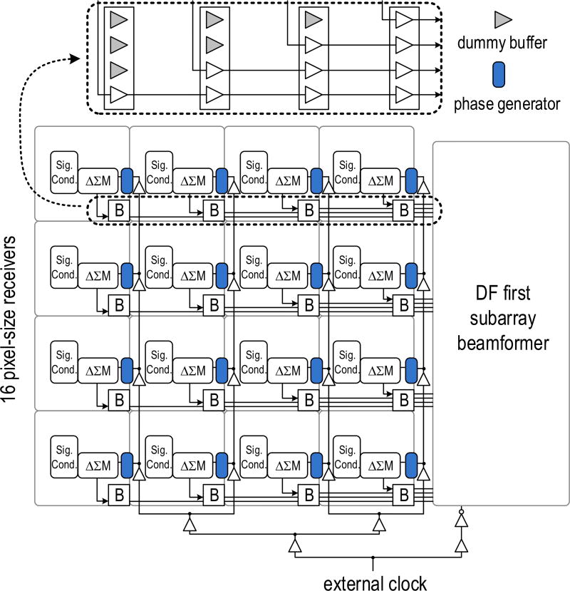
Fig. 5 shows the floor plan of the overall system, in which the 16 pixel-size receivers are aligned in a 4 × 4 grid and abutted with the synthesized global digital block. A global clock of 960 MHz is provided externally and distributed to the digital block and the pixel-size receivers. The non-overlapping clock phases for the contained switched-capacitor (SC) circuits are generated locally to manage delay and clock skew, thereby relaxing the matching requirements on the global clock network. The output bitstream from each channel is routed to the digital block with distributed buffers, which are sized to meet the setup/hold time requirement at the input of the digital block. For this design, no data and clock recovery are needed in the DF and BF block since the delay from the single-bit output of the modulators is small. For large array implementation, D-flip-flops can be inserted into the path to ensure well-defined data propagation. As indicated in Fig. 5, four buffer cells are required in each pixel for a 4×4 array. Thanks to the employed fine-line process, the area and power of the distributed buffers is insignificant compared to the pixel circuitry. Compared to the implementation of analog BF or digital BF using Nyquist ADCs, the number of required distributed buffers is much reduced due to the single-bit ΔΣM, which not only preserves signal integrity, but also simplifies the task of combining the signals in a global digital block outside the array. More importantly, the pitch-matched implementation of the receiver blocks will allow for a relatively straightforward extension to a large array.
Fig. 5.
System floor plan with data path and clock distribution (area not drawn to scale).
III. Pixel-Size Receiver
As shown in Fig. 2, both the signal conditioning circuits and the ΔΣM are embedded inside the pixel-size receiver. Their specifications are determined by the signal characteristics. When acoustic waves and light propagate through the tissue, the signal suffers from energy loss due to scattering and absorption, leading to depth-dependent attenuation. For acoustic waves, the attenuation due to absorption is ~1 dB/cm/MHz for most soft tissues [20]. On the other hand, the optical properties vary among tissues; in general, the attenuation and scattering of light are more severe than those of acoustic waves, limiting the imaging depth to few centimeters in clinical trials [21]. In order to compensate the depth-dependent attenuation, the front-end gain is increased with time, commonly known as time-gain control in US system. In this paper, a 30-dB variable gain is designed for an imaging depth of around 2 cm [22]. At 1-cm depth, the laser-induced pressure signal received by the sensor is of the order of a few kilopascals,2 largely depending on the absorption coefficient of the target and surrounding media. On the other hand, the noise floor of the transducer is around a few pascals [22]; therefore, the instantaneous dynamic range (DR) (essentially the SNR of the ΔΣM) is designed for ~60 dB. Together with 30-dB variable gain, this leads to an overall input DR of 90 dB. Besides the area-demanding ΔΣM, both the high DR and variable gain range impose challenges for the signal conditioning design within the pixel area. Dedicated circuit techniques are applied to meet these requirements, as discussed in this section.
A. Signal Conditioning
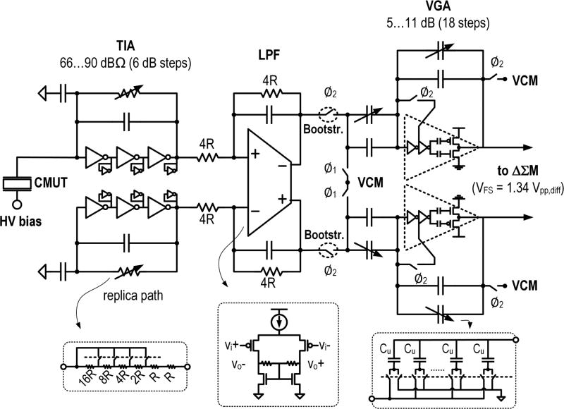
Fig. 6 shows the schematic of the signal conditioning circuit, which includes a preamplifier, low-pass filter (LPF), and variable gain amplifier (VGA). To cover the wide variable gain, the tuning range is distributed among the preamplifier and the VGA based on a coarse and fine gain structure. The preamplifier is a transimpedance amplifier (TIA) that converts the current generated from the CMUT into a voltage using five different gain levels (6-dB steps). The TIA output is taken against a replica circuit to facilitate supply-noise cancellation as the succeeding LPF performs single-ended to differential conversion. While device variability affects the operating point voltage and inter-channel offset at the TIA input, this has a little impact due to the relatively large bias voltage (20 … 30 V) across the CMUT and the bandpass nature of the desired signal. In order to perform single-ended to differential conversion, the LPF, implemented as an active RC filter, needs to have good common-mode (CM) rejection, and therefore uses a single-stage fully differential amplifier with resistive load as shown in Fig. 6. The CM feedback is implemented using a self-biased diode connection for its simplicity [23]. Both the TIA and LPF are designed using 1.5-V-thick oxide devices (for large DR), while all other circuits use core devices with a 1-V supply. The VGA uses a Padé approximation [24] to provide a fine linear-in-dB gain tuning (5–11 dB in 18 steps) to ensure signal continuity during gain transitions. It is implemented using an SC approach and is designed with a slightly extended gain range to compensate for gain errors due to process variations and non-idealities, as for instance the finite on resistance of the switches and finite loop gain in the TIA. Both the TIA and SC VGA are pseudo-differential and employ inverter-based amplifiers to achieve a compact design.
Fig. 6.
Circuit implementation of the signal conditioning circuit inside a single pixel.
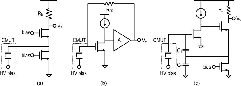
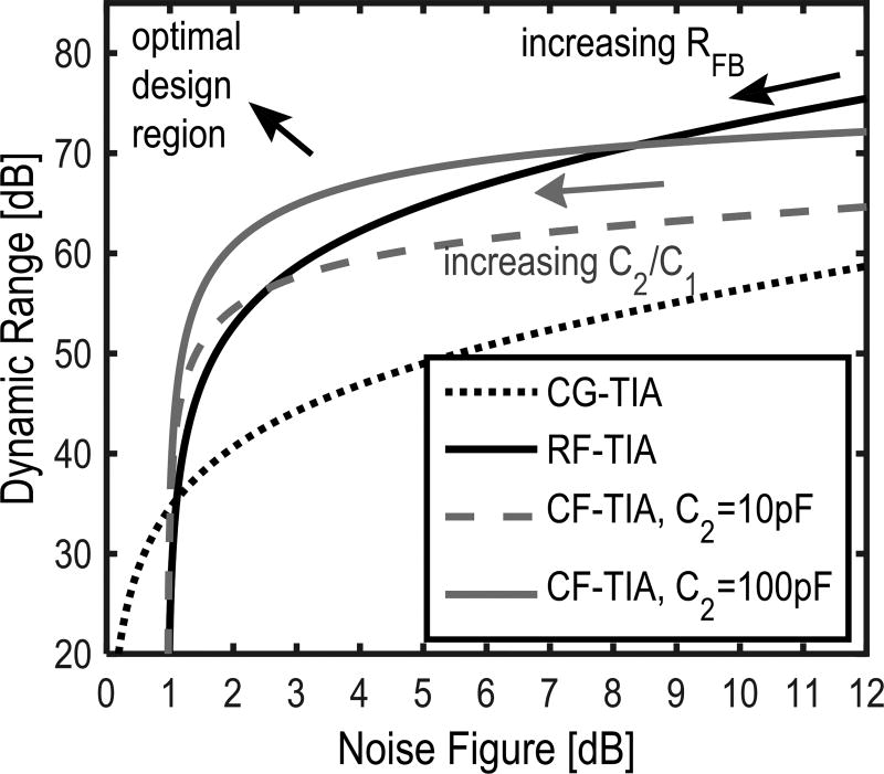
The TIA is optimized for DR and noise figure (NF). Fig. 7 shows several popular TIA architectures: common gate (CG), resistive feedback (RF), and capacitive feedback (CF). A higher TIA gain improves the NF at the expense of reduced input current, causing degradation in the DR due to output swing constraints. Fig. 8 illustrates the tradeoff for these three architectures quantitatively (see [22] for further details), assuming that the CMUT contributes an equivalent noise of a 68-kΩ resistor at the source with a 5-MHz center frequency. The CF TIA outperforms the other two options since the current amplifying stage formed by C1 and C2 does not contribute noise and attenuates the noise of RL [25]. However, the area required by C2 grows significantly and becomes unrealizable under the pixel area constrains. Therefore, the RF TIA was considered as the best choice for this work. Nevertheless, to maintain an input DR of 90 dB, a resistive TIA with fixed gain leads to a poor NF performance (>12 dB, outside the range of Fig. 8) due to the reduced voltage swing imposed by our fine-line CMOS process. With variable TIA gain control, the instantaneous DR of the TIA is reduced to 66 dB, avoiding significant NF degradation. The resultant (simulated) NF of the analog front end is 7.8 dB at the highest gain setting (32 kΩ) of the TIA. The inverter-based amplifier of the TIA has the dominant pole at the input and relies on the compensation effect of the gm load and the feedback zero to achieve stability.
Fig. 7.
Transimpedance amplifier architectures. (a) Common gate. (b) Resistive feedback. (c) Capacitive feedback (dc biasing for C1/C2 not shown).
Fig. 8.
DR versus NF for different transimpedance amplifier architectures.
B. Delta-Sigma Modulator
Fig. 9 shows the block diagram of the single-bit, discrete-time ΔΣ architecture [26] used in this work. The coefficients of the loop filter are well defined by capacitor ratios. Besides, it benefits from the oversampling ratio and the noise shaping, making the architecture less sensitive to process variation. The ΔΣM features a third-order NTF to achieve 60-dB peak signal-to-noise-and-distortion ratio (SNDR) over a 10-MHz signal bandwidth with an oversampling ratio (OSR) of 48. The sampling rate is 960 MHz. Additional feed-forward paths relax the output swing and slew rate requirements in the first and second integrators [27]. The signal transfer function (STF) and NTF of this architecture are expressed as
| (1) |
| (2) |
Fig. 9.
Block diagram of the discrete-time ΔΣM.
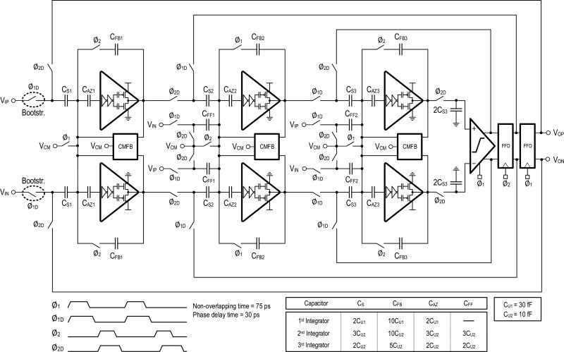
Fig. 10 shows the complete pseudo-differential implementation of the modulator with its clock phases [28]. The circuit uses a conventional discrete-time common-mode feedback [26], not shown in the figure. To maximize the signal DR, the input and output common-mode voltages are set to mid-rail. The size of the sampling capacitors is determined by the thermal noise requirement, which for this design amounts to 75% of the total noise budget. The sampling capacitance of the first and second integrators can be estimated using a similar approach as presented in [29]
| (3) |
| (4) |
k = 1.38 × 10⁻²³ J/K is Boltzmann’s constant, T is the absolute temperature in Kelvin, and is the total noise budget at the given resolution and full-scale input. Ron1 and Ron2 are the on resistance of the switches in the first and the second integrators. The noise contribution of the third integrator is negligible due to the second-order noise shaping of its input signal. For each of the integrators, the amplifier noise is dominated by the first stage inverter, and its transconductance (gm1, gm2) is optimized for both power and noise. Equations (6) and (7) include an additional design parameter Pn, which represents the fraction of noise from the first integrator. With Pn = 78.8%, (6) and (7) achieve their lowest value, minimizing the total capacitance area required by the modulator. For this design, CS1 = 60 fF and CS2 = 30 fF, which includes some design margin to mitigate the impact of wiring parasitics. As illustrated in Fig. 10, unit capacitors CU1 = 30 fF and CU2 = 10 fF set the coefficients of the modulator. A double-tail latch-type voltage sense amplifier similar to [30] is used as the comparator. It enables a fast response to support the chosen sampling frequency (960 MHz) and is well suited for 1-V operation.
Fig. 10.
Circuit implementation of the discrete-time ΔΣM.
C. Inverter-Based Amplifiers
The amplifier blocks of the SC ΔΣM and VGA rely on inverter-based topologies, which have gained increasing attention in fine-line CMOS due to their compactness and low-voltage compatibility. A variety of inverter-based amplifiers have been proposed to implement active elements in high-performance, power-efficient ADCs. Chae and Han [26] introduce a single-inverter structure for a discrete-time modulator. The inverter can operate as a class-AB or class-C stage when operated at the boundary between weak and strong inversion. This amplifier provides a power-efficient solution; however, the voltage gain of a single inverter is usually small, preventing the use of minimum-length devices. The amplifier in [31] enhances the gain using a three-stage architecture using single-ended common source stages, but is relatively inefficient due to class-A operation. The ring amplifier [32] represents an interesting alternative for SC circuits. It is created by splitting a ring oscillator into two paths and embedding different offsets in each path to preserve the bias condition of the last stage. This architecture enables a high gain through the cascade of three stages and at the same time reaps the benefits of efficient slew-based charging with inherent rail-to-rail output swing. A modified version of the ring amplifier was introduced in [33]. It reduces the number of inverters in the second stage and eliminates the external biases; however, it employs high VT devices in the last stage to extend the stable offset range and relies on a resistor to define the bias point of the output transistors.
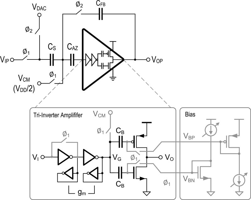
In this paper, a different variant of a power- and area-efficient inverter-based amplifier was developed. Fig. 11 shows its half-circuit (the full circuit is pseudo-differential), along with the integrator in which it is utilized. Similar to the aforementioned solutions, it employs three gain stages to achieve large voltage gain with minimum gate length, and it is designed to slew for most of the clock period. The large swing at the third stage input during slewing leads to small devices and a compact layout. As illustrated in Fig. 11, the input signal is sampled onto CS with respect to the self-bias voltage of the first inverter during ϕ1. At the same time, the input bias of the third stage is established using diode replicas and stored on CB. In comparison with [33], this obviates the need for special high VT devices and resistors. The currents for the N/P diode replicas originate from the same current reference, providing the same bias current at default. For testing and experimental purpose, they are made independently adjustable; no calibration is performed on individual channel during operation. During ϕ2, the charge is redistributed between CS and CFB to perform integration. The auto-zeroing capacitor3 CAZ suppresses the amplifier’s offset and flicker noise [34]. A similar clock sequence is used within the SC VGA of Fig. 6.
Fig. 11.
Half-circuit of the pseudo-differential SC integrator with tri-inverter amplifier and bias circuit.
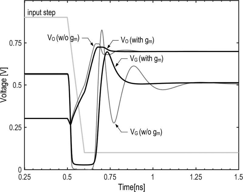
Near the end of the settling process, the employed tri-inverter amplifier exhibits the characteristics of a third-order linear system. To ensure that the loop stabilizes after slewing, the settling performance of the amplifier is optimized based on its open-loop damping factor [35], which for this design is set to about one [22]. To adjust the damping, the tri-inverter amplifier contains gm loads at the output of the first two inverters (see Fig. 11). These compensation devices are ratiometrically defined using scaled versions of the main inverters, and are thus insensitive to process variation. The effectiveness of the added gm is illustrated in Fig. 12. This plot compares the transients of the last stage’s input and output (VG and VO) with and without compensation and illustrates the fast settling with the gm compensation present. A larger gm load improves stability by pushing the nondominant poles at the outputs of the first and the second stages to a higher frequency while reducing the loop gain and hence loop gain-bandwidth product [22]. As a final detail, note that the internal VG node overshoots significantly, even with gm compensation. In a bulk CMOS process and for very large signals, this could lead to a forward-bias condition for the switch junctions. However, in the employed FD-SOI process, this was not a concern due to the oxide-isolated junctions.
Fig. 12.
Simulated transient signals of the tri-inverter amplifier with and without gm compensation.
IV. Experimental Results
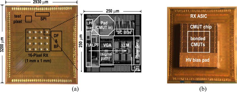
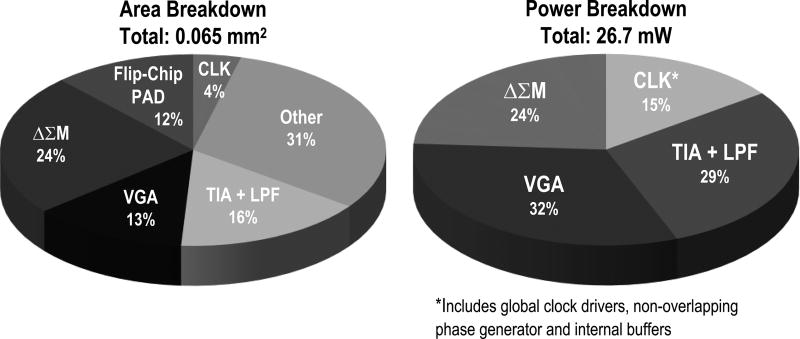
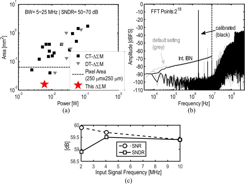
The 4 × 4 US receiver prototype was fabricated in ST’s 28-nm Ultra-Thin Body and Buried oxide FD-SOI process. Fig. 13(a) shows the die micrograph, including the floor plan of a single pixel. Fig. 13(b) depicts the chip stack, in which a diced 4 × 4 2-D CMUT array is flip-chip bonded (same approach as in [7]) onto the 28-nm chip. Besides the 16 RX pixel array, an additional test pixel is used to separately evaluate the performance of the TIA-LPF and the SC VGA-ΔΣM cascades. The test structure has the same layout as the functional pixel, but with the signal path between the LPF and the SC VGA disconnected. The 16 RX pixels occupy 1 mm2 and consume 358 mW, while the synthesized digital block occupies 0.4 mm2 and consumes 173 mW. The ΔΣM occupies 1/4th of the pixel area and consumes 6.65 mW. The power and area breakdown of a single pixel are shown in Fig. 14. The designed ΔΣM is the smallest published among designs with similar BW and SNDR, as shown in Fig. 15(a).
Fig. 13.
(a) Die microphotograph including layout of a single pixel. (b) Chip stack with CMUT.
Fig. 14.
Area and power breakdown of a single-channel pixel-size receiver.
Fig. 15.
(a) State-of-the-art comparison (area versus power) for ΔΣM. (b) Measured output spectrum of the isolated SC VGA-ΔΣM cascade in the test pixel. (c) SNR and SNDR across input frequency.
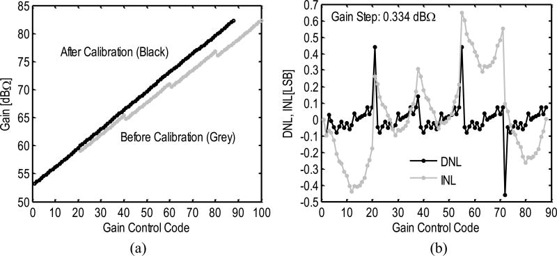
Fig. 15(b) shows the measured output spectrum of the VGA-ΔΣM test structure (with the entire chip in full operation), achieving SNRpeak = 59.9 dB and SNDRpeak = 58.9 dB for a 2-MHz input sinusoid, while Fig. 15(c) shows that this performance is maintained up to fin = 10 MHz. Fig. 16(a) shows the gain sweep of a complete pixel, achieving a variable gain range of 29.1 dB with 0.33 dB steps, which are close to the given specifications. A control code sequence is selected from the default gain sweep (gray) to produce the calibrated output curve (black). The default gain sweep is performed for individual channels by measuring the output signal amplitude with a fixed-amplitude input sinusoid under different control code settings. As shown in Fig. 16(b), the differential nonlinearity (DNL) and integral nonlinearity (INL) after foreground calibration are within 0.46 LSB and 0.65 LSB, respectively. Unfortunately, gain degradation was observed in the measurement of the full signal chain due to a chip fabrication issue, which created a low-impedance load at the output of the LPF, hindering the circuit to operate at the designed bias condition. The measured SNDRpeak of a complete pixel is thus degraded to 41.9 dB from the simulated value of 58 dB after post-layout. Nevertheless, using the highest gain setting for each pixel still led to satisfactory imaging results and overall system validation as described in the following.
Fig. 16.
(a) Measured gain sweep of a complete pixel. (b) Measured DNL and INL of the calibrated gain profile.
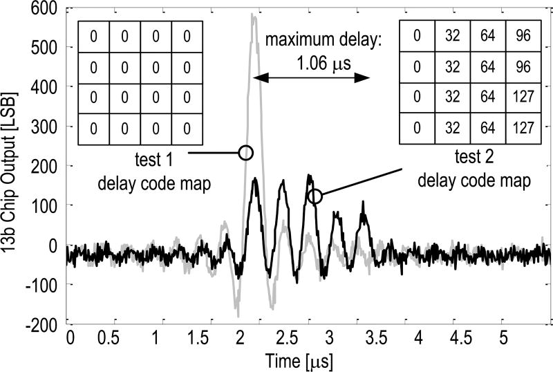
To evaluate the functionality of the full chip, the 13-bit BF output is measured with different delay code configurations stored in on-chip programmable memory, while a synchronized sinc-like current pulse is injected into the array from a function generator. Fig. 17 shows the two different delay code configurations and the corresponding output results. In the first test, a single pulse is measured at the BF output since all channels receive the same delay code. The measurement of the second test shows five pulses, corresponding to the five different delay codes that were applied (see test 2 delay code map). The fourth and fifth pulses are halved in amplitude since only two (instead of four) elements are summed with these delays. The maximum delay supported in this paper is 1.06 µs as illustrated by the distance between the first and the fifth pulses in the second test.
Fig. 17.
Measured BF output with different delay configurations.
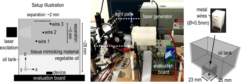
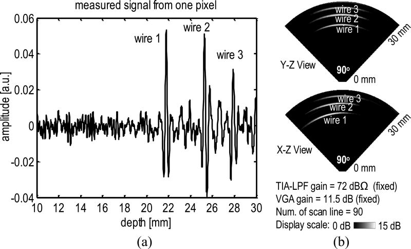
The receiver was also tested within a PA imaging setup, where the acoustic signals are induced by laser pulses as illustrated in Fig. 18. The device is mounted on an evaluation board and immersed in an oil tank for acoustic coupling. A laser pulse (λ = 740 nm) is applied from the side of the oil tank, providing an average fluence of 20 mJ/cm2 with a 10-ns pulsewidth and pulse repetition rate of 10 Hz. A phantom with three embedded metal wires is inserted into the lower part of the oil tank, whose shape is designed to accommodate other components on the evaluation board. The signal processed by the silicon chip assembly is captured by a logic analyzer and averaged 30 times for each image data point to compensate the SNR degradation in the conditioning circuit (caused by a fabrication issue). Both the laser and the logic analyzer are triggered by the same pulse signal for synchronization. Fig. 19(a) shows the measured raw data captured from one pixel, while Fig. 19(b) shows the reconstructed image with dynamic focusing. The cross-sectional view from the yz plane shows three parallel wires at different depths, while the view from the xz plane captures their diagonal placement. The spreading of the image in the xz plane is due to the small subarray size in this design.
Fig. 18.
Experimental setup for the PA imaging.
Fig. 19.
(a) Measured raw data from a single pixel. (b) Measured image of the three wire targets.
Table II compares this work to the state of the art. Since the signal conditioning circuit differs from the designed specifications due to the chip fabrication issue, this comparison mainly focuses on the BF performance, which considers only the ΔΣM and digital blocks. Relative to the hybrid analog/digital BF approach of [11], this paper has comparable delay resolution and power dissipation, while achieving 7.4 times smaller area and 8-dB improvement in a single-channel SNR. The maximum delay range is lower due to the different requirements imposed by the 4 × 4 array, but it can be extended through a longer FIFO. More recent work using a nonuniform sampling approach [36] demonstrates similar performance as the hybrid design while dissipating 50% less power, showing the advantage of a fully digital BF approach. Compared to [36], our work consumes more power due to a much higher SNR target for PA applications. A direct comparison to the analog BF ICs [8], [9] is more difficult to make, due to the significantly different performance parameters. If the SNR and delay range are reduced to 40 dB and 200 ns, respectively, the power of the ΔΣM and BF is reduced by approximately eight times and five times. This would yield a BF power of 2.99-mW/channel, which lies between the values seen for [8] and [9]. It is worth noting that the power consumption of the S/H BF [8] is an order of magnitude lower than our projection for a reduced-SNR version of our approach, highlighting the power efficiency of analog approach when the SNR requirement is less demanding.
TABLE II.
Comparison With the State of the Art
| This Work | VLSI’16 [8] | TBCAS’12 [9] | ISSCC’14 [11] | TBCAS’17 [36] | |
|---|---|---|---|---|---|
| Transducer Type | 2D CMUT | 2D PZT | Annular CMUT | 2D CMUT | 2D |
| Center Frequency | 5 MHz | 5 MHz | 40 MHz | 3 MHz | 5 MHz |
| RX BF Domain | Digital | Analog | Analog | Hybrid | Digital |
| Delay Cell | ADC+FIFO | S/H | Analog Filter | S/H+ADC+FIFO | ADC+FIFO |
| Technology | 28 nm | 180 nm | 350 nm | 130 nm | 130 nm |
| No. of Channels | 16 | 864 | 8 | 64 | 64 |
| Channel Reduction | 16 fold | 9 fold | 8 fold | 64 fold | 64 fold |
| Integration Method | Flip-chip | Chip integr. | Wire bonding | Wire bonding | Wire bonding |
| Pitch-matched | Yes (250 µm) | Yes (150 µm) | No | No | No |
| Max. Delay [µs] | 1.067 | 0.21 | 0.035 | 8 | 7.875 |
| Delay Resolution [ns] | 8.33 | 30 | 1.75~2.5 | 6.25 | 6.25 |
| BF Area/Channel [mm2] | 0.041 | †0.023 | 0.045 | 0.303 | †0.4727 |
| BF Power/Channel [mW] | 17.5 | †0.27 | 4.625 | 17.8125 | †9.4531 |
| *BF peak SNR/Channel [dB] | 59.9 (set by ΔΣM) | †< 40 (estimation) | 32~42 | <53 (estimation) | †<50 (estimation) |
BF peak SNR/channel is the SNR of a single channel without beamforming gain
Includes LNA and TGC
To extend this work to a large array, it will be necessary to work on further power reductions. Based on the first results from digital synthesis, a 20% reduction could be achieved by replacing the low threshold voltage devices in the digital block with regular threshold voltage devices. To improve the power efficiency of the tri-inverter amplifier, a diode connected transistor could be added to the first inverter stage, lowering the effective power supply voltage [33]. Furthermore, as described in [37], a power-down mode can be added to the inverter-based amplifier. The small parasitics of the internal nodes allow fast transitions between during on–off power cycling. For a PA system, the imaging speed is often limited by the laser pulse repetition rate, which is around 10 Hz for the high-power nanosecond laser used in our basic laboratory experiment. Low-power nanosecond lasers support a higher repetition rate in the range of few kHz. While the selection of nanosecond lasers depends on application and imaging depth, the signal period of interest (e.g., ~32 µs for a 5-cm-deep image) is usually about 10× to 1000× smaller than the repetition period, implying a potential for over an order of magnitude power reduction for a duty-cycled system.
V. Conclusion
We presented the first proof-of-concept, pixel pitch-matched subarray BF IC for future 3-D PA imaging systems. Digital beamforming is enabled by employing a ΔΣBF architecture, which substitutes Nyquist ADCs with ΔΣMs and provides both fine delay resolution (<10 ns) and large (~1 µs) delay range. Dedicated signal conditioning circuits and ΔΣ modulators are optimized for both area and performance. The preamplifier and the VGA realize a coarse/fine gain tuning architecture to accommodate the large-signal DR as well as the wide variable gain required by the application. By using inverters as the main amplifiers and operating them mostly in the slewing regime, the designed SC ΔΣM achieves the smallest area among published works with similar bandwidth and SNDR. Although the overall signal conditioning circuit fails to meet the designed performance, the demonstration of in-pixel A/D conversion and efficient ΔΣBF are considered as the most important aspects of this paper. The presented approach demonstrates the potential for larger arrays with pitch-matched electronics, high-fidelity readout, and digital subarray BF in fine-line CMOS technologies.
Acknowledgments
The authors would like to thank STMicroelectronics through CMP for providing silicon fabrication. They would also like to thank R. Feuillette, C. Bernicot (ST), and J.-F. Paillotin (CMP) for design support, A. Tomada (SLAC), PacTech, and H. Nguyen (Silitronics) for chip assembly, and Prof. Khuri-Yakub, A. Bhuyan, B.-C. Lee, and J.-H. Jang for discussion and preparation of CMUT.
This work was supported in part by the Stanford’s Initiative on Rethinking Analog Design and the C2S2 Focus Center, one of the six research centers funded under the Focus Center Research Program, an SRC subsidiary. The work of S.-R. Kothapalli was supported under Grant NIBIB-K99EB017729.
Biographies

Man-Chia Chen (S’10–M’16) received the B.S.E.E. degree in electrical engineering from National Chiao-Tung University, Hsinchu, Taiwan, in 2008, and the M.S. and Ph.D. degrees in electrical engineering from Stanford University, Stanford, CA, USA, in 2011 and 2016, respectively. Her Ph.D. research focused on the design of portable 3-D medical ultrasound receivers in a 28-nm FD-SOI CMOS technology.
Since 2016, she has been a Mixed-Signal Circuit Designer with Bosch Sensortec, Palo Alto, CA, USA. Her current research interests include mixed-signal integrated circuit design and sensor interfaces.
Dr. Chen is a member of the Solid-State Circuits Society. She received the Pan Wen-Yuan Foundation Scholarship from Stanford University in 2012.
Aldo Peña Perez (M’10) received the B.S. degree in electronics engineering from the Technological Institute of Queretaro, Queretaro, Mexico, in 2004, the M.S. degree in microelectronics from the National Institute of Astrophysics, Optics and Electronics, Puebla, Mexico, in 2006, and the Ph.D. degree in microelectronics from the University of Pavia, Pavia, Italy, in 2010.
From 2010 to 2011, he was a Post-Doctoral Research Fellow with the Integrated MicroSystems Laboratory, University of Pavia. During his post-doctoral activity, he designed low-power and low-noise sensor interfaces for label-free DNA detection. From 2012 to 2013, he was an Analog Design Engineer with the Automotive Power Group, STMicroelectronics, Milan, Italy, where he developed data converter interfaces for low-voltage digital input quad-bridge class-D power amplifiers. From 2013 to 2015, he joined the Murmann Mixed-Signal Group, Stanford University, Stanford, CA, USA, as a Post-Doctoral Research Fellow, where he was involved in the design of a portable 3-D medical ultrasound receiver in a 28-nm FD-SOI CMOS technology and the implementation of low noise electronic transducers for nano-electrochemical sensing systems used for label- and probe-free detection of biological molecules. From 2015 to 2016, he was with the Microcontroller Division, Atmel Corporation, San Jose, CA, USA, as a Senior Analog Design Engineer, where he was involved mainly in the design of low power data converters. Since 2016, he has been an ASIC Design Engineer with the TID AIR Integrated Circuits Department, SLAC National Accelerator Laboratory, Menlo Park, CA, USA, where he is currently involved in the design of low-noise current readout ASICs operating at cryogenic temperatures. He has authored and co-authored over 25 technical papers including international journals and conference proceedings.
Dr. Perez is member of the Solid-State Circuits Society. He currently serves as a Reviewer of the IEEE Journal of Solid State Circuits, IEEE Transactions on Circuits and Systems—I: Regular Papers and IEEE Transactions on Circuits and Systems—II: Express Briefs, and IET Circuits, Devices and Systems.

Sri-Rajasekhar Kothapalli received basic education and research training in physics and optical engineering from IIT Delhi, New Delhi, India, and the Ph.D. degree in biomedical engineering from Washington University in St. Louis, St. Louis, MO, USA, in 2009. His Ph.D. thesis focused on ultrasound-modulated optical microscopy.
From 2009 to 2014, he held a post-doctoral position at Stanford University, Stanford, CA, USA, where he invented a transrectal ultrasound and photoacoustic (TRUSPA) imaging device for human prostate imaging. His notable inventions during this period include Cerenkov luminescence endoscopy and single cell photonic nanocavity probes. From 2014 to 2016, he was a Junior Faculty (Instructor) Member with the Department of Radiology, Stanford University. During this period, he translated the TRUSPA imaging system to clinic and conducted first-in-man prostate imaging on several patients using the TRUSPA device. Since 2017, he has been an Assistant Professor with the Department of Biomedical Engineering and Hershey Cancer Institute, Pennsylvania State University, State College, PA, USA. His research laboratory is focused on developing novel optical, ultrasound, and photoacoustic imaging/sensing principles and technologies for both preclinical and clinical applications in cancer and neurological diseases.
Dr. Kothapalli received the K99-R00 Pathway to Independence Grant Award from the National Institutes of Health to develop next-generation TRUSPA devices in 2014.

Philippe Cathelin received the Microelectronics Engineer degree from the Ecole Superieure d’Ingenieurs en Electrotechnique et Electronique, Marne-La Vallee, France, in 1989.
He first joined Mixed Silicon Structures, Roubaix, France, where he was involved in low power low voltage communication circuits. In 1997, he joined the Wireless Division, STMicroelectronics, Grenoble, France, where he designed RF BiCMOS transmitters for different cellular standards. In 2005, he joined ST-Ericsson, Crolles, France, where he was involved in implementing RF transceivers in CMOS. He returned back to STMicroelectronics research and development organization, where he has been involved in advanced CMOS mmW design activities since 2012. He also supervises Ph.D. students in the field of reconfigurable radio circuits.

Andreia Cathelin (M’04–SM’11) started electrical engineering studies at the Polytechnic Institute of Bucarest, Romania and graduated with engineering degree and MS from the Institut Supérieur d’Electronique du Nord (ISEN), Lille, France in 1994. In 1998 and 2013 respectively, she received PhD and “habilitation à diriger des recherches” (French highest academic degree) from the Université de Lille 1, France.
Since 1998, she has been with STMicroelectronics, Crolles, France, now Fellow in Digital Front-End Manufacturing & Technology. Her major fields of interest are in the design of RF/mmW/THz and ultra-low-power circuits and systems. Andreia has had numerous responsibilities inside the IEEE community since more than 10 years. At ISSCC, she has been the RF sub-committee chair from 2012 to 2015, and since 2016 is the Forums Chair and member of the Executive Committee. She is member of ESSCIRC TPC since 2005. Since September 2013, Andreia is on the Steering Committee of ESSCIRC-ESSDERC conferences, where she has been the Chair from 2015 to September 2017. During her mandate as ESSCIRC Steering Committee Chair, two major MoU’s have been signed with respectively SSCS and EDS societies, bringing now both conferences among the top ranked conferences in the respective fields, as financially fully sponsored events. She has served different positions on the Technical Program Committees of VLSI Symposium on Circuits from 2010 till 2016. She has been Guest Editor of the IEEE JSSC Special Issue on VLSI Symposium in April 2016.
Andreia has authored or co-authored 130+ technical papers and 7 book chapters, and has filed more than 25 patents. Andreia is a co-recipient of the ISSCC 2012 Jan Van Vessem Award for Outstanding European Paper and of the ISSCC 2013 Jack Kilby Award for Outstanding Student Paper; as well as winner of the 2012 STMicroelectronics Technology Council Innovation Prize.
She is an elected member of the IEEE SSCS Adcom for the term January 2015 to December 2017, and an active member of the IEEE SSCS Women in Circuits group.

Sanjiv Sam Gambhir received the B.S. degree in physics from Arizona State University, Tempe, AZ, USA, and the combined M.D.–Ph.D. degrees in biomathematics from the Medical Scientist Training Program, University of California at Los Angeles (UCLA), Los Angeles, CA, USA.
In 1994, he became an Assistant Professor of molecular and medical pharmacology, UCLA, where he was a Clinical Attending with the Center for Health Sciences, Nuclear Medicine Department, in 1997. He was appointed a tenure Professorship with UCLA in 2003. In 2003, he moved to Stanford University, Stanford, CA, USA, and was appointed as a Professor of radiology, the Head of Nuclear Medicine, the Director of the Molecular Imaging Program, Stanford University, and a member of the Bio-X Program. He became the Virginia and D.K. Ludwig Professor for Clinical Investigation in Cancer Research, which is an endowed professorship, in 2009. He has been the Chair of Radiology since 2011. He also directs the Canary Center for Cancer Early Detection, Stanford University. He has authored over 600 publications and holds over 40 patents pending or granted. His work has been featured on the cover of over 25 journals including Nature series, Science, Cancer Cell, Circulation, and Science Translational Medicine. He is on the editorial board of several journals including Nano Letters, Nature Clinical Practice Oncology, and Science Translational Medicine. He is a founder/co-founder of several biotechnology companies and also serves on the scientific advisory board of multiple companies. He served on the Board of Scientific Advisors at the National Cancer Institute, Rockville, MD, USA, for eight years. He has served as a PI on NIH grants in excess of $75M over the last 20 years and currently is the PI of 5 NIH grants. He has mentored over 150 Post-Doctoral Fellows and Graduate students from over a dozen disciplines. He is known for his work in molecular imaging of living subjects and early cancer detection, He has developed, validated, and translated several imaging strategies including those related to the imaging of cell trafficking.
Dr. Gambhir is an Elected Member of the National Academy of Medicine and the National Academy of Inventors.

Boris Murmann (S’99–M’03–SM’09–F’15) received the Dipl.-Ing. (FH) degree in communications engineering from Fachhochschule Dieburg, Dieburg, Germany, in 1994, the M.S. degree in electrical engineering from Santa Clara University, Santa Clara, CA, USA, in 1999, and the Ph.D. degree in electrical engineering from the University of California at Berkeley, Berkeley, CA, USA, in 2003.
From 1994 to 1997, he was with Neutron Mikrolektronik GmbH, Hanau, Germany, where he developed low-power and smart-power ASICs in automotive CMOS technology. Since 2004, he has been with the Department of Electrical Engineering, Stanford University, Stanford, CA, USA, where he currently serves as a Full Professor. His current research interests are in the area of mixed-signal integrated-circuit design, with special emphasis on data converters, sensor interfaces, and circuits for embedded machine learning.
Dr. Murmann was a co-recipient of the Best Student Paper Award at the VLSI Circuits Symposium in 2008 and a recipient of the Best Invited Paper Award at the IEEE Custom Integrated Circuits Conference in 2008. He also received the Agilent Early Career Professor Award in 2009 and the Friedrich Wilhelm Bessel Research Award in 2012. He served as an Associate Editor of the IEEE Journal of Solid-State Circuits, and the Data Converter Subcommittee Chair and the 2017 Program Chair of the IEEE International Solid-State Circuits Conference.
Footnotes
Color versions of one or more of the figures in this paper are available online at http://ieeexplore.ieee.org.
This work uses an existing transducer array similar to [7], which demonstrates satisfying imaging results regardless of its somewhat suboptimal element pitch for grating lobes.
Estimated using po = (βc2/2Cp)μa(Foe−μeffzo), and assuming 1-cm-deep target with μa = 10cm−1 in surrounding media with μeff =~ 1.5 cm−1 under ~20 mJ/cm2 laser excitation [38].
The auto-zeroing capacitors have the same size as the sampling capacitors, due to area constraints.
Contributor Information
Man-Chia Chen, Email: manchiac@alumni.stanford.edu, Robert-Bosch Sensortec, Palo Alto, CA 94304 USA.
Aldo Peña Perez, SLAC National Accelerator Laboratory, Menlo Park, CA 94025 USA.
Sri-Rajasekhar Kothapalli, Pennsylvania State University, University Park, PA 16801 USA.
Philippe Cathelin, STMicroelectronics, 38926 Crolles, France.
Andreia Cathelin, STMicroelectronics, 38926 Crolles, France.
Sanjiv Sam Gambhir, Rad/Molecular Imaging Program, Stanford University, Stanford, CA 94305 USA.
Boris Murmann, Department of Electrical Engineering, Stanford University, Stanford, CA 94305 USA.
References
- 1.Zerda A, et al. Photoacoustic molecular imaging using single walled carbon nanotubes in living mice. Proc. SPIE. 2009 Feb.7177:717725. [Google Scholar]
- 2.Kim C, Erpelding TN, Jankovic L, Pashley MD, Wang LV. Deeply penetrating in vivo photoacoustic imaging using a clinical ultrasound array system. Biomed. Opt. Exp. 2010 Aug.1(1):278–284. doi: 10.1364/BOE.1.000278. [DOI] [PMC free article] [PubMed] [Google Scholar]
- 3.Siphanto RI, et al. Serial noninvasive photoacoustic imaging of neovascularization in tumor angiogenesis. Opt. Exp. 2005 Jan.13(1):89–95. doi: 10.1364/opex.13.000089. [DOI] [PubMed] [Google Scholar]
- 4.Holm S, Kristoffersen K. Analysis of worst-case phase quantization sidelobes in focused beamforming. IEEE Trans. Ultrason., Ferroelect., Freq. Control. 1992 Sep.39(5):593–599. doi: 10.1109/58.156177. [DOI] [PubMed] [Google Scholar]
- 5.Brunner E. Ultrasound System Consideration and Their Impact on Front-End Components. Norwood, MA, USA: Analog Devices Inc.; 2002. [Google Scholar]
- 6.Fully Integrated, 8-Channel Ultrasound Analog Front End With Passive CW Mixer, 0.75 nV/rtHz, 14/12-Bit, 65 MSPS, 153 mW/CH. Texas Instruments Inc.; Dallas, TX, USA: 2012. [Google Scholar]
- 7.Bhuyan A, et al. 3D volumetric ultrasound imaging with a 32×32 CMUT array integrated with front-end ICs using flip-chip bonding technology. IEEE ISSCC Dig. Tech. Papers. 2013 Feb.:396–397. [Google Scholar]
- 8.Chen C, et al. A prototype PZT matrix transducer with low-power integrated receive ASIC for 3-D transesophageal echocardiography; VLSI Circuits Symp. Dig. Tech. Papers; Jun. 2016. pp. 38–39. [DOI] [PubMed] [Google Scholar]
- 9.Gurun G, Zahorian JS, Sisman A, Karaman M, Hasler PE, Degertekin FL. An analog integrated circuit beamformer for high-frequency medical ultrasound imaging. IEEE Trans. Biomed. Circuits Syst. 2012 Oct.6(5):454–467. doi: 10.1109/TBCAS.2012.2219532. [DOI] [PubMed] [Google Scholar]
- 10.Chen M-C, et al. A pixel-pitch-matched ultrasound receiver for 3D photoacoustic imaging with integrated delta-sigma beamformer in 28 nm UTBB FDSOI. IEEE ISSCC Dig. Tech. Papers. 2017 Feb.:456–457. doi: 10.1109/JSSC.2017.2749425. [DOI] [PMC free article] [PubMed] [Google Scholar]
- 11.Um J-Y, et al. An analog-digital-hybrid single-chip RX beamformer with non-uniform sampling for 2D-CMUT ultrasound imaging to achieve wide dynamic range of delay and small chip area. IEEE ISSCC Dig. Tech. Papers. 2014 Feb.:426–427. [Google Scholar]
- 12.Kaviani K, Oralkan O, Khuri-Yakub BT, Wooley BA. A multichannel pipeline analog-to-digital converter for an integrated 3-D ultrasound imaging system. IEEE J. Solid-State Circuits. 2003 Jul.38(7):1266–1270. [Google Scholar]
- 13.Freeman SR, et al. An ultrasound beamformer using oversampling. Proc. IEEE Ultrason. Symp. 1997 Oct.2:1687–1690. [Google Scholar]
- 14.Freeman SR, et al. Donnell delta-sigma oversampled ultrasound beamformer with dynamic delays. IEEE Trans. Ultrason., Ferroelect. Freq. Control. 1999 Mar.46(2):320–332. doi: 10.1109/58.753020. [DOI] [PubMed] [Google Scholar]
- 15.Jeong J, Collins N, Flynn MP. A 260 MHz IF sampling bit-stream processing digital beamformer with an integrated array of continuous-time band-pass ΔΣ modulators. IEEE J. Solid-State Circuits. 2016 May;51(5):1168–1176. [Google Scholar]
- 16.Cheong JH, Lam YYH, Tiew KT, Koh LM. Sigma-delta receive beamformer based on cascaded reconstruction for ultrasound imaging application. IEEE Trans. Ultrason., Ferroelect., Freq. Control. 2008 Sep.55(9):1935–1946. doi: 10.1109/TUFFC.885. [DOI] [PubMed] [Google Scholar]
- 17.Kaald R. Analysis of the distortion mechanism in delta-sigma beamforming. IEEE Trans. Ultrason., Ferroelect. Freq. Control. 2016 Sep.63(9):1380–1389. doi: 10.1109/TUFFC.2016.2582779. [DOI] [PubMed] [Google Scholar]
- 18.Han H-S, Park H-J, Song T-K. A new architecture for ultrasound sigma-delta modulation beamformer. Proc. IEEE Ultrason. Symp. 2002 Oct.2:1631–1634. [Google Scholar]
- 19.Nilsen CIC, Holm S. Distortion-free delta-sigma beamforming. IEEE Trans. Ultrason., Ferroelect., Freq. Control. 2008 Aug.55(8):1719–1728. doi: 10.1109/TUFFC.2008.857. [DOI] [PubMed] [Google Scholar]
- 20.Hoskins P, Martin K, Thrush A. Diagnostic Ultrasound Physics and Equipment. 2. ch. 2. New York, NY, USA: Cambridge Univ. Press; 2010. Physics; pp. 4–22. [Google Scholar]
- 21.Ermilov SA, Khamapirad T, Conjusteau A. Laser optoacoustic imaging system for detection of breast cancer. J Biomed. Opt. 2009 Mar.14(2):1–14. doi: 10.1117/1.3086616. [DOI] [PubMed] [Google Scholar]
- 22.Chen M-C. Ph.D. dissertation. Dept. Elect. Eng., Stanford Univ.; Stanford, CA, USA: Dec. 2016. A pixel-size receiver with integrated subarray beamformer for 3-dimensional photoacoustic imaging. [Google Scholar]
- 23.Razavi B. Design of Analog CMOS Integrated Circuits. New York, NY, USA: McGraw-Hill; 2001. p. 324. [Google Scholar]
- 24.Fujimoto Y, Akada H, Ogawa H, Iizuka K, Miyamoto M. A switched-capacitor variable gain amplifier for CCD image sensor interface system. ESSCIRC Dig. Tech. Papers. 2002 Sep.:363–366. [Google Scholar]
- 25.Razavi B. A 622 Mb/s 4.5 pA/ √ Hz CMOS transimpedance amplifier. IEEE ISSCC Dig. Tech. Papers. 2000 Feb.:162–163. [Google Scholar]
- 26.Chae Y, Han G. Low voltage, low power, inverter-based switched-capacitor delta-sigma modulator. IEEE J. Solid-State Circuits. 2009 Feb.44(2):458–472. [Google Scholar]
- 27.Gharbiya A, Johns DA. On the implementation of input-feedforward delta-sigma modulators. IEEE Trans. Circuits Syst. II, Exp. Briefs. 2006 Jun.53(6):453–457. [Google Scholar]
- 28.Schreier R, Temes GC. Understanding Delta-Sigma Data Converters. ch. 9. Hoboken, NJ, USA: Wiley; 2005. p. 297. [Google Scholar]
- 29.Schreier R, Silva J, Steensgaard J, Temes GC. Design-oriented estimation of thermal noise in switched-capacitor circuits. IEEE Trans. Circuits Syst. I, Reg. Papers. 2005 Nov.52(11):2358–2368. [Google Scholar]
- 30.Schinkel D, Mensink E, Klumperink E, Van Tuijl E, Nauta B. A double-tail latch-type voltage sense amplifier with 18 ps setup+hold time. IEEE ISSCC Dig. Tech. Papers. 2007 Feb.:314–315. [Google Scholar]
- 31.Veldhoven RHMS, Nizza N, Breems LJ. Technology portable, 0.04 mm2, GHz-rate ΣΔ modulators in 65 nm and 45 nm CMOS; VLSI Circuits Symp. Dig. Tech. Papers; Jun. 2009. pp. 72–73. [Google Scholar]
- 32.Hershberg B, Weaver S, Sobue K, Takeuchi S, Hamashita K, Moon U-K. Ring amplifiers for switched capacitor circuits. IEEE J. Solid-State Circuits. 2012 Dec.47(12):2928–2942. [Google Scholar]
- 33.Lim Y, Flynn MP. A 100 MS/s 10.5b 2.46 mW comparator-less pipeline ADC using self-biased ring amplifiers. IEEE ISSCC Dig. Tech. Papers. 2014 Feb.:202–203. [Google Scholar]
- 34.Enz CC, Temes GC. Circuit techniques for reducing the effects of op-amp imperfections: Autozeroing, correlated double sampling, and chopper stabilization. Proc. IEEE. 1996 Nov.84(11):1584–1614. [Google Scholar]
- 35.Nguyen R, Murmann B. The design of fast-settling three-stage amplifiers using the open-loop damping factor as a design parameter. Trans. Circuits Syst. I, Reg. Papers. 2010 Jun.57(6):1244–1254. [Google Scholar]
- 36.Kim Y, et al. A single-chip 64-channel ultrasound RX-beamformer including analog front-end and an LUT for non-uniform ADC-sample-clock generation. IEEE Trans. Biomed. Circuits Syst. 2017 Feb.11(1):87–97. doi: 10.1109/TBCAS.2016.2571739. [DOI] [PubMed] [Google Scholar]
- 37.Kim JK-R, Murmann B. A 12-bit, 30-MS/s, 2.95-mW pipelined ADC using single-stage class-AB amplifiers and deterministic background calibration. IEEE J. Solid-State Circuits. 2012 Sep.47(9):2141–2151. [Google Scholar]
- 38.Xu M, Wang LV. Photoacoustic imaging in biomedicine. Rev. Sci. Instrum. 2006 Sep.77(4):041101. [Google Scholar]


