Abstract
Due to pulse pileup, photon counting detectors (PCDs) suffer from count loss and energy distortion when operating in high count rate environments. In this paper, we studied the pulse pileup of a double-sided silicon strip detector (DSSSD) to evaluate its potential application in a mammography system. We analyzed the pulse pileup using pulses of varied shapes, where the shape of the pulse depends on the location of photon interaction within the detector. To obtain the shaped pulses, first, transient currents for photons interacting at different locations were simulated using a Technology Computer-Aided Design (TCAD) software. Next, the currents were shaped by a CR-RC2 shaping circuit, calculated using Simulink. After obtaining these pulses, both the different orders of pileup and the energy spectrum were calculated by taking into account the following two factors: 1) spatial distribution of photon interactions within the detector, and 2) time interval distribution between successive photons under a given photon flux. We found that for a DSSSD with thickness of 300 μm, pitch of 25 μm and strip length of 1 cm, under a bias voltage of 50 V, the variable pulse shape model predicts the fraction free of pileup can be > 90 % under a photon flux of 3.75 Mcps/mm2. The double-sided silicon-strip detector is a promising candidate for digital mammography applications.
Keywords: double-sided silicon strip detector, pulse pileup, photon counting detector, paralyzable detection model
I. Introduction
Recently, photon counting detectors (PCDs) with energy discriminating capability have received attention due to their many advantages over traditional energy integrated detectors, such as reduced radiation dose, increased soft tissue contrast, and enabling of functional computed tomography (CT) imaging [1–3]. However, PCDs also suffer from several inherent limitations, one of which is the inability to operate efficiently in a high photon flux environment due to pulse pileup. For clinical x-ray CT systems, the unattenuated photon incident rate is as high as 1000 Mcps/mm2 (million counts per second per square mm) at one meter distance from the source, and the attenuated rate after passing through a patient can typically be in the range of 300-600 Mcps/mm2 [4, 5]. For mammography systems operating in a relatively low count-rate environment, the photon flux before the detector can be 1-10 Mcps/mm2 [6–9]. The high photon incident rate causes pulse pileup for quasicoincident photons in PCDs, resulting in count loss and energy distortion.
Pulse shape is one key factor that determines the pulse pileup behavior in PCDs. Various pulse shapes have been used to study pulse pileup, such as parabolic [10], least-squares polynomial approximation [11], rectangular [12], triangular [2], bipolar-shaped pulse approximated by two triangles [4, 13, 14], and mathematically fitted bipolar pulse [15, 16]. All of these studies assumed a mean pulse shape. The use of a mean pulse shape can reduce calculation time, and simplify the analysis process, but pulse shape estimated from the measured transient current can provide more accurate results in the entire energy range [16, 17]. In addition, for strip detectors, the energy collected on one strip varies significantly from photon to photon due to charge sharing effect, and therefore use of a mean pulse shape to study pileup and energy distortion may introduce inaccuracies.
A double-sided silicon strip detector (DSSSD) contains orthogonally placed p- and n-electrode strips on either side of the silicon substrate. When a single ionizing radiation event occurs, e.g., when an x-ray interacts with the detector, at least one strip on each side registers a signal and thus 2D spatial information of the interaction is obtained. In addition, sub-pitch spatial resolution can be achieved by exploring signals on multiple strips and employing photon interaction reconstruction algorithms [18]. In this paper, we investigate the pulse pileup effect on the count-rate loss and energy distortion for the p-side of a DC-coupled DSSSD developed for mammographic applications working at low energy range (~20 keV). The novelty of this work is the use of more accurate pulse shapes that are dependent on interaction location within the detector, with shape modified by passing the simulated transient currents through a pulse shaping circuit. The accurately simulated pulse shapes vary for photons interacting at different locations within the detector and thus, approximate the true pulse more accurately. The proposed method is also applicable to analyze the pileup effect for other types of PCDs.
II. Methods
A. Analysis Process
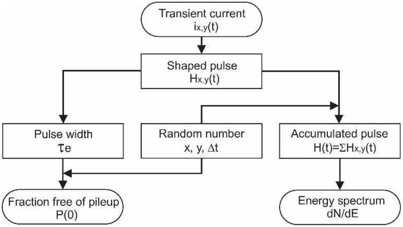
Figure 1 shows the flowchart to analyze the pulse pileup effect. First, the transient currents induced by monoenergetic photons (20 keV) interacting at different locations within the detector are calculated. Second, by passing these currents through a pulse shaping circuit (CR-RC2), the interaction-location dependent pulse shapes are calculated, and the widths of pulses are obtained by defining a threshold. Third, by taking into account the randomness (both locations and arrival times) of the successive photons interacting within the detector, and comparing the pulse width of the first photon with the time intervals between the first photon and the successive photons, the fractions of different orders of pileup are calculated. Finaly, by adding the shaped pulses according to their arrival times and interaction locations, a pulse height histogram is obtained which is then converted to an energy spectrum. The detailed software and methods used for the calculations are explained in the subsections below.
Fig. 1.
Flowchart of pulse pileup analysis process.
B. Transient Current
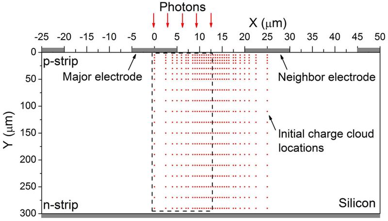
Figure 2 shows the cross-section of the DC-coupled DSSSD and the locations at which the initial charge clouds are placed for transient current calculations. The oxide layer (SiO2) between p-strips with charge area density of 1×10¹¹ q/cm2 is not shown, however it is included in the model. The n-side is biased at +50 V, which is 10 V above the full depletion value. In this study, the transient currents induced by 20 keV photons are calculated as following: First, the energy distribution of the initial charge is calculated using PENELOPE [19]. PENELOPE is a Monte Carlo code that can calculate energy depostion along a photoelectron trajectory. Ten thousand photons were simulated to obtain an averaged charge cloud. Although each photoelectron trajectory is different, after hundreds of picoseconds the difference will be averaged out due to both electrostatic repulsion and diffusion. For a 300 μm Si detector biased at 50 V, it takes more than 10 nanoseconds for both the electron and hole charge clouds to drift from the central region to the corresponding electrodes, and thus the average charge cloud can provide accurate charge sharing and pulse pileup results. For the interactions that occur near the surface of the detector, the charges will be collected before diffusing into a large size cloud. In which cases, if the interaction happens right under one electrode, then most of the charges will be collected on this electrodes; if the interaction happens in the middle region between the two adjacent electrodes, then the induced signals will be initial charge cloud dependent. However, this region should be small by comparing the size of the initial charge cloud (~ 3 μm for 20 KeV x-ray) and the pitch of the detector (25 μm). In addition, we are studying the average effect of the pulse pileup behavior of the detector, thus detailed calculation of the spatial charge distribution is unnecessary. For the above reasons, we used the averaged charge cloud to simulate the transient current and pulse shapes for pulse pileup analysis. Second, the transient currents were simulated using a 3D TCAD software ATLAS from Silvaco Inc. [20]. ATLAS is a finite element software that can calculate transient current collected on an arbitray electrode by solving Poisson and drift/diffusion equations. The interaction locations (also shown as red dots in Fig. 2) are chosen so that the energy registered by the major electrode differs by less than 1 keV between two adjacent locations (both in lateral and depth directions), where 1 keV is the energy bin used in the energy histogram (see Sec.III.D). To meet this requirement, a total number of 589 locations are chosen, but only half of these locations (within the black dashed rectangular shape in Fig.2) are simulated by exploiting geometric symmetry. For instance, the transient current collected on the neighboring electrode when placing the initial charge at x = 5 μm is equal to the transient current collected on the major electrode when placing the charge at x = 20 μm with the same depth.
Fig. 2.
Schematic cross section of the DSSSD for TCAD transient current simulation. The simulated device is 300 μm thick with a pitch of 25 μm. The silicon substrate has n-type doping of 5.6×1011 cm−3. The transient currents collected on both the major and neighbor electrodes are calculated. The major collecting electrode is the electrode with a shorter distance from the initial charge cloud compared to the neighboring collecting electrode. Detailed simulation setup can be found from [18].
In this paper, we only investigated the pulse pileup effect on the p-side of the detector. The pileup on the n-side was not studied due to a software converge issue when adding the oxide charge (an oxide charge must be included in the model for accurate transient current calculation), but we believe the n-side behaves quite similarly to the p-side under the studied geometry (300 μm) and bias condition (50V) because: 1) the dimension of the diffusing electron and hole charge clouds are the same after drifting the same distance [21]; 2) The electric field in DSSSD decreases linearly from p-side to n-side. Lower mobility holes drift toward the p-side with higher electric field, while higher mobility electrons drift toward n-side with lower electric field, and the overall effect is that the two carriers drift with a comparable speed thus arrive at the corresponding electrodes simultaneously [18]; The above two reasons result in similar charge sharing and pulse pileup behavior for both carriers, and thus study of the p-side of the detector can provide referenceable pulse pileup information for the whole structure.
C. Pulse Shaping
After calculating the transient currents for all of the locations, each current is shaped by a simple CR-RC2 pulse shaping circuit using Simulink in MATLAB [22]. The effective linear transfer function of this process is [23]
| (1) |
which incorporates the effect of one charge sensitive amplifier, one differentiator and two integrators, all with time constant τ0. A larger time constant guarantees better energy resolution due to the reduction of ballistic deficit and suppression of electronic noise, but it also results in a high rate of pileup due to the longer duration of the shaped pulses [24]. Thus, an optimal time constant should be found before further analysis (see Sec.III.B).
D. Pulse Pileup
A simple method for pulse pileup analysis which does not consider the pulse shape difference uses the concept of effective pulse width (τe) [25]. To avoid pileup, the time interval between two successive pulses must be greater than τe. The probability of observing a time interval greater than τe, i.e., the fraction free of pileup is [25]
| (2) |
and the fraction of different orders of pileup for a paralyzable system is [25]
| (3) |
where, r is the average interaction rate within the detector, and x is the order of pileup. To find τe, first, the pulse widths of all the simulated pulses shaped by an optimal time constant are calculated; the interaction rate variation along the depth direction within the detector are taken into account. Second, by examining the pulse width histogram, the averaged pulse width is defined to be the effective pulse width (Sec.III.B).
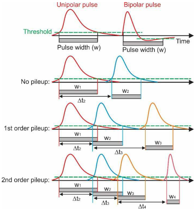
In our study, the pulse width (duration of pulse over predefined threshold) of each individual pulse depends on the location of interaction and on the collected photon energy. Both locations of interaction and arrival times are random processes described by probability density functions (Sec.II.E). Figure 3 provides a graphical description of the pileup effect. If the time interval between the first pulse and second pulse is longer than the width of the first pulse (Δt2 > w1), there is no pileup; otherwise, a pileup event occurs. The order of pileup depends on how many consecutive pulses have an arrival time interval from the previous pulse that is shorter than the width of the previous pulse. Based on this process, we can calculate the probabilistic fraction free of pileup and the different orders of pileup.
Fig. 3.
Different orders of pulse pileup. The pulse width is obtained from the shaped pulse by choosing a threshold. Pileup occurs when the time interval (Δt) between pulses of the first and the following photon is shorter than the pulse width (w1) of the first photon. Note that the pulse width of the bipolar pulse should take into account the undershoot part.
The detection threshold is determined by the electronic noise level. For our strip detector with an electrode length of 1 cm, we assume the standard deviation of the Gaussian noise distribution to be σ = 135 e- [26, 27]. By setting the detection threshold to be 2σ = 270 e-, more than 97% of the noise signal will be rejected. To generate 270 e-h pairs in silicon, a total energy of about 1 keV is required, corresponding to 0.06 arbitrary units (a.u.) for the shaped pulse (see Sec.III.A).
To calculate different orders of pileup under various photon fluxes, first, the pileups under different photon interaction rates are calculated (effective pulse width model and varied pulse shape model described above) for one electrode. Then, the flux is calculated using the relation
| (4) |
where, r again is the photon interaction rate within the detector,∅ is the photon flux in the unit of Mcps/mm2, and A is the detection area corresponding to one electrode: A = W·L. The width W is 50 μm since an electrode can detect photons interacting on both left and right sides of the electrode (see Fig.2). L is the length of the electrode, a 1 cm electrode is used in our discussion. Finally, a factor of 26.8% is used to take into account the 20 keV photon absorption coefficient and thickness of the detector (300 μm).
E. Energy Spectrum
Both interacting location and time of arrival of a photon in detector material are random processes. The probability density functions (PDF) for the lateral and depth location of each interaction and for the time interval between consecutive interactions can be expressed as
| (5) |
| (6) |
| (7) |
where P and d are the pitch and thickness of the detector, respectively. Parameter μsi is the linear attenuation coefficient of the 20 keV photon in silicon (10.4×10⁻⁴μm−1), n is the average rate of photons incident on the detector in units of Mcps, and t is time in units of seconds. Note that this rate n is different from the interaction rate r in (3), where r is the number of photon interactions per unit time within the detector, and only 26.8 % of the incident photons interact with the 300 μm detector. Based on these PDFs and the detector geometry, a series of random numbers representing the interaction locations [x, y] and the time intervals (Δt) between two successive photons can be calculated for a given photon flux.
To obtain the energy spectrum, first, a pair of random numbers [x, y] based on (5) and (6) are calculated and rounded to the locations used in the simulation, then a pulse shape is chosen according to the random numbers. Second, a random time interval Δt is calculated based on (7). Third, this pulse is added to the pulse train to generate an accumulated pulse. Fourth, the three previous steps are repeated to generate a final accumulated shaped pulse. By simulating a sufficiently large number of pulses, enough statistics can be reached to obtain a good representation of the pulse height distribution. Finally, the pulse height values are converted to energies based on their relation so that an energy histogram is obtained.
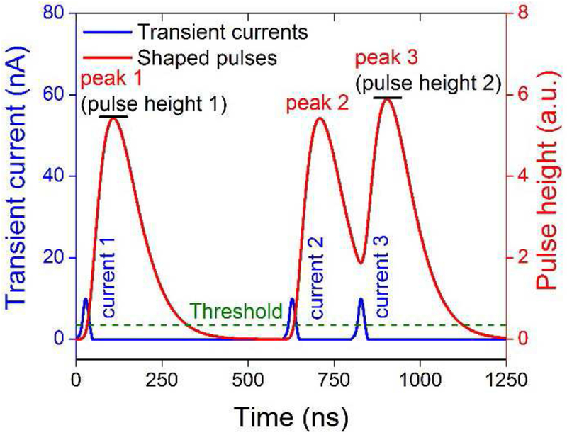
Figure 4 shows an example of the accumulated shaped pulse and the corresponding transient currents. Each pulse peak corresponds to a transient current. Since both peaks 2 and 3 are above the detection threshold, only the higher peak 3 is registered as a signal.
Fig. 4.
Accumulated shaped pulse and the corresponding transient currents. Three transient currents are shown in blue, and the corresponding three shaped pulses are in red with 3 peaks (1, 2, and 3). A threshold is set above which the highest peak value is registered as the pulse height.
The difference between the energy spectrum free of pileup and the ones with different degrees of pileup is compared quantitatively by the root mean square difference (RMSD) [4]:
| (8) |
where Ni and Ni,0 are the fractions of the number of detected events in the ith energy bin for the spectra, normalized to the total number of interaction photons, with and without pileup, respectively. Parameter N is the number of energy bins, and N = 40 in our case with 1 keV increment. The histogram covers energies between 0 and 40 keV, and energies higher than the photon energy (20 keV) are necessary in order to include the piled up energies.
III. Results and Discussion
A. Transient Current and Shaped Pulse
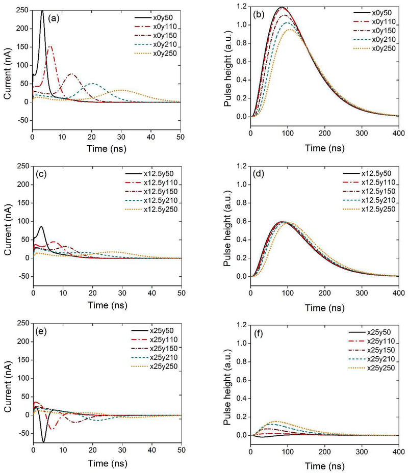
Figures 5 (a–f) show the transient currents and the corresponding shaped pulses for the major collecting electrode when placing the initial charge at the various locations illustrated in Fig.2. For charge clouds initiated at x = 0 μm, i.e., right under the major electrode, as the depth (i.e. y) increases, first, the time for the transient current to form peaks becomes longer (Fig.5(a)), so that the collecting time or peaking time (the time for the signal to rise from baseline to its peak value) shown in Fig.5(b) becomes longer. second, the area under the transient current becomes smaller, indicating that fewer charges are collected on the major electrode (the rest is collected on the neighbor electrode), and the peak of the shaped pulse becomes lower (Fig.5(b)).
Fig. 5.
Transient currents (left column) and the corresponding shaped pulses (right column) collected on the major electrode when placing the initial charge cloud at different locations: as an example, x12.5y50 indicates the charge cloud initiated at (x, y) = (12.5, 50) μm. The arbitrary units are scaled so that 1.2 a.u. corresponds to 20 keV.
When the initial charge is placed at x=12.5 μm, in the middle between the major and neighbor electrode, the amplitudes of the shaped pulses (Fig.5(d)) collected on the major electrodes are almost the same, because the same number of charges, i.e., half of the total liberated charges are collected on the major electrode. The peaking time increases with depth of interaction. However, the increase from y=50 μm to y=150 μm is less than that from y = 150 μm to y = 250 μm. This is because in a p-n junction, the electric field in the top p-side is higher than the bottom n-side, and holes (p-side mainly collecting holes) move faster on the top p-side resulting in a shorter charge collection time
When placing the initial charge right under the neighbor electrode, i.e. at x=25 μm, some of the transient currents collected on the major electrode show a bipolar behavior (Fig.5(e)), which results in bipolar shaped pulses (Fig.5(f)). This is because the weighting field changes polarity near the neighboring electrode [28]. In addition, due to the small amount of charge collected on the major electrode, some pulses may have amplitudes lower than the detection threshold and thus, cannot be registered as signals.
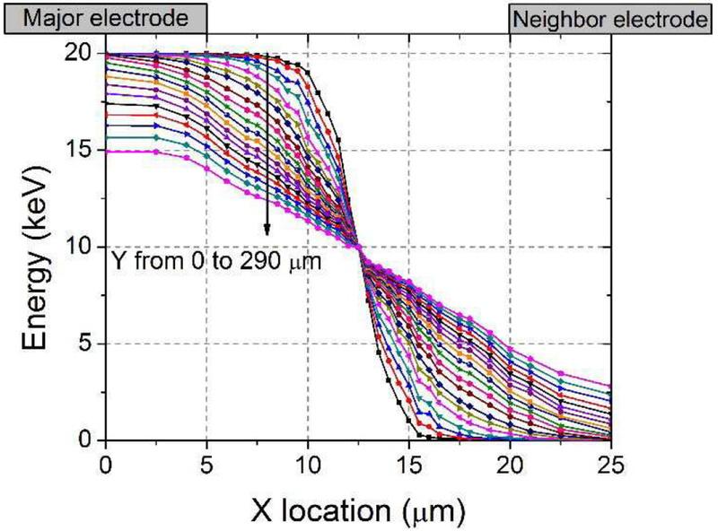
Figure 6 shows the energy collected on the major electrode when placing the initial charge at various locations. The energy is obtained as follows: first the transient current is integrated to obtain charge, then the energy is calculated by taking into account the ionization energy (3.62 eV per e-h pair) and the charge of a single electron (1.602×10⁻¹⁹ C). When the initial charge cloud is placed between x=0 and 7.5 μm, most of the charges (or energy) are collected on the major electrode. When the cloud is placed between x=17.5 and 25 μm, only a few charges are collected on the major electrode. The lateral locations in between have a large effect on the charge sharing between the two electrodes. This result is consistent with the previous discovery that a silicon-strip detector can be divided into three regions, with different charge sharing behavior [29]. A large number (589) of locations are calculated so that > 90 % of the difference of the collected energies between the two adjacent locations (both in lateral and depth directions) is < 1 keV, to guarantee an accurate energy spectrum with a 1 keV energy bin.
Fig. 6.
Energy collected on the major electrode when placing the initial charge cloud at different locations. The collected charge is sensitive to lateral locations when the cloud is placed in the middle region that extends from 7.5 to 17.5 μm.
B. Effective Pulse Width
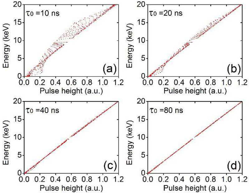
Figure 7 shows the energy deposited vs. pulse height when placing the initial charge at various locations within the detector for different pulse shaping time constants (τ0 in (1)). There is a tradeoff between energy resolution and extent of pileup when choosing a pulse shaping time constant. As τ0 increases, a better linear relation can be observed between the energy deposited and pulse height since the ballistic deficit decreases. However, when τ0is higher, there is also more pileup because of increased probability of pulse overlap due to longer pulse width. Since high energy resolution is required to guarantee a high spatial resolution for strip detectors,we chose a time constant that keeps the energy distortions < 1 keV. Based on this standard, 40 ns is chosen (Fig.7(c)) and a linear relation with a high R-squared value is found:
| (9) |
where E is the energy in units of keV, and H is the pulse height in arbitrary units.
Fig. 7.
Energy deposited vs. pulse height under different time constants. The pulse height is obtained by passing the transient current through a CR-RC2 shaping circuit. The energy is obtained by integrating the transient current.
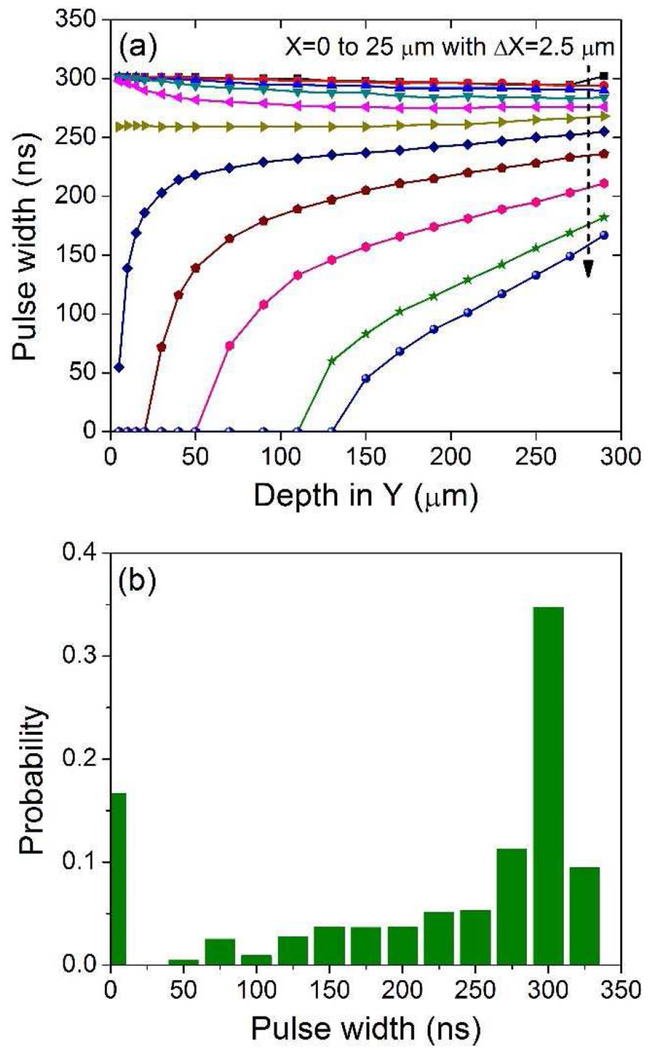
Using the 40 ns time constant and a detection threshold of 0.06 a.u. (corresponding to 1 keV), Fig. 8 (a) plots the pulse widths of the shaped pulses when placing the initial charge at some representive locations. The pulse widths are widely spread between 0 and 325 ns. Fig.8 (b) plots the histogram of the pulse widths by taking into account the photon interaction rate within the detector, i.e., the exponential decay of rate of interaction as a function of depth in the detector. The mode is 300 ns. However, since a large number of pulses have widths less than 300 ns, we defined the effective pulse width to be the average pulse width, i.e., 215 ns, weighted by the number of occurrences of various pulse widths. A zero pulse width indicates that the pulse height is lower than the detection threshold and thus, cannot be registered as a signal. Calculations indicate that ~16% of the photon signals is lost. According to Fig. 8 (a), these are events occurring close to the neighboring electrode at shallow depth.
Fig. 8.
(a) Pulse widths of the shaped pulses when the charge cloud is initiated at different locations. (b) Pulse width histogram by taking into account the interaction probability along the depth in the detector.
C. Pileup Analysis
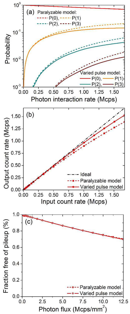
At bias voltage of 50 V, Fig. 9 (a) plots the probability for different orders of pileup calculated from the varied pulse shape model and the paralyzable detector model with effective pulse width of 215 ns based on (3). Figure 9 (b) compares the output count rate under different input count rates, i.e., photon interaction rates within the detector. The two models provide similar results, proving that the definition of effective pulse width is reasonable.
Fig. 9.
(a) The probability of different orders of pulse pileup for paralyzable and varied pulse shape models. P(0) is the fraction free of pileup, P(1), P(2) and P(3) are the first, second, and third orders of pileup, respectively. (b) Count rate performance for paralyzable and varied pulse shape models. (c) Fraction free of pileup under different photon fluxes. To obtain good statistics, 1 million incident photons are simulated. The simulated detector has a thickness of 300 μm, pitch of 25 μm, strip length of 1 cm, and bias voltage of 50 V.
For a 25 μm pitch detector with strip length of 1 cm biased at 50 V, the fractions free of pileup under different photon fluxes is calculated from (4) as shown in Fig.9 (c). To keep the fraction > 90%, both models predict a photon flux of ~ 3.75 Mcps/mm2. The photon flux is comparable to most state-of-the-art photon counting detectors employing either pixelated or strip geometry, which are in the range between several to tens of Mcps/mm2 (see Table I in [30]). Note that the pileup effect can be reduced by employing higher bias voltages. In addition, once the detector geometry (i.e., pitch, strip length and thickness) and bias voltage are chosen, pileup is solely determined by the photon incident rate onto a detector unit. Thus, the results in Fig.9 can also be used for strip detectors utilizing small-angle stereo geometry, in which the angle between the front and back strips is less than 90°. Use of a stereo geometry can reduce the amount of ghost signals for detectors operating in high photon flux environment by reducing the number of overlapped strips on the two opposite sides [31].
TABLE I.
RMSD of the energy histograms under different photon fluxes
| Photon flux (Mcps/mm2) | RMSD (×10−2) |
|---|---|
| 1.25 | 0.31 |
| 6.25 | 1.25 |
| 12.5 | 3.80 |
D. Energy Spectrum
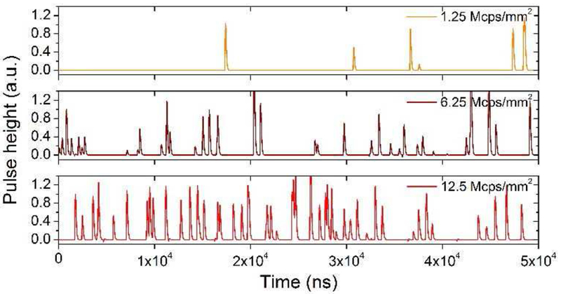
For the detector with strip length of 1 cm and biased at 50 V, the pulse height signals of accumulated successive photons are shown in Fig.10, by considering the interaction locations, times of arrival and the photon incident flux. Three fluxes of 1.25, 6.25, and 12.5 Mcps/mm2 are compared. The pileup becomes significant as the incident flux increases.
Fig. 10.
Accumulated pulse height signal under different photon incident fluxes. High flux results in high ratio of pileup. The simulated detector is 300 μm thick with pitch of 25 μm.
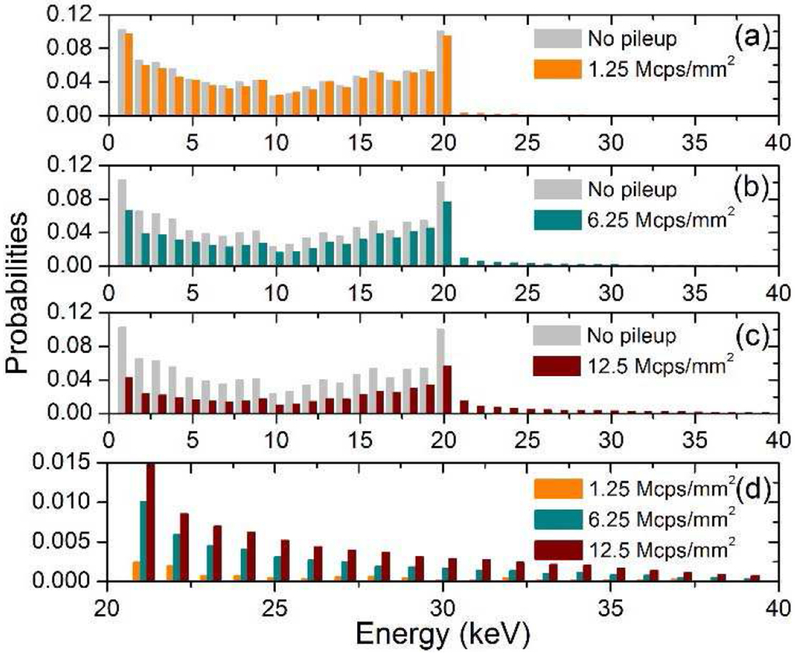
From the accumulated pulse height signal, an energy histogram can be created from (9). Figures 11 (a), (b) and (c) compare the energy histograms in a single electrode under three photon fluxes against one with no pileup. The bimodal characteristic, i.e., with two peaks at the two ends of the spectrum, has been observed from both experimental and simulation results [32–34]. Figure 11 (d) compares the corresponding histograms with pileup in the 20-40 keV range. With higher incident flux, more photons pile up, thus a large number of low energy counts move toward the high energy range. In addition, due to charge sharing between the two adjacent electrodes, energies detected by one electrode vary between 0 and 20 keV, so pileup is also prevalent in the low energy range (< 20 keV).
Fig. 11.
Energy histograms under different photon incident fluxes. The energy bin is 1 keV and 40 bins are used. The simulated detector has a thickness of 300 μm, pitch of 25 μm, strip length of 1 cm, and is biased at 50 V.
The root mean square difference (RMSD) of the spectra under various photon fluxes compared to the one without pileup are listed in Table I. Basically, the RMSD becomes higher at higher photon flux. By linear interpolation, a photon flux of 3.75 Mcps/mm2 corresponds to RMSD of 0.78×10⁻². Thus, in order to guarantee > 90% photons free of pileup, the RMSD of the energy histogram should be smaller than this value.
E. Electronic Noise and Different Photon Energies
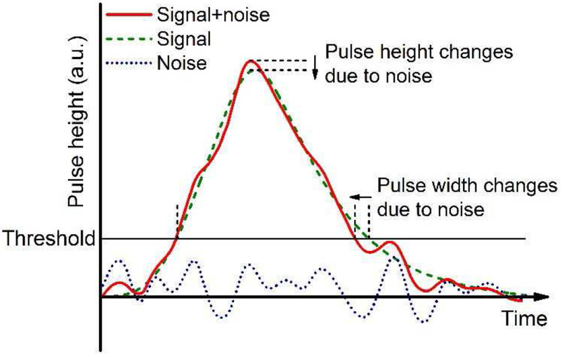
The previous discussion does not take into account electronic noise. Electronic noise results in degradation of energy resolution, inducing false trigger if the lowest energy threshold is set below the noise floor. Electronic noise adds more stochastic components to the amplitude of the pulse height (Fig. 12), leading to loss of energy resolution. Degradation of energy resolution can cause degradation in spatial resolution when using photon interaction position estimation algorithms such as the center-of-gravity method [20]. Electronic noise may also affect the detector’s count-rate capability. Due to electronic noise, the pulse width can increase or decrease since the time when the threshold is crossed changes due to the addition of the noise waveform (see Fig.12). However, we assume the net effect of the electronic noise on the count-rate capability to be minor, since the probabilities that the pulse is shortened or lengthened are approximately similar.
Fig. 12.
Waveforms of the pure signal (green dash), electronic noise (blue dot) and signal plus noise (red). Due to noise, both pulse width and pulse height are changed.
In addition, photons in CT and mammography systems have polychromatic spectra instead of the monoenergetic spectrum assumed in our calculations. Previous studies showed that signal shape is almost independent of the deposited energy for the same interaction locations [23, 35]. This allows the use of the 20 keV photon pulse shape to derive pulse pileup behavior including other energies. Using this method, the pulse pileup effect under polychromatic illumination can be calculated without additional transient current simulations. For a first order approximation, the pulse width for the lower energy photons (< 20 keV) should be smaller than the 20 keV photons use in our calculation due to the reduced charge cloud size, thus the corresponding pileup effect for the low energy photons should be smaller.
IV. Conclusions
In this paper, we analyzed the pulse pileup effect for a double-sided silicon strip detector. Pulses are dependent on transient current that in turn are dependent on interaction location within the detector and show unipolar or bipolar behavior. Different orders of pileup under different photon fluxes were calculated. For a detector with a pitch of 25 μm, strip length of 1 cm, under a bias voltage of 50 V, and a detection threshold of 1 keV, the calculated fraction free of pileup can be > 90 % under a photon flux of 3.75 Mcps/mm2 for photons with energy ≤ 20 keV (i.e., photons for mammography application). In addition, by defining the effective pulse width to be the average pulse width, pileup results from paralyzable model were in good agreement with results from the variable pulse shape model. This indicates that a reasonable averaged pulse shape or averaged pulse width can be used to estimate the pile up effect for DSSSDs. Furthermore, using the variable pulse shape model, the energy spectra under different photon fluxes were calculated, and the pileup effect was evaluated by root mean square difference (RMSD) with the spectrum without pileup. Note that for a fixed photon fluence, the pileup effect can be further reduced by employing high bias voltages, smaller pixel size/strip pitch, stacked multilayer detector, multi-well solid state detector (MWSD) [36], field-Shaping multi-Well Avalanche Detector(SWAD) [37], and/or an advanced shaping circuits, such as one with pileup rejection capability [23].
Several factors may be addressed to further improve the accuracy of the pileup analysis model. First, in our model, the photon interaction locations are rounded to some specific locations (in total 589 locations), and the accuracy of the pulse shape when a photon interacts at arbitrary locations is thus deteriorated. More accurate pulse shapes could be obtained by linear interpolation between the simulated interaction locations. Second, only the p-side of the device is studied, and the pulse pileup on the n-side may be slightly different. Third, pulse pileup causes energy distortion, which finally affects the spatial resolution of the reconstructed photon interaction locations. The effect of pulse pileup in conjunction with electronic noise on spatial resolution requires further study. In addition, the effect of pulse pileup on the covariance of the measured counts at different recorded energies is also a subject of future study. Despite these limitations, the study shows that photon counting DSSSD can work in moderate photon flux environments, and thus, is a promising candidate for mammography applications. In addition, the proposed method can be used to analyze other types of photon counting detectors where pulse shapes vary depending on detector operational conditions.
Acknowledgments
The author Jinghui Wang thanks Dr. Norbert Pelc and Dr. Lei Zhu for their constructive suggestions. The authors thank silvaco inc. for their software support. some of the computing for this project was performed on the Sherlock cluster. We would like to thank the Stanford Research Computing Center for providing computational resources and support that contributed to these research results.
This work is supported by the Stanford-Coulter Translational Research Grant and by NIH R21 EB020299 ‘Charge Cloud Tracker: a high-resolution, high-DQE, photon counting energy-discriminating x-ray detector’.
Footnotes
Disclosure of conflicts of interest
M.P. discloses financial interests in Prismatic Sensors AB. All other authors have no relevant conflicts of interest to disclose.
Contributor Information
Jinghui Wang, J. Wang was with the Department of Radiology, Stanford University, Stanford, CA 94305 USA. He is now with the Department of Radiation Oncology, Stanford University, Stanford, CA 94305 USA.
Linchuan Chen, L. Chen was with the Department of Computer Science and Engineering, The Ohio State University, Columbus OH 43210 USA. He is now with Google, 1600 Amphitheatre Parkway, Mountain View, CA 94043 USA.
Mats Persson, M. Persson is with the Department of Bioengineering, Stanford University, Stanford, California 94305 USA.
Paurakh L. Rajbhandary, P. L. Rajbhandary was with Department of Bioengineering, Stanford University, Stanford, CA 94305 USA
Praneeth Kandlakunta, P. Kandlakunta is with the Department of Mechanical and Aerospace Engineering, The Ohio State University, Columbus, OH 43210 USA.
Gabriella Carini, G. Carini was with the SLAC National Accelerator Laboratory, Menlo Park, CA 94025 USA. She is now with the Brookhaven National Laboratory, Upton, NY 11973 USA.
Rebecca Fahrig, R. Fahrig was with the Department of Radiology, Stanford University, Stanford, CA 94305 USA. She is now with Siemens Healthcare GmbH, Erlangen, 91052 Germany, also with Pattern Recognition Lab, Friedrich-Alexander-University, Erlangen-Nuremberg, 91052 Germany.
References
- [1].Hsieh SS, and Pelc NJ, “Improving pulse detection in multibin photon-counting detectors. Journal of Medical Imaging,” J. Med. Imag, vol. 3, no. 2, pp. 023505-1–023505-7, 2016. [DOI] [PMC free article] [PubMed] [Google Scholar]
- [2].Cammin J, Kappler S, Weidinger T, and Taguchi K, “Evaluation of models of spectral distortions in photon-counting detectors for computed tomography,” J. Med. Imag, vol. 3, no. 2, pp.023503-1–023503-12, 2016 [DOI] [PMC free article] [PubMed] [Google Scholar]
- [3].Taguchi K, “Energy-sensitive photon counting detector-based X-ray computed tomography,” Radiol. Phys. and Technol, Vol. 10, no. 1, p. 8–22, 2017. [DOI] [PubMed] [Google Scholar]
- [4].Taguchi K, Frey EC, Wang X, Iwanczyk JS, and Barber WC, “An analytical model of the effects of pulse pileup on the energy spectrum recorded by energy resolved photon counting x-ray detectors,” Med. Phys, 2010. vol. 37, no.8, pp. 3957–3969, 2010. [DOI] [PMC free article] [PubMed] [Google Scholar]
- [5].Persson M, Bujia R, Nowik P, Andersson H, Kull L, Andersson J et al. , “Upper limits of the photon fluence rate on CT detectors: Case study on a commercial scanner,” Med. Phys, vol. 43, no. 7, pp. 4398–4411, 2016. [DOI] [PubMed] [Google Scholar]
- [6].Abbene L, Gerardi G, Principato F, Sordo SD, Lenzi R, and Raso G, “High-rate x-ray spectroscopy in mammography with a CdTe detector: A digital pulse processing approach,” Med. Phys, 2010. vol. 37, no. 12, p. 6147–6156, 2010. [DOI] [PubMed] [Google Scholar]
- [7].Boone JM, Fewell TR, and Jennings RJ, “Molybdenum, rhodium, and tungsten anode spectral models using interpolating polynomials with application to mammography,” Med. Phys, vol. 24, no. 12, pp. 1863–1874, 1997. [DOI] [PubMed] [Google Scholar]
- [8].Saito M, “Dual-energy approach to contrast-enhanced mammography using the balanced filter method: Spectral optimization and preliminary phantom measurement,” Med. Phys, vol.34, no.11, pp. 4236–4246, 2007. [DOI] [PubMed] [Google Scholar]
- [9].Chen H, Cederström B, Xu C, Persson M, Karlsson S, Danielsson M, “A photon-counting silicon-strip detector for digital mammography with an ultrafast 0.18-μm CMOS ASIC,” Nucl. Instrum. Methods Phys. Res. A, Accel. Spectrom. Detect. Assoc. Equip,vol. 749, pp. 1–6, 2014. [Google Scholar]
- [10].Wielopolski L, Gardner RP, “Prediction of the pulse-height spectral distribution caused by the peak pile-up effect,” Nucl. Instrum. Methods Phys, vol.133, no. 2, pp. 303–309, 1976. [Google Scholar]
- [11].Wielopolski L, Gardner RP, “A generalized method for correcting pulse-height specra for The peak pile-up effect due to double sum pulses,” Nucl. Instrum. Methods Phys, vol. 140, no. 2, pp. 289–296, . [Google Scholar]
- [12].Frey EC, Wang X, Du Y, K Taguchi, J Xu, and Tsui BMW, “Investigation of the use of photon counting x-ray detectors with energy discrimination capability for material decomposition in micro-computed tomography,” Proc. of SPIE, San Diego, CA, USA, Mar. 2007, pp. 65100A-1–65100A-11. [Google Scholar]
- [13].Taguchi K, Zhang M, Fery EC, Wang X, Iwanczyk JS, Nygard E et al. , “Modeling the performance of a photon counting x-ray detector for CT: Energy response and pulse pileup effects,” Med. Phys, vol. 38, no. 2, pp. 1089–1102, 2011. [DOI] [PMC free article] [PubMed] [Google Scholar]
- [14].Cammin J, Xu J, Barber WC, Iwanczyk JS, Hartsough NE, and Taguchi K, “A cascaded model of spectral distortions due to spectral response effects and pulse pileup effects in a photon-counting x-ray detector for CT,” Med. Phys, vol. 41, no. 4, pp. 041905-1–041905-15, 2014. [DOI] [PMC free article] [PubMed] [Google Scholar]
- [15].Oishi T, and Baba M, “Development of Pile-up Separation Method Using Digital Signal Processing,” J. Nucl. Sci. Technol, vol.45, pp. 375–378, 2008. [Google Scholar]
- [16].Chaplin V, Bhat N, Briggs MS, Connaughton V, “Analytical modeling of pulse-pileup distortion using the true pulse shape; applications to Fermi-GBM,” Nucl. Instrum. Methods Phys. Res. A, Accel. Spectrom. Detect. Assoc. Equip, vol.717, pp. 21–36, 2013. [Google Scholar]
- [17].Cano-Ott D, Tain JL, Gadea A, Rubio B, Batist L, Karny M et al. , “Pulse pileup correction of large NaI(Tl) total absorption spectra using the true pulse shape,” Nucl. Instrum. Methods Phys. Res. A, Accel. Spectrom. Detect. Assoc. Equip, vol. 430, no.2-3, pp. 488–497, 1999. [Google Scholar]
- [18].Wang J, Carini G, and Fahrig R, “Using depth of interaction and charge sharing effect to achieve ultrahigh spatial resolution on double sided silicon strip detectors,” in review IEEE Trans. Nucl. Sci. [DOI] [PMC free article] [PubMed] [Google Scholar]
- [19].Salvat F, Fernández-Varea JM and Sempau J, “PENELOPE-2011: A Code System for Monte Carlo Simulation of Electron and Photon Transport,” NEA/NSC/DOC(2011)/5, OECD Nuclear Energy Agency, Issy-les-Moulineaux, 2011. [Google Scholar]
- [20]. www.silvaco.com/.
- [21].Talla PT, “Investigation of photon counting pixel detectors for X-rayspectroscopy and imaging,” Ph.D. dissertation, Erlangen Centre of Astroparticle Physics, Friedrich-Alexander-University Erlangen-Nürnberg, Erlangen, Germany, 2011 [Google Scholar]
- [22]. https://www.mathworks.com/products/simulink.html.
- [23].Bornefalk H, Xu C, Svensson C, and Danielsson M, “Design considerations to overcome cross talk in a photon counting silicon strip detector for computed tomography,” Nucl. Instrum. Methods Phys. Res. A, Accel. Spectrom. Detect. Assoc. Equip, vol. 621, no. 1-3, pp. 371–378, 2010. [Google Scholar]
- [24].Guo W, Lee SH. Gardner RP, “The Monte Carlo approach MCPUT for correcting pile-up distorted pulse-height spectra,” Nucl. Instrum. Methods Phys. Res. A, Accel. Spectrom. Detect. Assoc. Equip, vol. 531, no. 3, pp. 520–529, 2004. [Google Scholar]
- [25].Knoll GF, Radiation Detection and Measurement. 3rd ed Hoboken, NJ, USA: John Wiley & Sons, Inc., 1999, pp. 119–122. [Google Scholar]
- [26].Grybos P, Kachel M, Kmon P, Szczygiel R, Tagucho T, “Low Noise 64-Channel ASIC for AC and DC Coupled Strip Detectors,” IEEE Trans. Nucl. Sci, vol. 58, no.1, pp. 187–193, 2011. [Google Scholar]
- [27].Tajima H, Kamae T, Uno S, Nakamoto T, Fukazawa Y, Mitani T, et al. , “Low noise double-sided silicon strip detector for multiplecompton gamma-ray telescope,” Proc. SPIE 4851, X-Ray and Gamma-Ray Telescopes and Instruments for Astronomy, vol.4851, pp.875–884, 2003. [Google Scholar]
- [28].Spieler H, Semiconductor Detector Systems. NY, USA: Oxford University Press Inc., 2008, pp.71–82. [Google Scholar]
- [29].Turchetta R, “Spatial resolution of silicon microstrip detectors,” Nucl. Instrum. Methods Phys. Res. A, Accel. Spectrom. Detect. Assoc. Equip,vol. 335, no. 1-2, pp. 44–58, 1993. [Google Scholar]
- [30].Taguchi K, and Iwanczyk JS, “Vision 20/20: Single photon counting x-ray detectors in medical imaging,” Med. Phys, vol. 40, no. 10, pp. 100901-1–100901-19, 2013. [DOI] [PMC free article] [PubMed] [Google Scholar]
- [31].Powell W, “Development of a Silicon Tracker and Front-End Electronics for R3B,” Ph.D. dissertation, University of Liverpool, Liverpool, UK, 2016. [Google Scholar]
- [32].Belau E, Klanner R, Lutz G, Neugebauer E, Seebrunner HJ, Wylie A et al. , “Charge collection in silicon strip detectors,” Nucl. Instrum. Methods Phys. Res, vol. 214, no. 2-3, pp. 253–260, 1983. [Google Scholar]
- [33].Passeri D, Ciampolini P, Baroncini M, Santocchia A, Bilei GM, Checcucci B et al. , “Comprehensive modeling of silicon microstrip detectors,” IEEE Trans. Nucl. Sci, vol. 44, no.3, pp. 598–605, 1997. [Google Scholar]
- [34].Straulino S, Adriani O, Bonechi L, Bongi M, Bottai S, Castellini G et al. , “Spatial resolution of double-sided silicon microstrip detectors for the PAMELA apparatus,” Nucl. Instrum. Methods Phys. Res. A, Accel. Spectrom. Detect. Assoc. Equip, vol. 556, no.1, pp. 100–114, 2006. [Google Scholar]
- [35].Cederstrom B, Danielsson M, Lundqvist M, and Nygen D, “High-resolution X-ray imaging using the signal time dependence on a double-sided silicon detector,” Nucl. Instrum. Methods Phys. Res. A, Accel. Spectrom. Detect. Assoc. Equip, vol. 423, no. 1, pp. 135–145, 1999. [Google Scholar]
- [36].Golan AH, Rowlands JA, Tousignant O, and Karim KS, “Unipolar time-differential charge sensing in non-dispersive amorphous solids,” J. Appl. Phys, vol. 113, no.22, pp. 224502-1–224502-12, 2013. [Google Scholar]
- [37].Stavro J, Goldan AH, and Zhao W, “Photon counting performance of amorphous Selenium and its dependence on detector structure,” Proc. SPIE, Medical Imaging 2018: Physics of Medical Imaging, vol.10573, pp. 105735Y-1–105735Y-10, 2018. [DOI] [PMC free article] [PubMed] [Google Scholar]


